

Abstract
Ambient pressure X-ray photoelectron spectroscopy (APXPS) is combined with simultaneous electrical measurements and supported by density functional theory calculations to investigate the sensing mechanism of tungsten disulfide (WS2)-based gas sensors in an operando dynamic experiment. This approach allows for the direct correlation between changes in the surface potential and the resistivity of the WS2 sensing active layer under realistic operating conditions. Focusing on the toxic gases NO2 and NH3, we concurrently demonstrate the distinct chemical interactions between oxidizing or reducing agents and the WS2 active layer and their effect on the sensor response. The experimental setup mimics standard electrical measurements on chemiresistors, exposing the sample to dry air and introducing the target gas analyte at different concentrations. This methodology applied to NH3 concentrations of 100, 230, and 760 and 14 ppm of NO2 establishes a benchmark for future APXPS studies on sensing devices, providing fast acquisition times and a 1:1 correlation between electrical response and spectroscopy data in operando conditions. Our findings contribute to a deeper understanding of the sensing mechanism in 2D transition metal dichalcogenides, paving the way for optimizing chemiresistor sensors for various industrial applications and wireless platforms with low energy consumption.
Keywords: operando spectroscopy, band bending, surface potential, density functional theory, gas sensing
Among the various transducing schemes for gas sensor devices,1,2 chemiresistivity is the most prevalent owing to its ease of fabrication and operation. A chemiresistive device relies on measuring the change in the electrical resistance of a gas-sensing material induced by the interaction with gas molecules. These sensors are typically based on semiconductor metal oxides (ZnO, SnO2, etc.)3 or on novel 2D transition metal dichalcogenides (TMDs),4 with the latest one recently emerging to answer the demand for developing highly sensitive, selective, and low power-consuming sensors, since they can operate at a lower temperature (i.e., low energy consumption), which is critical for various industrial applications and wireless platforms. TMDs comprise a transition metal and a chalcogen, with tungsten disulfide (WS2) and molybdenum disulfide (MoS2) being the most studied.
In conventional gas sensors based on metal oxides, the interaction between surface-adsorbed oxygen-negative ions and gas molecules dominates the sensing mechanism, affecting material conductivity.5,6 They are typically operated at high temperatures, above a few hundred degrees Celsius, to accelerate the reduction/oxidation reactions and reduce water adsorption on the sensing material surface, mainly when operating in a humid environment. However, room-temperature (RT) operation has also been achieved for nanostructured oxides.7
In the case of layered materials, it has been reported that the sensing mechanism is mainly based on the charge transfer processes between the sensing material, which acts as a charge acceptor or donor, and the gas molecules. The nature of the interaction can vary, but often, the best performances are obtained when the charge transfer mechanism is based on the physisorption of the gas molecules without any molecule fragmentation, which would require a high temperature for the reactivation of the sensing surface.8,9
WS2 has a layered structure with a smaller bandgap and superior conductivity compared to metal oxides. These properties enable lower operation temperatures and render them suitable for portable, low-energy consumption applications. Additionally, the high surface-to-volume ratio in 2D TMDs offers significant potential for detecting large amounts of target analytes per unit area with rapid response and recovery times, as in the case of vertically aligned WS2 nanosheets.10 For these reasons, they have become a focal point of extensive research efforts in the past decade.7,11−13
These sensors have demonstrated high performance in detecting low concentrations of target gases (ppm range), such as H2, NH3, and NO2, with excellent thermal stability when operated at 150–160 °C.14,15 Notably, ultrasensitive detection of 800 ppb of NO2 has been reported, even at RT.16 Improved performance of WS2-based sensors is also achieved through surface functionalization to form heterojunctions with WO3,17 CuO,18 or gold decoration.19 Recent demonstrations of scalable synthesis of 2D TMDs have shown promise for the fabrication of cost-effective sensors that can be miniaturized and integrated into wearable electronic devices.20
Electrical conductivity measurements alone cannot answer many questions about the sensing mechanism. Therefore, many other experimental and theoretical techniques are commonly employed, such as photoluminescence,21 Kelvin probe force microscopy,22,23 Raman,24 ultraviolet photoemission spectroscopy,23 X-ray spectromicroscopy,25 X-ray absorption spectroscopy,26−28 and density functional theory (DFT).8,29,30 The change in the band structure induced by the interaction between the target gas analyte and the semiconductor sensing material surface is reflected in band bending: the electrostatic interaction occurring during the physisorption of the gas molecules on the surface leads to a redistribution of the electron density, which alters the surface potential, consequently changing the semiconductor conductivity and enabling the detection and measurement of various gases. If chemisorption occurs, then gas molecules undergo surface reactions with specific catalytic sites on the sensor surface, inducing modifications in the sensor properties. These catalytic surface reactions play a pivotal role in enabling the selective identification of target gases.
Nevertheless, an experiment directly examining the interaction between the gas at partial pressures relevant to atmospheric conditions and the sensing material is necessary to address the open questions related to sensor optimization. X-ray photoelectron spectroscopy (XPS) is a highly effective surface science technique that enables the investigation of modifications in the chemical environment of a sample surface and its electronic states owing to its exceptional surface sensitivity. The requirement for ultrahigh-vacuum (UHV) conditions previously limited the use of XPS in reactive environments. However, the development of ambient pressure (AP) XPS instruments has overcome this limitation, allowing for in situ and operando investigation of solid–gas interfaces under more realistic conditions, with pressures in the millibar range, such as conditions mimicking the real environment of an operating device, i.e., ppm concentration of toxic gas in air, different relative humidity, variable temperature, etc.31,32
There are recent reports of ambient pressure X-ray photoelectron spectroscopy (APXPS) being used to study the sensing mechanism of metal oxide-based sensing devices,6,33−38 while very few have used it to investigate TMDs.25,39 However, most of these previous studies have encountered challenges in concurrently measuring the electrical response and electronic properties, thus limiting the potential of operando dynamic APXPS to in situ static measurements. We summarize the most significant reports in the following paragraphs.
Jensen and coauthors studied the interaction between NOx and a MoS2 transistor by near-AP scanning photoelectron microscopy at a pressure of 8 × 10⁻⁴ mbar.25 They reported on the effect of charge transfer on the doping level of MoS2 when exposed to NOx compared with UHV conditions. This is, however, still far from a realistic working condition for a sensing device since UHV was needed to observe the effect.
In another work, Minekazi et al.39 used APXPS and DFT to investigate the hydrogen sensing mechanism of chemiresistive WS2 gas sensors on a silicon substrate. APXPS measurements were performed stepwise, exposing the sample to 1000 and 5000 ppm of H2, starting from UHV, at RT and 150 °C. Small changes in the core-level component ratios and lineshapes were observed when hydrogen was introduced, suggesting the physisorption of H2 on WS2 at RT.
Kucharski et al.33 reported on the simultaneous APXPS (albeit in discrete points) and resistance measurements on a sensing device based on a metal oxide sample. They investigated the role of surface oxygen vacancies in SnO2 to detect O2. Combining these techniques, they could correlate the surface vacancy density, sensor resistance, and band bending. Therefore, they could show that the resistance response in tin oxide gas sensors is correlated to surface oxygen vacancies. They concluded that surface oxygen vacancies, not oxygen adsorbates, cause the response observed, thus challenging the current conviction about sensing mechanisms.1,6,40 Their work highlights the great potential of APXPS in understanding the physicochemical mechanisms of gas sensing devices.
In the study presented in this article, we use APXPS and simultaneous electrical measurements to establish a direct correlation between the change in surface potential and the resistivity of the WS2 sensing material during gas-active layer interaction. To demonstrate the difference between the interaction with an oxidizing and a reducing toxic gas agent, we investigated NH3 (100, 230, and 760 ppm) and NO2 (14 ppm). The experimental findings are further supported by theoretical calculations that reproduce and justify our observations.
Our measurement procedure fully reflects the protocol of standard electrical measurements on chemiresistors: the sample is exposed to dry air, then a pulse of the target gas analyte diluted in dry air at different concentrations is introduced in the chamber for 5 min while keeping the same total pressure, and then the system is purged again in dry air without passing through unrealistic vacuum conditions.
Our selection of WS2 as a sensing material was not based on the performances shown in our measurements. Instead, it was driven by the comparatively limited comprehension of the sensing mechanism in TMDs compared to extensively researched metal oxide-based devices and their significant potential for future low-power consumption devices. The choice of the target gases is based on our previous work, where we observed promising responses from WS2-based gas sensors toward NH3 and NO2, whereas they were insensitive to CO and H2.41
The quality of the reported measurements with fast acquisition time and a 1:1 correlation between electrical response and spectroscopy data under operando conditions is a benchmark for future use of APXPS to study sensing devices.
Materials and Methods
WS2 Growth
Tungsten disulfide nanomaterials were obtained from the combination of aerosol-assisted chemical vapor deposition (AACVD) and atmospheric pressure CVD (APCVD). In the first step, tungsten trioxide nanoneedles were directly grown onto alumina sensor transducers from the AACVD of 50 mg of tungsten hexacarbonyl (W(CO)6) dissolved in a mixture of acetone and methanol. The substrate consists of an alumina piece of 4 mm × 25 mm with integrated Pt interdigitated electrodes. Before the reaction was started, the substrates were cleaned with acetone and ethanol, dried with air, and placed inside the stainless-steal reactor, which was heated at 400 °C during the synthesis. Next, the mixture of the precursor and solvents was converted to aerosols via an ultrasonic bath, which was transported to the reactor via nitrogen as a carrier gas. The flow was maintained at 0.5 L/min during the deposition for 45 min. Afterward, the obtained WO3 nanoneedles were annealed to 500 °C for 2 h under dry air to clean the substrate from the solvent residues and crystallize the nanoneedles.
In the second step, the annealed films were subjected to a sulfurization process at atmospheric pressure using a quartz tube-in-tube reactor. Two alumina boats were filled with 800 mg of sulfur (400 mg each). The first one was placed alongside the WO3 nanoneedle substrate inside the small tube, at the position where the temperature reaches 900 °C, and the second one was placed in the entrance of the big quartz tube, where the temperature is at 40 °C (Figure 1a). We used this configuration to ensure a sulfur supply during the entire reaction. Before starting the process, the APCVD reactor was flushed with 100 mL/min of argon for 1 h to remove oxygen species. Afterward, the argon flow was reduced to 30 mL/min during the whole process. The heaters were turned on, and after 30 min, the large quartz tube was pushed 10 cm toward the hot area to move the second sulfur boat from the temperature of 40 to 400 °C (Figure 1b) to supply more sulfur vapor and have a complete sulfurization of the WO3 nanoneedles. At the end of the reaction, the heaters were turned off, and the quartz tubes were naturally cooled.
Figure 1.

(a,b) APCVD experimental setup. (c) WS2 film deposited on alumina sensor transducers.
Material Characterization
The morphology of the samples was analyzed using a Hitachi 2000 field-emission scanning electron microscope (FESEM) and a FEI Helios Nanolab 650. The crystal structure at the atomic level was studied by high-resolution transmission electron microscopy (HRTEM) (JEOL, JEM-2100), and the structural composition of the films was examined by using Raman spectroscopy, a Renishaw inVia, laser 514 nm, ion argon-Novatech, 25 mW.
AACVD of W(CO)6 dissolved in a mixture of acetone and ethanol resulted in blue-black films, while their color changed to yellow-green after the annealing. The films adhered to the alumina substrates, covering all of the areas of the interdigitated electrodes and ensuring adequate electrical contact during gas sensing measurements (Figure 1c). Figure 2a displays the FESEM image of the obtained WO3 nanoneedles. The films were composed of a thick network of long nanoneedles. Based on our previous studies,42 their diameter ranged from 60 to 100 nm, and their length was about 10 μm.
Figure 2.

Morphology of the obtained materials. (a,b) FESEM images of WO3 nanoneedles and the WS2 nanomaterial, respectively, (c) TEM image of WS2, and (d,e) HRTEM image of WS2.
After sulfurization using the APCVD process, the nanoneedles were converted to two-dimensional WS2 triangles assembled in one-dimensional WS2 nanowires. The color of the substrates changed from yellow-green to black-gray. Figure 2b shows the resulting morphology, where the triangles are interconnected in random orientations. Furthermore, we noticed that each triangle is composed of thin triangles stacked together, forming a multilayer WS2 nanomaterial. To confirm this, we analyzed our samples with TEM and HRTEM. Figure 2c illustrates the obtained results. The films are composed of multilayer triangles and thick nanowires. Besides, to confirm their composition, we measured the lattice d spacing of these structures from the HRTEM image (Figure 2d,e), being 0.28 nm, indicating the formation of 2H-WS2 (100) planes (PDF pattern 84-1398).16
Raman spectroscopy is an essential technique for the analysis of TMD nanomaterials since it gives lots of information regarding the composition, number of layers, and growth orientation. Figure 3a depicts the obtained Raman spectrum. It is composed of two sharp peaks, positioned at 350 and 416 cm–1, which indicate the presence of a WS2 multilayer nanomaterial. The first one corresponds to the 1E2g mode, related to the in-plane vibration of W and S atoms, while the second one, corresponding to the A1g mode, indicates the vibration of sulfides in the out-of-plane direction. Besides, a low-intensity peak at 262 cm–1 reflects the longitudinal acoustic phonon 2LA(M)-3E22g(M) mode of WS2.10,43 However, two broad peaks with low intensity were observed at 700 and 805 cm–1, showing the presence of some WO3 impurities that remained in the sample after sulfurization.16,44
Figure 3.

(a) Raman spectrum of the obtained WS2 nanomaterial. (b) Picture of the chemiresistor alumina sample with WS2 deposited on top mounted on the HIPPIE’s stainless steel sample holder. (c) XPS core-level spectra of W 4f measured in UHV with a photon energy of 950 eV.
The crystallographic structure of the samples was investigated by X-ray diffraction (XRD) and is reported in Figure S1.
APXPS and Sample Mounting
APXPS was measured at the solid–gas endstation of the HIPPIE beamline at MAX IV Laboratory (Lund, Sweden).45 To allow simultaneous XPS and resistance measurements, the sample, consisting of an active layer composed of WS2 flakes deposited on an alumina chemiresistor (sample plate), was placed on a stainless steel sample holder and held by a clip at one end, which also serves as grounding, as shown in the picture in Figure 3b. One of the two electrical connections, designed for the thermocouple, was wired to the WS2 film with silver glue, while the other connection remained unconnected. The resistance is then measured with a multimeter (Agilent-34972A) between the wired connection and the ground via vacuum-sealed feedthroughs. Typical values were on the order of hundreds of kΩ to 1 MΩ. The sample was heated from the backside with an IR laser. The temperature was precalibrated with a dummy sample on a similar sample plate equipped with a thermocouple. The laser power necessary to keep the dummy sample at 150 °C in the different gas mixtures was used during the experiment. The spectra were analyzed with the IgorPro software.
At first, the WS2 active layer was characterized by XPS in UHV XPS in UHV at 150 °C. Figure 3c presents the peak fitted W 4f core-level spectrum. It can be described with a main doublet and a second doublet, which account for only 3% of the total area. They are separated by 3.3 eV. Therefore, in agreement with the literature, we can assign them to hexagonal WS2 and WO3, respectively.14,15,39 The W 4f5/2 peak of WO3 overlaps with the W 5p3/2 peak of the WS2.
Gas Sensing Measurements
The gas sensing measurements were performed simultaneously with APXPS in the AP cell of HIPPIE. The gas was dosed via the gas delivery system available at the HIPPIE beamline, which allows mixing up to 8 different gases. The flow is controlled via individual mass flow controllers. Dry air was obtained by mixing 21% O2 and 79% N2 (N6 purity). NH3 was pure and added into the mixture to maintain the same total pressure in the cell with three increasing concentrations of NH3: 100, 230, and 760 ppm. NO2 instead was already premixed as a 1% dilution in dry air and dosed at 14 ppm concentration. The total pressure used was around 1 mbar, with a constant flow rate of about 5 mL/min for the NH3 experiment and 11.6 mL/min for the NO2 experiment. The gas composition was constantly monitored with a quadrupole mass spectrometer (QMS) (Hiden HAL/3F PIC) connected to the AP cell’s inlet and outlet lines.
The sensor response was calculated using the following formula
Rgas is the resistance value after 5 min of exposure to the target gas analyte, while Rair is the baseline value for the sensor exposed to dry air.
DFT Calculations
To gain a deeper insight into the charge transfer processes between the NH3/NO2 molecules and WS2, we performed DFT calculations with the projector-augmented wave basis set, as implemented in the Vienna ab initio simulation package (VASP).46,47 The WS2 monolayer is simulated by a two-dimensional supercell with dimensions 3 × 3 (i.e., 9 W and 18 S atoms), with the vacuum space in the third direction set to 16 Å to avoid interlayer interactions. The Brillouin-zone integration is performed with a 3 × 3 × 1 Monkhorst–Pack grid for the k-point sampling, and the kinetic energy cutoff is set to 520 eV. The atomic geometries of pristine WS2, as well as NH3 and NO2 adsorbed on WS2, were fully relaxed until the forces on all atoms were less than 0.01 eV/Å. The GGA-PBE functional48 was used for the geometry relaxation, whereas the hybrid functional HSE06 was employed to calculate the electronic properties of the relaxed systems.49 Our calculations incorporate dispersion forces using Grimme’s correction (D2).50 A dipolar correction was further applied within the vacuum layer along the c axis (perpendicular to the WS2 plane) in order to cancel artifactual electrostatic interactions between superimposed unit cells.51 The charge transfer between the WS2 monolayer and the adsorbed gas molecules is calculated using the DDEC6 method based on bond order and overlap population analysis, as included in the Chargemol program.52,53
For the adsorption of gas molecules (NH3 and NO2) on WS2, four adsorption sites can be considered, including the center of the hexagon, the top of an S atom, the top of a W atom, and the center of a W–S bond. We considered here the adsorption of NH3 and NO2 at the center of a hexagon site (hollow site), with NH3 pointing toward the WS2 surface and NO2 away from it, as sketched in Figure 4. These configurations are the most stable configurations for NH3 and NO2 on MoS2 and WS2.8,29 The adsorption energy, Ea, has been calculated as Ea = Emol/WS2 – EWS2 – Emol, where Emol/WS2, EWS2, and Emol are the total energies of the molecule adsorbed on WS2, the pristine WS2 layer, and the isolated molecule in the interface geometry, respectively. The results show that the hollow configuration is a stable configuration for both NH3 and NO2, with an adsorption energy of −140 and −370 meV, respectively. Note that, in both cases, the most electronegative atoms of the gas molecules (i.e., N in NH3 and O in NO2) lie closer to the WS2 surface, thus creating a dipole in a direction normal to the substrate of −0.18 D for NH3 and −0.30 D for NO2.
Figure 4.

Top and side view of the relaxed structure of (a) NH3 and (b) NO2 on WS2. Yellow and gray balls represent S and W atoms, whereas red, blue, and pink balls represent O, N, and H atoms, respectively.
Results and Discussion
NH3 Exposure
Figure 5 shows the electrical response of WS2 to three NH3 pulses of 5 min, followed by 25 min of recovery, into synthetic air. The QMS data from amu 17 corresponding to NH3 are reported on the same graph to show the correlation with the electrical signal. The resistivity of the sample increases during exposure to the target gas and is followed by a recovery toward the baseline value. The recovery time is affected by the geometry of the sample since the desorption of NH3 trapped between WS2 layers is more difficult with respect to the gas adsorbed on the surface.10 Both the response and the recovery time are also affected by the gas exchange rate in the cell, which, in our case, with a flow of 5 mL/min, is much slower than typical gas sensing measurements where the flow rates vary from 100 to 1000 mL/min, values not achievable in our system.
Figure 5.

Exposure to NH3. Electrical response (red curve, left axis), NH3 partial pressure measured from QMS (blue dots), and the three NH3 gas pulses (gray rectangles, 5 min each, at increasing ppm level).
The increased resistance agrees with the behavior of a p-type material interacting with a reducing gas. In p-type semiconductors, the holes act as charge carriers. Therefore, the NH3 molecules, by donating electrons to the active layer during adsorption, will decrease the density of holes and thus the conductivity. The sensing response toward 100, 230, and 760 ppm of ammonia is 11, 19, and 29%, respectively; i.e., it increases when the NH3 concentration increases.
The APXPS measurements were first performed under static conditions at 150 °C in UHV (Figure 3c), 1 mbar of dry air, and 1 mbar of dry air plus NH3. The line shape of the main core-level spectra (W 4f and S 2p) was not deformed, indicating the absence of electrical charging. Likewise, the unaltered line shape suggests the absence of a modification in the chemical environment of the WS2 surface during its interaction with either dry air or ammonia (see Figure S2 in Supporting Information). In particular, the amount of WO3 is constant under the different experimental conditions. This is an important point that highlights the good thermal stability of the sample and the marginal role of sulfur vacancies in these experimental conditions. Indeed, since the experiment is performed at a constant gas pressure, mainly composed of dry air, all the sulfur vacancies are already and always passivated by oxygen (that is the origin of the WO3, which remains constant).54 Therefore, the gas response mechanism is only based on the physisorption of gas molecules on the passivated WS2 surface.55
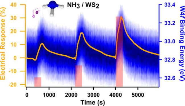
The only change in the core-level spectra is a notable shift in the binding energy. This is better observed in Figure 6a,b, where the 2D image plots of the N 1s and W 4f core-level spectra are reported simultaneously to the electrical measurements shown in Figure 5. Together with the intensity plots, two spectra (N 1s and W 4f) recorded at the beginning and on top of the third ammonia pulse are reported in Figure 6c,d. In the N 1s spectra in dry air (black spectrum), only one peak is present at about 405 eV and corresponds to the N2 gas phase. While in correspondence with the three ammonia pulses, the NH3 gas phase is detected at about 401 eV. In Figure 6c, the N 1s spectrum of the gas phase is also shown, corresponding to the gas composition of 760 ppm of NH3 gas in dry air measured without a sample in the cell. The two peaks can be easily distinguished. The N 1s from N2 and the surface W 4f peaks both show a change in the position of the peaks, in correspondence with the ammonia pulses. The binding energy shift increases with the increase in the ammonia concentration, as summarized in Figure 6e. The binding energy shift of W 4f and N 1s gas phases from the N2 gas-phase peak is also reported, obtained by peak fitting the intensity plots in Figure 6a,b. For comparison with the simultaneous APXPS measurement, the change in the resistivity, shown in Figure 5, is reported again. In the same figure, the area calculated from the N 1s core level relative to the NH3 gas phase clearly shows the ammonia pulse into dry air and perfectly matches QMS data from Figure 5.
Figure 6.

Exposure to NH3. 2D images plot of (a) N 1s and (b) W 4f in 1 mbar total pressure during three consecutive pulses of NH3 into dry air, measured with 800 eV photon energy. (c) N 1s and (d) W 4f XPS spectra extracted from (a,b), respectively, at the beginning (black, only dry air) and at the top of the third NH3 pulse. In (c), the full red gas-phase peaks are measured with the same gas composition but without a sample. (e) Position of the W 4f7/2 core-level peak (open blue circles) and N 1s of the N2 gas phase (filled yellow triangles) plotted as binding energy differences from the starting position (32.8 and 405.1 eV, respectively). The area of the N 1s peak corresponds to the NH3 gas-phase (gray shadows), and resistivity (red line, the same as Figure 5).
The shift in binding energy is very similar for both reported core levels and exactly follows the behavior of the electrical response. The fact that both gas phase and surface peaks shift is due to a change in the surface potential and not to a change in the work function, which would have caused the shift of only the gas-phase peaks.56 Therefore, the shift in binding energy is consistent with a downward band bending effect, confirming a charge transfer mechanism with electrons transferred from the gas molecules to the sensing layer.57,58
The absence of line shape modification and the change in binding energy, with its subsequent recovery to the original value, mean this is a reversible process with an unchanged oxidation state of the sample. These findings suggest a physisorption-based sensing mechanism where the molecules have small adsorption energy and large separation height, as confirmed by first-principles calculations and our DFT results.8
NO2 Exposure
The results shown so far were related to exposure to NH3. Another interesting gas for which WS2 has shown good sensing performance is NO2, an oxidizing molecule (electron acceptor). Therefore, charge transfer in the opposite way compared to NH3 is expected: electrons will be transferred from WS2 to the NO2 molecules, increasing the hole conductivity of this p-type semiconductor. In Figure 7a, the exposure to 14 ppm of NO2 in dry air is reported: the measured resistance decreased, while the photoemission peak negatively shifted, consistent with an upward band bending. While achieving the lower detection limit falls beyond the scope of this study, the possibility of detecting 14 ppm of NO2 (potentially even lower concentrations) is remarkable when compared to the state-of-the-art WS2-based sensing devices, which show a limit from few15,16 to hundreds ppm.14,20
Figure 7.

Exposure to NO2. (a) Electrical response (red curve) and position of the W 4f7/2 core-level peak (open blue circles). In gray, the 5 min pulse of NO2 at 14 ppm concentration. (b) Aggregate summary of the absolute values of the electrical response and peak position difference plotted as a function of gas concentration relative to the exposures to both gases: the open markers correspond to the data from NO2 exposure, and the filled ones correspond to the data from NH3 exposure. The dashed lines are an exponential fit of the NH3 data.
As plotted in Figure 7b, the peak position variation and electrical response exhibit an exponential correlation with the gas concentration. A plateau is observed at high ppm, indicating the active layer saturation with less available active sites for interaction. The saturation point is slightly delayed when considering the electrical response, most probably due to the sensitivity of the APXPS to the surface topmost layers of the sample. In contrast, the electrical signal is sensitive to the full depth of the active layer. On the same graph, the value for NO2 (14 ppm) is reported with open markers for comparison, yet it is excluded from the fit.
DFT Calculations
To further support our experimental findings, we performed DFT calculations to gain deeper insight into the charge transfer processes between the NH3/NO2 molecules and WS2. Density derived electrostatic and chemical (DDEC) analysis, in particular, shows that NH3 and NO2 exhibit opposite behavior when interacting with WS2. NH3 transfers 0.078 |e| to the WS2 monolayer and behaves as an electron donor, whereas the NO2 molecule is an electron acceptor and receives 0.11 |e| from the WS2 monolayer. Such charge transfer directions fully agree with the interpretation of the resistivity and APXPS measurements.
To further describe the interaction between the adsorbed gas molecules and the WS2 monolayer, the charge density difference of the adsorbed configurations was calculated as the difference between the total charge density of the gas molecule adsorbed on WS2 and the combined charge density of pristine WS2 and the isolated gas molecule in the interface geometry. The side views of the calculated charge density difference plots are shown in Figure 8. The electron accumulation and depletion regions on the isosurface are indicated in green and red, respectively. The WS2 monolayer and the gas molecules (NH3 and NO2) are not uniformly colored, thus pointing to a charge redistribution induced by the attractive interactions between the net charge on the molecule and that of the opposite sign in WS2.
Figure 8.

Side and top view of the charge density difference plot for (a) NH3/WS2 and (b) NO2/WS2. The value and direction of charge transfer are shown.
Since the shift in the binding energy measured by APXPS directly reflects the shift in the surface potential of the WS2 surface upon interaction with the gas, we also estimated this shift at the theoretical level. The DFT calculations indicate that the position of the top of the valence band does not change upon the adsorption of NH3 and NO2 on WS2 with respect to the vacuum level of pristine WS2. The shift in the binding energy observed with APXPS is thus governed by the change in the surface potential driven by two main contributions: (i) VINT: the shift of the vacuum level triggered by the interfacial dipole created upon adsorption and the associated internal charge redistribution; (ii) VMOL: the shift of the vacuum level linked to the presence of a permanent dipole moment along the normal direction in the neutral gas molecules.
The total shift in the surface potential can be deduced from the calculations by comparing the evolution of the electrostatic potential along the direction normal to the WS2 surface with and without the presence of a gas molecule, as plotted in Figure 9; to do so, the curves have to be fully aligned on the bare side of the WS2 layer. The comparison of the graphs leads to a vacuum level shift of −0.78 eV for NH3 and a shift of +0.46 eV for NO2. This is fully consistent with the different sign of the W 4f peak shift observed by APXPS upon gas exposure.
Figure 9.

Plane-averaged electrostatic potential along the normal axis for NH3 adsorbed on WS2 (a) and NO2 adsorbed on WS2 (b). The blue curve corresponds to the plane averaged electrostatic potential of pristine WS2 in the interface geometry. The zero energy is set at the valence band top. The difference between the blue and red lines (blue and green lines) corresponds to the shift in the surface potential of the bare WS2 upon adsorption of NH3 and (NO2).
Note that VMOL can be calculated independently by computing the shift of the electrostatic potential across an isolated gas molecule along the normal direction to the substrate (see Figure S3); this leads to values of −0.68 eV for NH3 and −0.13 eV for NO2. Thus, the interfacial dipole (VINT) is estimated to be −0.10 eV for NH3 and +0.59 eV for NO2. Note that we obtain remarkably similar values of the interface dipole contribution by solving Poisson’s equation (see Figure S4). Consequently, the total shift of the electrostatic potential is governed by the molecular contribution with NH3 and the charge transfer contribution with NO2.
Conclusions
Considering the absence of chemical modifications of the sample upon exposure to ammonia or nitrogen dioxide, as revealed by APXPS, we can infer that the chemoresistive response recorded is solely due to the physisorption of gas molecules on the WS2 film, followed by electronic charge transfer from (to) the molecules to (from) the WS2 film exposed to NH3 (NO2), without the involvement of sulfur vacancies, changes in the oxidation state of the tungsten atoms, or chemisorption of the gas molecules.
Due to the low adsorption energies, this process is transient and reversible since the molecules can easily desorb from the WS2 surface. This is supported by DFT calculations depicting the modification of the surface potential upon adsorption of the gas molecules on the WS2 surface.
Even though physisorption is characterized by limited charge transfer, the morphology of the WS2 films studied, consisting of a 3-dimensional, porous assembly of randomly oriented WS2 triangles, favors the presence of many sulfur edges and, therefore, explains the remarkable gas responsiveness achieved.
With this experiment, we have demonstrated the efficacy and significance of APXPS, with theoretical support, in elucidating the sensing mechanism of chemiresistors. Our focus was investigating the interaction of NH3 and NO2 with WS2 as a sensing layer, even at remarkably low NO2 concentrations. By concurrently measuring the electrical response and photoemission under relevant working pressures of unprecedented high quality, we established a correlation between the change in resistivity and the band bending of the semiconducting sensing layer, advancing beyond the current standards.
This proof-of-principle experiment establishes the foundation for future experiments using APXPS to investigate the mechanism of interaction between gas sensing active layers and target gas analytes. The designed methodology enables the tailored optimization of chemiresistor devices.
Acknowledgments
We acknowledge MAX IV Laboratory for time on Beamline HIPPIE under Proposal 20210978. Research conducted at MAX IV, a Swedish national user facility, is supported by the Swedish Research Council under contract 2018-07152, the Swedish Governmental Agency for Innovation Systems under contract 2018-04969, and Formas under contract 2019-02496. A.M. is supported by a grant from the Research Stay program, an activity of the HESEB project funded from the Initiative and Networking Fund of the Helmholtz Association. Funded in part by project no. PID2022-142451OB-C21, MICIN/AEI/10.13039/501100011033/and FEDER. E.L. is supported by the Catalan Institution for Research and Advanced Studies via the 2023 Edition of the ICREA Academia Award. The work in Mons has also been supported by the Fund for Scientific Research (FRS) of FNRS within the Consortium des Equipements de Calcul Intensif (CECI) under grant 2.5020.11 and by the Walloon Region (ZENOBE Tier-1 supercomputer) under grant 1117545. C.B and J.C. are, respectively, FNRS senior researcher and FNRS research director.
Supporting Information Available
The Supporting Information is available free of charge at https://pubs.acs.org/doi/10.1021/acssensors.4c01033.
XRD of WS2, APXPS spectra in dry air and in NH3, and DFT results about the molecular contribution to the electrostatic potential and interface dipole potential (PDF)
Author Contributions
MS: conceptualization, formal analysis, investigation, methodology, visualization, supervision, writing—original draft, and writing—review and editing. RT: methodology, investigation, and writing—review and editing. JCC: resources, investigation, and writing—review and editing. AM, GM, and AD: investigation. FEA: supervision, investigation, and writing—review and editing. AA: resources and investigation. CB: supervision, writing—original draft, writing—review and editing. EL: resources, supervision, and writing—review and editing. IA, LM, DC, and JC: formal analysis, visualization, and writing—review and editing.
The authors declare no competing financial interest.
Supplementary Material
References
- Staerz A.; Weimar U.; Barsan N. Current State of Knowledge on the Metal Oxide Based Gas Sensing Mechanism. Sens. Actuators, B 2022, 358, 131531. 10.1016/j.snb.2022.131531. [DOI] [Google Scholar]
- Donarelli M.; Ottaviano L. 2D Materials for Gas Sensing Applications: A Review on Graphene Oxide, MoS2, WS2 and Phosphorene. Sensors 2018, 18, 3638. 10.3390/s18113638. [DOI] [PMC free article] [PubMed] [Google Scholar]
- Dey A. Semiconductor Metal Oxide Gas Sensors: A Review. Mater. Sci. Eng., B 2018, 229, 206–217. 10.1016/j.mseb.2017.12.036. [DOI] [Google Scholar]
- Wang Q. H.; Kalantar-Zadeh K.; Kis A.; Coleman J. N.; Strano M. S. Electronics and Optoelectronics of Two-Dimensional Transition Metal Dichalcogenides. Nat. Nanotechnol. 2012, 7, 699–712. 10.1038/nnano.2012.193. [DOI] [PubMed] [Google Scholar]
- Yang S.; Jiang C.; Wei S. Gas Sensing in 2D Materials. Appl. Phys. Rev. 2017, 4, 021304. 10.1063/1.4983310. [DOI] [Google Scholar]
- Hozák P.; Vorokhta M. M.; Khalakhan I.; Jarkovská K.; Cibulková J.; Fitl P.; Vlček J.; Fara J.; Tomeček D.; Novotný M.; Vorokhta M. M.; Lančok J.; Matolínová I.; Vrňata M. New Insight into the Gas-Sensing Properties of CuOx Nanowires by Near-Ambient Pressure XPS. J. Phys. Chem. C 2019, 123, 29739–29749. 10.1021/acs.jpcc.9b09124. [DOI] [Google Scholar]
- Joshi N.; Hayasaka T.; Liu Y.; Liu H.; Oliveira O. N.; Lin L. A Review on Chemiresistive Room Temperature Gas Sensors Based on Metal Oxide Nanostructures, Graphene and 2D Transition Metal Dichalcogenides. Microchim. Acta 2018, 185, 213. 10.1007/s00604-018-2750-5. [DOI] [PubMed] [Google Scholar]
- Yue Q.; Shao Z.; Chang S.; Li J. Adsorption of Gas Molecules on Monolayer MoS2 and Effect of Applied Electric Field. Nanoscale Res. Lett. 2013, 8, 425. 10.1186/1556-276x-8-425. [DOI] [PMC free article] [PubMed] [Google Scholar]
- Ou J. Z.; Ge W.; Carey B.; Daeneke T.; Rotbart A.; Shan W.; Wang Y.; Fu Z.; Chrimes A. F.; Wlodarski W.; Russo S. P.; Li Y. X.; Kalantar-zadeh K. Physisorption-Based Charge Transfer in Two-Dimensional SnS 2 for Selective and Reversible NO 2 Gas Sensing. ACS Nano 2015, 9, 10313–10323. 10.1021/acsnano.5b04343. [DOI] [PubMed] [Google Scholar]
- Sharma S.; Saini R.; Gupta G.; Late D. J. Room-Temperature Highly Sensitive and Selective NH 3 Gas Sensor Using Vertically Aligned WS 2 Nanosheets. Nanotechnology 2023, 34, 045704. 10.1088/1361-6528/ac9c0c. [DOI] [PubMed] [Google Scholar]
- Paul R.; Das B.; Ghosh R. Novel Approaches towards Design of Metal Oxide Based Hetero-Structures for Room Temperature Gas Sensor and Its Sensing Mechanism: A Recent Progress. J. Alloys Compd. 2023, 941, 168943. 10.1016/j.jallcom.2023.168943. [DOI] [Google Scholar]
- Wang Z.; Bu M.; Hu N.; Zhao L. An Overview on Room-Temperature Chemiresistor Gas Sensors Based on 2D Materials: Research Status and Challenge. Composites, Part B 2023, 248, 110378. 10.1016/j.compositesb.2022.110378. [DOI] [Google Scholar]
- Li Z.; Li H.; Wu Z.; Wang M.; Luo J.; Torun H.; Hu P.; Yang C.; Grundmann M.; Liu X.; Fu Y. Advances in Designs and Mechanisms of Semiconducting Metal Oxide Nanostructures for High-Precision Gas Sensors Operated at Room Temperature. Mater. Horiz. 2019, 6, 470–506. 10.1039/C8MH01365A. [DOI] [Google Scholar]
- Perrozzi F.; Emamjomeh S. M.; Paolucci V.; Taglieri G.; Ottaviano L.; Cantalini C. Thermal Stability of WS2 Flakes and Gas Sensing Properties of WS2/WO3 Composite to H2, NH3 and NO2. Sens. Actuators, B 2017, 243, 812–822. 10.1016/j.snb.2016.12.069. [DOI] [Google Scholar]
- Liu D.; Tang Z.; Zhang Z. Comparative Study on NO2 and H2S Sensing Mechanisms of Gas Sensors Based on WS2 Nanosheets. Sens. Actuators, B 2020, 303, 127114. 10.1016/j.snb.2019.127114. [DOI] [Google Scholar]
- Alagh A.; Annanouch F. E.; Umek P.; Bittencourt C.; Sierra-Castillo A.; Haye E.; Colomer J. F.; Llobet E. CVD Growth of Self-Assembled 2D and 1D WS2 Nanomaterials for the Ultrasensitive Detection of NO2. Sens. Actuators, B 2021, 326, 128813. 10.1016/j.snb.2020.128813. [DOI] [Google Scholar]
- Han Y.; Liu Y.; Su C.; Chen X.; Li B.; Jiang W.; Zeng M.; Hu N.; Su Y.; Zhou Z.; Zhu Z. G.; Yang Z. Hierarchical WS2-WO3Nanohybrids with P-N Heterojunctions for NO2Detection. ACS Appl. Nano Mater. 2021, 4, 1626–1634. 10.1021/acsanm.0c03094. [DOI] [Google Scholar]
- Luo H.; Shi J.; Liu C.; Chen X.; Lv W.; Zhou Y.; Zeng M.; Yang J.; Wei H.; Zhou Z.; Su Y.; Hu N.; Yang Z. Design of p-p Heterojunctions Based on CuO Decorated WS 2 Nanosheets for Sensitive NH 3 Gas Sensing at Room Temperature. Nanotechnology 2021, 32, 445502. 10.1088/1361-6528/ac1800. [DOI] [PubMed] [Google Scholar]
- Li X.; Yang J.; Zhai Y.; Li X.; Quan W.; Mehrez J. A. A.; Wu J.; Liu X.; He T.; Zeng M.; Hu N.; Li B.; Wang T.; Yang Z. Ultraviolet Irradiation Stimulated NO2 Sensing Using WS2 Nanosheets Decorated with Au Nanoparticles. ACS Appl. Nano Mater. 2024, 7, 6293–6304. 10.1021/acsanm.3c06222. [DOI] [Google Scholar]
- Ko K. Y.; Lee S.; Park K.; Kim Y.; Woo W. J.; Kim D.; Song J. G.; Park J.; Kim J. H.; Lee Z.; Kim H. High-Performance Gas Sensor Using a Large-Area WS2xSe2–2x Alloy for Low-Power Operation Wearable Applications. ACS Appl. Mater. Interfaces 2018, 10, 34163–34171. 10.1021/acsami.8b10455. [DOI] [PubMed] [Google Scholar]
- Cho B.; Hahm M. G.; Choi M.; Yoon J.; Kim A. R.; Lee Y.-J.; Park S.-G.; Kwon J.-D.; Kim C. S.; Song M.; Jeong Y.; et al. Charge-Transfer-Based Gas Sensing Using Atomic-Layer MoS2. Sci. Rep. 2015, 5, 8052. 10.1038/srep08052. [DOI] [PMC free article] [PubMed] [Google Scholar]
- Feng Y.; Zhang K.; Li H.; Wang F.; Zhou B.; Fang M.; Wang W.; Wei J.; Wong H. S. P. In Situ Visualization and Detection of Surface Potential Variation of Mono and Multilayer MoS 2 under Different Humidities Using Kelvin Probe Force Microscopy. Nanotechnology 2017, 28, 295705. 10.1088/1361-6528/aa7183. [DOI] [PubMed] [Google Scholar]
- Lee S. Y.; Kim U. J.; Chung J.; Nam H.; Jeong H. Y.; Han G. H.; Kim H.; Oh H. M.; Lee H.; Kim H.; Roh Y.-G.; Kim J.; Hwang S. W.; Park Y.; Lee Y. H. Large Work Function Modulation of Monolayer MoS 2 by Ambient Gases. ACS Nano 2016, 10, 6100–6107. 10.1021/acsnano.6b01742. [DOI] [PubMed] [Google Scholar]
- Late D. J.; Huang Y.-K.; Liu B.; Acharya J.; Shirodkar S. N.; Luo J.; Yan A.; Charles D.; Waghmare U. V.; Dravid V. P.; Rao C. N. R. Sensing Behavior of Atomically Thin-Layered MoS 2 Transistors. ACS Nano 2013, 7, 4879–4891. 10.1021/nn400026u. [DOI] [PubMed] [Google Scholar]
- Jensen I. J. T.; Ali A.; Zeller P.; Amati M.; Schrade M.; Vullum P. E.; Muñiz M. B.; Bisht P.; Taniguchi T.; Watanabe K.; Mehta B. R.; Gregoratti L.; Belle B. D. Direct Observation of Charge Transfer between NOx and Monolayer MoS2 by Operando Scanning Photoelectron Microscopy. ACS Appl. Nano Mater. 2021, 4, 3319–3324. 10.1021/acsanm.1c00137. [DOI] [Google Scholar]
- Hübner M.; Koziej D.; Bauer M.; Barsan N.; Kvashnina K.; Rossell M. D.; Weimar U.; Grunwaldt J. The Structure and Behavior of Platinum in SnO 2 -Based Sensors under Working Conditions. Angew. Chem., Int. Ed. 2011, 50, 2841–2844. 10.1002/anie.201004499. [DOI] [PubMed] [Google Scholar]
- Degler D.; Pereira de Carvalho H. W.; Kvashnina K.; Grunwaldt J.-D.; Weimar U.; Barsan N. Structure and Chemistry of Surface-Doped Pt:SnO 2 Gas Sensing Materials. RSC Adv. 2016, 6, 28149–28155. 10.1039/C5RA26302F. [DOI] [Google Scholar]
- Braglia L.; Fracchia M.; Ghigna P.; Minguzzi A.; Meroni D.; Edla R.; Vandichel M.; Ahlberg E.; Cerrato G.; Torelli P. Understanding Solid-Gas Reaction Mechanisms by Operando Soft X-Ray Absorption Spectroscopy at Ambient Pressure. J. Phys. Chem. C 2020, 124, 14202–14212. 10.1021/acs.jpcc.0c02546. [DOI] [PMC free article] [PubMed] [Google Scholar]
- Zhou C.; Yang W.; Zhu H. Mechanism of Charge Transfer and Its Impacts on Fermi-Level Pinning for Gas Molecules Adsorbed on Monolayer WS2. J. Chem. Phys. 2015, 142, 214704. 10.1063/1.4922049. [DOI] [PubMed] [Google Scholar]
- Sun L.; Zhang X.; Liu F.; Shen Y.; Fan X.; Zheng S.; Thong J. T. L.; Liu Z.; Yang S. A.; Yang H. Y. Vacuum Level Dependent Photoluminescence in Chemical Vapor Deposition-Grown Monolayer MoS 2. Sci. Rep. 2017, 7, 16714–16719. 10.1038/s41598-017-15577-1. [DOI] [PMC free article] [PubMed] [Google Scholar]
- Salmeron M.; Schlogl R. Ambient Pressure Photoelectron Spectroscopy: A New Tool for Surface Science and Nanotechnology. Surf. Sci. Rep. 2008, 63, 169–199. 10.1016/j.surfrep.2008.01.001. [DOI] [Google Scholar]
- Schnadt J.; Knudsen J.; Johansson N. Present and New Frontiers in Materials Research by Ambient Pressure X-Ray Photoelectron Spectroscopy. J. Phys.: Condens. Matter 2020, 32, 413003. 10.1088/1361-648X/ab9565. [DOI] [PubMed] [Google Scholar]
- Kucharski S.; Ferrer P.; Venturini F.; Held G.; Walton A. S.; Byrne C.; Covington J. A.; Ayyala S. K.; Beale A. M.; Blackman C. Direct in Situ Spectroscopic Evidence of the Crucial Role Played by Surface Oxygen Vacancies in the O 2 -Sensing Mechanism of SnO 2. Chem. Sci. 2022, 13, 6089–6097. 10.1039/D2SC01738E. [DOI] [PMC free article] [PubMed] [Google Scholar]
- Junker B.; Favaro M.; Starr D. E.; Hävecker M.; Weimar U.; Barsan N. NAP-XPS as a New Tool for in-Situ Studies of SMOX Gas Sensors. J. Phys. D Appl. Phys. 2022, 55, 064002. 10.1088/1361-6463/ac3283. [DOI] [Google Scholar]
- Vorokhta M.; Khalakhan I.; Vondráček M.; Tomeček D.; Vorokhta M.; Marešová E.; Nováková J.; Vlček J.; Fitl P.; Novotný M.; Hozák P.; Lančok J.; Vrňata M.; Matolínová I.; Matolín V. Investigation of Gas Sensing Mechanism of SnO2 Based Chemiresistor Using near Ambient Pressure XPS. Surf. Sci. 2018, 677, 284–290. 10.1016/j.susc.2018.08.003. [DOI] [Google Scholar]
- Karagoz B.; Tsyshevsky R.; Trotochaud L.; Yu Y.; Karslıoğlu O.; Blum M.; Eichhorn B.; Bluhm H.; Kuklja M. M.; Head A. R. NO 2 Interactions with MoO 3 and CuO at Atmospherically Relevant Pressures. J. Phys. Chem. C 2021, 125, 16489–16497. 10.1021/acs.jpcc.1c02517. [DOI] [Google Scholar]
- Liu L.; Wang Y.; Guan K.; Liu Y.; Li Y.; Sun F.; Wang X.; Zhang C.; Feng S.; Zhang T. Influence of Oxygen Vacancies on the Performance of SnO2 Gas Sensing by Near-Ambient Pressure XPS Studies. Sens. Actuators, B 2023, 393, 134252. 10.1016/j.snb.2023.134252. [DOI] [Google Scholar]
- Yuan G.; Zhang H.; Cheng Y.; Zhong Y.; Zhuo Q.; Sun X. Hollow Polyhedral ZnCo 2 O 4 Superstructure as an Ethanol Gas Sensor and Sensing Mechanism Study Using near Ambient Pressure XPS. J. Mater. Chem. C 2021, 9, 14278–14285. 10.1039/D1TC03450B. [DOI] [Google Scholar]
- Minezaki T.; Krüger P.; Annanouch F. E.; Casanova-Cháfer J.; Alagh A.; Villar-Garcia I. J.; Pérez-Dieste V.; Llobet E.; Bittencourt C. Hydrogen Sensing Mechanism of WS2 Gas Sensors Analyzed with DFT and NAP-XPS. Sensors 2023, 23, 4623. 10.3390/s23104623. [DOI] [PMC free article] [PubMed] [Google Scholar]
- Blackman C. Do We Need “Ionosorbed” Oxygen Species? (Or, “A Surface Conductivity Model of Gas Sensitivity in Metal Oxides Based on Variable Surface Oxygen Vacancy Concentration”). ACS Sens. 2021, 6, 3509–3516. 10.1021/acssensors.1c01727. [DOI] [PubMed] [Google Scholar]
- Alagh A.; Annanouch F. E.; YoussefBittencourt K. A. C.; Güell F.; Martínez-Alanis P. R.; Reguant M.; Llobet E.; Llobet E. PdO and PtO Loaded WS2 Boosts NO2 Gas Sensing Characteristics at Room Temperature. Sens. Actuators, B 2022, 364, 131905. 10.1016/j.snb.2022.131905. [DOI] [Google Scholar]
- Annanouch F. E.; Haddi Z.; Vallejos S.; Umek P.; Guttmann P.; Bittencourt C.; Llobet E. Aerosol-Assisted CVD-Grown WO 3 Nanoneedles Decorated with Copper Oxide Nanoparticles for the Selective and Humidity-Resilient Detection of H 2 S. ACS Appl. Mater. Interfaces 2015, 7, 6842–6851. 10.1021/acsami.5b00411. [DOI] [PubMed] [Google Scholar]
- Berkdemir A.; Gutiérrez H. R.; Botello-Méndez A. R.; Perea-López N.; Elías A. L.; Chia C.-I.; Wang B.; Crespi V. H.; López-Urías F.; Charlier J.-C.; Terrones H.; Terrones M. Identification of Individual and Few Layers of WS2 Using Raman Spectroscopy. Sci. Rep. 2013, 3, 1755. 10.1038/srep01755. [DOI] [Google Scholar]
- Alagh A.; Annanouch F. E.; Umek P.; Bittencourt C.; Colomer J. F.; Llobet E. An Ultrasensitive Room-Temperature H2S Gas Sensor Based on 3D Assembly of Cu2O Decorated WS2 Nanomaterial. IEEE Sens. J. 2021, 21, 21212–21220. 10.1109/JSEN.2021.3103925. [DOI] [Google Scholar]
- Zhu S.; Scardamaglia M.; Kundsen J.; Sankari R.; Tarawneh H.; Temperton R.; Pickworth L.; Cavalca F.; Wang C.; Tissot H.; Weissenrieder J.; et al. HIPPIE: A New Platform for Ambient-Pressure X-Ray Photoelectron Spectroscopy at the MAX IV Laboratory. J. Synchrotron Radiat. 2021, 28, 624–636. 10.1107/s160057752100103x. [DOI] [PMC free article] [PubMed] [Google Scholar]
- Kresse G.; Furthmüller J. Efficient Iterative Schemes for Ab Initio Total-Energy Calculations Using a Plane-Wave Basis Set. Phys. Rev. B: Condens. Matter Mater. Phys. 1996, 54, 11169–11186. 10.1103/PhysRevB.54.11169. [DOI] [PubMed] [Google Scholar]
- Kresse G.; Joubert D. From Ultrasoft Pseudopotentials to the Projector Augmented-Wave Method. Phys. Rev. B: Condens. Matter Mater. Phys. 1999, 59, 1758–1775. 10.1103/PhysRevB.59.1758. [DOI] [Google Scholar]
- Perdew J. P.; Burke K.; Ernzerhof M. Generalized Gradient Approximation Made Simple. Phys. Rev. Lett. 1996, 77, 3865–3868. 10.1103/PhysRevLett.77.3865. [DOI] [PubMed] [Google Scholar]
- Heyd J.; Scuseria G. E.; Ernzerhof M. Hybrid Functionals Based on a Screened Coulomb Potential. J. Chem. Phys. 2003, 118, 8207–8215. 10.1063/1.1564060. [DOI] [Google Scholar]
- Grimme S. Semiempirical GGA-type Density Functional Constructed with a Long-range Dispersion Correction. J. Comput. Chem. 2006, 27, 1787–1799. 10.1002/jcc.20495. [DOI] [PubMed] [Google Scholar]
- Neugebauer J.; Scheffler M. Adsorbate-Substrate and Adsorbate-Adsorbate Interactions of Na and K Adlayers on Al(111). Phys. Rev. B: Condens. Matter Mater. Phys. 1992, 46, 16067–16080. 10.1103/PhysRevB.46.16067. [DOI] [PubMed] [Google Scholar]
- Limas N. G.; Manz T. A. Introducing DDEC6 Atomic Population Analysis: Part 2. Computed Results for a Wide Range of Periodic and Nonperiodic Materials. RSC Adv. 2016, 6, 45727–45747. 10.1039/C6RA05507A. [DOI] [Google Scholar]
- Manz T. A.; Limas N. G. Introducing DDEC6 atomic population analysis: part 1. Charge partitioning theory and methodology. Charge Partitioning Theory and Methodology. RSC Adv. 2016, 6, 47771–47801. 10.1039/C6RA04656H. [DOI] [PMC free article] [PubMed] [Google Scholar]
- Paolucci V.; Emamjomeh S. M.; Nardone M.; Ottaviano L.; Cantalini C. Two-Step Exfoliation of WS2 for NO2, H2 and Humidity Sensing Applications. Nanomaterials 2019, 9, 1363. 10.3390/nano9101363. [DOI] [PMC free article] [PubMed] [Google Scholar]
- Li H.; Huang M.; Cao G. Markedly Different Adsorption Behaviors of Gas Molecules on Defective Monolayer MoS 2: A First-Principles Study. Phys. Chem. Chem. Phys. 2016, 18, 15110–15117. 10.1039/C6CP01362G. [DOI] [PubMed] [Google Scholar]
- Head A. R.; Bluhm H.. Ambient Pressure X-Ray Photoelectron Spectroscopy. In Encyclopedia of Interfacial Chemistry; Elsevier, 2018; pp 13–27. [Google Scholar]
- Zhang Z.; Yates J. T. Effect of Adsorbed Donor and Acceptor Molecules on Electron Stimulated Desorption: O 2/TiO 2 (110). J. Phys. Chem. Lett. 2010, 1, 2185–2188. 10.1021/jz1007559. [DOI] [Google Scholar]
- Zhang Z.; Yates J. T. Band Bending in Semiconductors: Chemical and Physical Consequences at Surfaces and Interfaces. Chem. Rev. 2012, 112, 5520–5551. 10.1021/cr3000626. [DOI] [PubMed] [Google Scholar]
Associated Data
This section collects any data citations, data availability statements, or supplementary materials included in this article.