Abstract
Two-dimensional (2D) ferromagnetic semiconductors (FM SCs) provide an ideal platform for the development of quantum information technology in nanoscale devices. However, many developed 2D FM materials present a very low Curie temperature (TC), greatly limiting their application in spintronic devices. In this work, we predict two stable 2D transition metal chalcogenides, V3Se3X2 (X = S, Te) monolayers, by using first-principles calculations. Our results show that the V3Se3Te2 monolayer is a robust bipolar magnetic SC with a moderate bandgap of 0.53 eV, while V3Se3S2 is a direct band-gap FM SC with a bandgap of 0.59 eV. Interestingly, the ferromagnetisms of both monolayers are robust due to the V–S/Se/Te–V superexchange interaction, and TCs are about 406 K and 301 K, respectively. Applying biaxial strains, the FM SC to antiferromagnetic (AFM) SC transition is revealed at 5% and 3% of biaxial tensile strain. In addition, their high mechanical, dynamical, and thermal stabilities are further verified by phonon dispersion calculations and ab initio molecular dynamics (AIMD) calculations. Their outstanding attributes render the V3Se3Y2 (Y = S, Te) monolayers promising candidates as 2D FM SCs for a wide range of applications.
Keywords: ferromagnetic, semiconductor, high Curie temperature, spintronics
1. Introduction
With the development of device minimization processing, various two-dimensional (2D) semiconductors (SC) with large surface-to-volume ratios and intriguing electronic properties have attracted intensive attention [1,2,3,4,5,6,7,8]. Among them, the emergence of 2D ferromagnetic semiconductors (FM SCs) has drawn particular interest by combining the complementary function of SCs and FM materials, allowing the coupling and dependent control of electron charge and spin [9,10,11]. Compared with conventional electronics based on electron charge degree of freedom [12,13,14], 2D FM SCs show advantages of high energy-efficient performance, faster information operation, non-volatile data storage, etc. Unfortunately, most 2D semiconducting materials are found to be nonmagnetic due to their incompatibility between semi-conductivity and magnetism [15]. In addition, a long-range magnetic ordering in magnetism is difficult to maintain because of thermal agitation, according to the Mermin–Wagner theorem [16]. These challenges largely limit the widespread applications of 2D FM SC-based spintronics devices.
The experimental breakthroughs in 2D FM SCs were the successful preparation of the CrI3 monolayer and Cr2Ge2Te6 bilayer in 2017 [17,18]. Inspired by these achievements, a number of 2D FM SCs were fabricated and predicted by experimental and theoretical researchers, including transition-metal (TM) halides [17], TM dichalcogenides (TMDs) [19], TM chalcogenide-halide Janus complexes [20], and their various derivatives [21]. Despite the progress, most of these FM SCs possess lower than room temperature TC. For example, the TCs of the CrI3 monolayer [22] and the Cr2Ge2Te6 bilayer [23] are as low as 45 K and 63 K, respectively, which greatly limits their practical applications. Alternatively, 2D Janus TMDCs with hetero chalcogenide elements are found to show novel electronic and magnetic properties due to their broken structural symmetry [24]. In addition, robust ferromagnetic and half-metallic characters are identified for Janus FeXY (X, Y = Cl, Br, and I, X ≠ Y) monolayers [25]. The 2D VSSe was found to be a highly stable room-temperature FM SC with valley polarization feature [20]. The 2D MnSSe was revealed to be high TC FM half-metal, in which the magnetization easy axis can be tuned by hole and electron doping [26]. Research on the Janus structure then reached a high point, aiming to explore materials with better performance.
In this work, by using the first-principles method, we predict two high-temperature 2D Janus FM SCs, namely, V3Se3X2 (X = S, Te) monolayers. Both systems are predicted to be thermodynamically stable. Interestingly, the ferromagnets of both structures are found to be robust based on the V–S/Se/Te–V superexchange interaction and their TCs are about 406 K and 301 K for V3Se3S2 and V3Se3Te2, respectively. Moreover, the electronic and magnetic properties of both systems can be flexibly modulated under external in-plane biaxial strains.
2. Results and Discussion
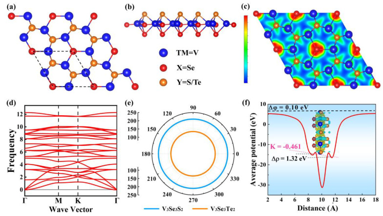
Figure 1a,b presents the crystal structure of monolayer V3Se3X2 (X = S, Te), which is a three-atomic-layer thickness incorporating V, Se, and X atoms. Their space group is P3m1, and the lattice constants are 5.76 Å and 5.95 Å for the V3Se3S2 and V3Se3Te2 monolayers, respectively, in which, the V-V and the V-Se bond lengths in the middle plane are around 3.00~3.12 Å and 2.44~2.47 Å, and the V-S/Te and V-Se bond lengths out of the middle plane are around 2.31~2.67 Å. To address the structural stability and experimental feasibility of both V3Se3X2 monolayers, we have calculated their cohesive energies (Ecoh) and formation energies (Ef) based on the following equations:
| (1) |
| (2) |
Figure 1.
The (a) top view and (b) side view of the V3Se3S2 (V3Se3Te2) monolayer. (c) The calculated electron localization function (ELF) of the V3Se3S2 monolayer for the (001) plane. (d) Phonon dispersion spectrum of V3Se3S2 monolayer. (e) Young’s modulus of V3Se3S2 (Blue) and V3Se3Te2 (Orange). (f) Average electrostatic potential of the V3Se3S2 monolayer.
Here, EV3Se3X2, μV, μSe, and μY are the total energy of V3Se3X2 monolayers, and the energies of V, Se, and S/Te atoms in their bulk crystals, respectively. EV, ESe, and EX are the energies of isolated V, Se, and S/Te atoms. The calculated Ecohs of both systems are −4.96 eV/atom and −4.52 eV/atom, respectively, comparable to that of the MoS2 (−4.53 eV/atom) and MoSe2 (−5.07 eV/atom) monolayers [27]. In addition, the Efs are −0.99 eV and −0.83 eV for V3Se3S2 and V3Se3Te2, respectively; the negative values ensure their fabrication feasibility in the experiment. Figure 1c shows the electron localization function (ELF) of the V3Se3S2 monolayer, from which we can see that the electrons are mainly delocalized around each atom, indicating their obvious ionic characters. The average electrostatic potential and charge density difference (CDD) plot of the V3Se3S2 monolayer is shown in Figure 1f. Clearly, the electrostatic potential of the S atom layer is greater than that of Se atom layer, due to the fact that the electronegativity of the S atom is greater than that of the Se atom. As a result, more electrons are found to be transferred from V atoms to S atoms than Se atoms.
The phonon spectra of the V3Se3S2 and V3Se3Te2 monolayers are illustrated in Figure 1d and Figure S1 in the Supporting Information (SI); the absence of imaginary frequencies in the Brillouin zone confirms the dynamical stabilities of both systems. In addition, the thermal stability of the V3Se3X2 (X = S, Te) monolayers is assessed by AIMD simulations at 300 K for 6 ps. As illustrated in Figure S2, the energies of the V3Se3X2 (X = S, Te) monolayers fluctuate within a narrow range during the simulation, and the final snapshot demonstrates that the structures remain well-preserved, indicating excellent thermal stability. Additionally, the mechanical stabilities for both systems are evaluated by calculating Young’s modulus and the Poisson ratio. The calculated elastic constants for the V3Se3S2/V3Se3Te2 monolayers are C11 = 247.90/193.33 N/m, C12 = 96.92/106.56 N/m, C22 = 247.90/193.33 N/m, and C66 = 75.49/43.38 N/m, respectively, which satisfy the Born stability criterion (C11, C66 > 0, C11–C22 > 0 and C11 + 2C12 > 0), indicating their mechanical stabilities. Young’s modulus and Poisson’s ratio as a function of θ angle (the angle between a certain direction and x-axis) are shown in Figure S3 for both the monolayers. It is found that Young’s modulus for the V3Se3S2 and V3Se3Te2 monolayers are isotropic with Young’s modulus for 210.01 N/m2 and 134.59 N/m2, respectively; in contrast, Poisson’s ratio for both systems is anisotropic.
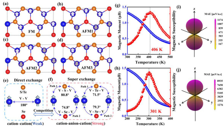
To determine the magnetic ground states of both V3Se3X2 (X = S, Te) monolayers, four magnetic configurations, namely, FM, AFM1, AFM2, and AFM3 are considered, as depicted in Figure 2a–d. Upon comparison, the FM orderings are the favored magnetic states for all the structures, which are lower in energy than AFM1, AFM2, and AFM3 by 0.080, 0.064, and 0.044 eV/atom, respectively, for V3Se3S2 and by 0.064, 0.046, and 0.026 eV/atom for V3Se3Te2. The FM ordering in both V3Se3S2 and V3Se3Te2 monolayers originate from the competition between direct and superexchange interactions (see Figure 2e,f). Direct exchange interactions are based on the overlap of wave functions between two neighboring magnetic ions, which usually leads to AFM coupling. [28] As the distance between two neighboring V atoms is as long as 3.00 and 3.12 Å, longer than that in bulk V (2.62 Å), the direct exchange interactions in both systems are very weak. On the other hand, the superexchange paths are mediated by X or Y atoms (Path 1, 2), as shown in Figure 2f, in which the V-Se-V/V-Y-V angles are around 80° and 75°, close to 90°. Therefore, the superexchange interactions determine the FM couplings of magnetic ions according to the Goodenough–Kanamori–Anderson (GKA) rule. Considering the Coulomb exchange interaction between S/Te p orbitals and the fact that the bond angle of V(I)–S/Te–V(II) is 80.8° in V3Se3S2 and 71.5° in V3Se3Te2 (relatively close to 90°), it can be inferred that the superexchange interaction brings a strong FM order [29,30]. As shown in Figure 2f, there are two kinds of V–Se–V/V-Y-V superexchange coupling pathways in each monolayer (Paths 1, 2) due to the presence of Se and Y elements. In V3Se3S2, the electrons mainly hop between V(I) dx2/V(II) dz2 via S p states, as shown in Figure 2a,b, which implies that electrons favor path 1. In V3Se3Te2, the electrons mainly hop between V(I) dx2/V(II) dz2 via Te p states, as shown in Figure 2c,d, implying path 1 is again more favored.
Figure 2.
(a–d) FM and AFM orderings. (e,f) illustrations of the V–V direct-exchange, V–S/Se/Te–V superexchange. The magnetic moment and Magnetic susceptibility of the V atom as a function of temperature for the (g) V3Se3S2 and (h) V3Se3Te2 monolayer, respectively. The magnetocrystalline anisotropy energy (MAE) for (i) V3Se3S2 and (j) V3Se3Te2 monolayer.
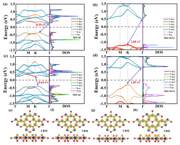
To further investigate the electronic properties of both V3Se3X2 monolayers, we have calculated the spin-resolved band structures and density of states (DOS) (Figure 3a–d). Notably, the V3Se3S2 monolayer is an FM SC with a direct bandgap of 0.59 eV, while the V3Se3Te2 monolayer exhibits an FM SC character with an indirect gap of 0.53 eV. Of particular interest, the conduction band minimum (CBM) and the valence band maximum (VBM) of the V3Se3Te2 monolayer are fully spin-polarized and occupied with opposite spin electrons, indicating a typical bipolar magnetic semiconductor (BMS) feature, as shown in Figure 3c,d [31,32,33]. As can be seen from the DOS in Figure 3a,b, the VBM and CBM are both mainly contributed to by the dx2–dz2 orbits of the V atom and p orbits of S and Te, respectively.
Figure 3.
Bands and DOS of SL V3Se3S2 in (a) spin-up and (b) spin-down channels. Bands and DOS of SL V3Se3Te2 in (c) spin-up and (d) spin-down channels. (e) CBM and (f) VBM of SL V3Se3S2. (g) CBM and (h) VBM of SL V3Se3Te2.
Generally, the Curie temperature (TC) also strongly correlates with the magnetic anisotropic energy (MAE), while it is also the key to the practical application of materials in spintronics. We use the classic Heisenberg model to investigate the magnetic couplings [34,35], the spin Hamiltonian can be considered as
| (3) |
Here, E0 is the energy without considering the interaction between magnetic atoms V. J1, J2, and J3 represent the first-nearest, second-nearest, and third-nearest spin exchange coupling parameters. Si, Sj, Sk, and Su stand for the spin vector, and Siz is the spin component. A is an anisotropy energy parameter [28,32,36]. The values of J1, J2, and J3 are computed to be 14.14, 36.16, and 5.14 meV for V3Se3S2 and 3.80 meV, 38.76 meV, and 5.98 meV for V3Se3Te2, respectively. A 10 × 10 supercell and periodic boundary conditions are adopted for the MC simulation. The magnetic moment and magnetic susceptibility are mapped out as functions of temperature in Figure 2g,h. The estimated transition temperatures for SL V3Se3S2 and V3Se3Te2 monolayers are ~406 K and ~301 K, respectively, which are higher than those of CrX3 (X = Cl, Br, I) monolayers [18,37,38] and the Cr2Ge2Te6 bilayer [17]. The main reason for a relatively high TC is the large positive magnetic exchange parameter and large MAE, which is also inseparable from the strong hybridization between V and the Te/Se/S atom.
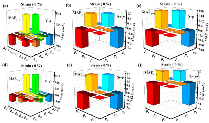
The MAEs are calculated to check the magnetic easy axis of each system as EMAE = |Ein-plane − Eout-of-plane|, which is defined as the difference between the energy of in-plane and out-plane magnetization directions. As shown in Figure 2e,f, it is found that the MAE values of V3Se3S2 and V3Se3Te2 are 196 and 1489 μeV per V atom, larger than that of CrS2 (88.5 μeV per Cr) and CrSe2 (664.0 μeV per Cr) [13]. Their magnetization directions are both in-plane, such large MAEs have rarely been observed in 2D magnetic materials. To further analyze the origin of such large MAEs, orbital resolved MAEs are displayed in Figure 4a–f, illustrating that for the V3Se3S2 monolayer, the coupling strength between the py and pz orbitals of the Se atom is the largest, next is the coupling between the dxz and V dz2 orbitals of the V atom. It can be seen that the Se pz orbital has a big influence on MAE, contributing to the negative part. In addition, the coupling strength between the Se py and Se pz orbitals is also strong with a positive value, but slightly weaker than that of the Se pz orbitals. For the V3Se3Te2 monolayer, the Te pz orbital makes the biggest contribution to the MAE, with the coupling between the Se py and Se pz orbitals coming next. As for the V d orbitals, it is the coupling of the dz2 and dxz orbitals that dominates, similar to that of the V3Se3S2 monolayer. However, the value is relatively small compared to that of the Se p and Te p orbitals, making little impact on the total MAE value.
Figure 4.
Orbital resolved MAE for (a–c) V3Se3S2 and (d–f) V3Se3Te2, respectively.
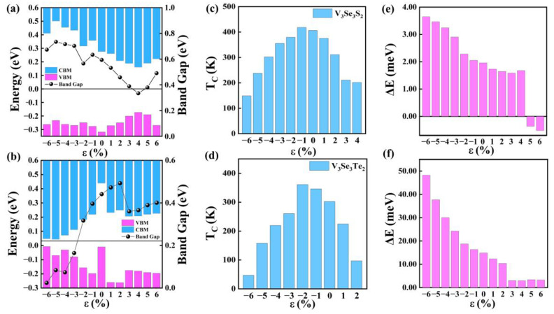
Furthermore, the effect of biaxial strains on the electronic and magnetic properties of V3Se3X2 monolayers is explored (see Figures S4 and S5). It is clear that the V3Se3S2 monolayer keeps the FM SC character in the range from −6% compressive strain to 4% tensile strain, and, under −5% and 6% tensile strain, it is changed to be an AFM BMS (see Figure S4). On the other hand, the V3Se3Te2 monolayer transitioned to be an AFM SC under 3% tensile strain (see Figure S5). Moreover, the band gap of the V3Se3S2 monolayer decreases with the external strains, ranging from −6% to 4%, and goes up slightly under tensile strains, from 4% to 6%, where the VBM experiences a little fluctuation and the CBM gets closer to the Fermi surface (see Figure 5a and Figure S4). For the V3Se3Te2 monolayer, the FM BMS property is maintained under strains from −6% to 2%; remarkably, the V3Se3Te2 monolayer undergoes a FM SC to AFM SC transition under 3% tensile strain (see Figure S5). Unlike the V3Se3S2 monolayer, the band gap of the V3Se3Te2 monolayer increases monotonously with the external strain, where the VBM and CBM get away from the Fermi surface (see Figure 5b).
Figure 5.
Band alignment scheme VBM of the (a) V3Se3S2 monolayer and (b) V3Se3S2 monolayer. (c,d) Curie temperature (TC) of the V3Se3S2 and V3Se3Te2 monolayers under different strains. MAE = Eout-plane − Ein-plane of the (e) V3Se3Te2 monolayer and (f) V3Se3Te2 monolayer plotted as a function of strain.
Finally, the influence of biaxial strains on the Curie temperature (TC) of the V3Se3S2 and V3Se3Te2 monolayers is also studied. It is observed that the TCs of both materials decrease under tensile strain, while they initially increase and then decrease under compressive strain (see Figure 5c,d). Notably, the TCs of the V3Se3S2 and V3Se3Te2 monolayers reach 418 K and 361 K when subjected to −1% and −2% compressive strains, respectively. This behavior demonstrates the tunability of the electronic properties of V3Se3Y2 (Y = S, Te) monolayers through strain engineering, thereby enhancing their potential applications in spintronic devices. Moreover, the variation of the magnetic anisotropy energies (MAE) are analyzed and presented in Figure 5e,f. It is observed that the MAE of V3Se3S2 consistently decreases within the range of −6% to 3% strain and slightly goes up at 4% strain. However, it goes below 0 meV at 5% to 6%, owing to the transition from FM SC to AFM SC. The MAE of V3Se3Te2 experiences a sharper decrease when subjected to strains from −6% to 2% and experiences a sudden decrease upon reaching a tensile strain of 3% due to the phase transition from FM SC to AFM SC.
3. Computational Methods
All the calculations are performed via the density functional theory (DFT) as implemented in the Vienna ab initio simulation package (VASP) [39]. The Perdew–Burke–Ernzerhof (PBE) [40] method based on the generalized gradient approximation (GGA) [41,42] is used to treat the exchange-correlation functional, and the electronic interaction is treated by the projector augmented wave (PAW) method [43]. To consider the Coulomb and exchange interaction of V 3d electrons, the PBE+U with U = 3 eV is adopted. The plane-wave energy cutoff is set to 500 eV, and the vacuum layer of 20 Å is employed for the studied systems to eliminate adjacent layer interactions. The geometries are fully relaxed until the force and energy convergence are less than 0.01 eV/Å and 10−6 eV, respectively. A Γ-centered k mesh of 12 × 12 × 1 is used for geometry optimization calculations. The Curie temperature (TC) of both monolayers is calculated by using the EspinS package [44], in which 10 × 10 × 1 lattices are adopted in the Monte Carlo (MC) simulations, and the spins are randomly rotated in the space. A 3 × 3 × 1 supercell of the V3Se3S2 and V3Se3Te2 monolayers are used to calculate the phonon dispersion spectrum by the PHONOPY code based on the density functional perturbation theory [45].
4. Conclusions
In summary, two types of 2D intrinsic FM SC materials, V3Se3S2 and V3Se3Te2 monolayers, are predicted by density functional theory calculations. Both of them are revealed to have good thermal, dynamic, and mechanical stabilities. Our results show that V3Se3S2 and V3Se3Te2 monolayers show robust ferromagnetism and above room temperature TC of 406 K and 301 K, respectively. The robust ferromagnetic properties are induced by the V–S/Se/Te–V superexchange interaction. V3Se3S2 monolayer is BMS with band gap of 0.59 eV, and V3Se3Te2 monolayer is an indirect band semiconductor with the band gap of 0.53 eV. When biaxial strain is introduced, a FM SC to AFM SC phase transition is found for both systems with the transition point at 5% and 3% tensile strain for the V3Se3S2 and V3Se3Te2 monolayers, respectively. Our results provide an effective method for designing promising candidates for FM SCs, which also provide opportunities for future spintronic research and applications.
Acknowledgments
We thank the computational resources at Yangzhou University. Z. J. Wang, A. H. Qureshi, and Y. Y. Duan contributed equally to this work.
Supplementary Materials
The following supporting information can be downloaded at: https://www.mdpi.com/article/10.3390/molecules29163915/s1, Figure S1: Phonon spectra of (a) V3Se3S2 and (b) V3Se3Te2; Figure S2: MD simulation was performed for geometric snapshot of the (a) V3Se3S2 and (b) V3Se3Te2 monolayer at 300 K for 6 ps; Figure S3: Young’s modules of (a) V3Se3S2 and (b) V3Se3Te2 respectively and Poisson’s ratio of (c) V3Se3S2 and (d) V3Se3Te2; Figure S4: Band structures of V3Se3S2 under biaxial strain from −6%~6%; Figure S5: Band structures of V3Se3Te2 under biaxial strain from −6%.
Author Contributions
Data curation, Z.W., A.H.Q., Y.L. (Yujie Liu) and J.Z.; writing—original draft preparation, Z.W., A.H.Q., Y.D. and J.L.; writing—review and editing, Y.W. and T.G.; supervision, X.Z. and Y.L. (Yongjun Liu); project administration—Y.W., T.G. and X.Z. All authors have read and agreed to the published version of the manuscript.
Institutional Review Board Statement
Not applicable.
Informed Consent Statement
Not applicable.
Data Availability Statement
The data presented in this study are available on request from the corresponding author.
Conflicts of Interest
The authors declare no conflicts of interest.
Funding Statement
This research received no external funding.
Footnotes
Disclaimer/Publisher’s Note: The statements, opinions and data contained in all publications are solely those of the individual author(s) and contributor(s) and not of MDPI and/or the editor(s). MDPI and/or the editor(s) disclaim responsibility for any injury to people or property resulting from any ideas, methods, instructions or products referred to in the content.
References
- 1.Geim A.K., Novoselov K.S. The rise of graphene. Nat. Mater. 2007;6:183–191. doi: 10.1038/nmat1849. [DOI] [PubMed] [Google Scholar]
- 2.Jiang S., Li L., Wang Z., Shan J., Mak K.F. Spin tunnel field-effect transistors based on two-dimensional van der Waals heterostructures. Nat. Electron. 2019;2:159–163. doi: 10.1038/s41928-019-0232-3. [DOI] [Google Scholar]
- 3.Lembke D., Bertolazzi S., Kis A. Single-Layer MoS2 Electronics. Acc. Chem. Res. 2015;48:100–110. doi: 10.1021/ar500274q. [DOI] [PubMed] [Google Scholar]
- 4.Li L., Yu Y., Ye G.J., Ge Q., Ou X., Wu H., Feng D., Chen X.H., Zhang Y. Black phosphorus field-effect transistors. Nat. Nanotechnol. 2014;9:372–377. doi: 10.1038/nnano.2014.35. [DOI] [PubMed] [Google Scholar]
- 5.Li X., Wu X. Two-dimensional monolayer designs for spintronics applications. WIREs Comput. Mol. Sci. 2016;6:441–455. doi: 10.1002/wcms.1259. [DOI] [Google Scholar]
- 6.Liu S., Yin H., Singh D.J., Liu P.-F. Ta4SiTe4: A possible one-dimensional topological insulator. Phys. Rev. B. 2022;105:195419. doi: 10.1103/PhysRevB.105.195419. [DOI] [Google Scholar]
- 7.Novoselov K.S., Geim A.K., Morozov S.V., Jiang D., Zhang Y., Dubonos S.V., Grigorieva I.V., Firsov A.A. Electric Field Effect in Atomically Thin Carbon Films. Science. 2004;306:666–669. doi: 10.1126/science.1102896. [DOI] [PubMed] [Google Scholar]
- 8.Jiang L., Marconcini P., Hossian M.S., Qiu W., Evans R., Macucci M., Skafidas E. A tight binding and study of monolayer stanene. Sci. Rep. 2017;7:12069. doi: 10.1038/s41598-017-12281-y. [DOI] [PMC free article] [PubMed] [Google Scholar]
- 9.Chappert C., Fert A., Van Dau F.N. The emergence of spin electronics in data storage. Nat. Mater. 2007;6:813–823. doi: 10.1038/nmat2024. [DOI] [PubMed] [Google Scholar]
- 10.Boeck J.D., Roy W.V., Das J., Motsnyi V., Liu Z., Lagae L., Boeve H., Dessein K., Borghs G. Technology and materials issues in semiconductor-based magnetoelectronics. Semicond. Sci. Technol. 2002;17:342. doi: 10.1088/0268-1242/17/4/307. [DOI] [Google Scholar]
- 11.Tomasz D. Ferromagnetic semiconductors. Semicond. Sci. Technol. 2002;17:377. [Google Scholar]
- 12.Jansen R. Silicon spintronics. Nat. Mater. 2012;11:400–408. doi: 10.1038/nmat3293. [DOI] [PubMed] [Google Scholar]
- 13.Xiao G., Xiao W.-Z., Chen Q., Wang L.-L. Novel two-dimensional ferromagnetic materials CrX2 (X = O, S, Se) with high Curie temperature. J. Mater. Chem. C. 2022;10:17665–17674. doi: 10.1039/D2TC03711D. [DOI] [Google Scholar]
- 14.Ohno H. Making Nonmagnetic Semiconductors Ferromagnetic. Science. 1998;281:951–956. doi: 10.1126/science.281.5379.951. [DOI] [PubMed] [Google Scholar]
- 15.Bai Y., Shi R., Wu Y., Wang B., Zhang X. Cr2XTe4 (X = Si, Ge) monolayers: A new type of two-dimensional high-TC Ising ferromagnetic semiconductors with a large magnetic anisotropy. J. Phys. Condens. Matter. 2022;34:384001. doi: 10.1088/1361-648X/ac7f16. [DOI] [PubMed] [Google Scholar]
- 16.Mermin N.D., Wagner H. Absence of Ferromagnetism or Antiferromagnetism in One- or Two-Dimensional Isotropic Heisenberg Models. Phys. Rev. Lett. 1966;17:1133–1136. doi: 10.1103/PhysRevLett.17.1133. [DOI] [Google Scholar]
- 17.Gong C., Li L., Li Z., Ji H., Stern A., Xia Y., Cao T., Bao W., Wang C., Wang Y., et al. Discovery of intrinsic ferromagnetism in two-dimensional van der Waals crystals. Nature. 2017;546:265–269. doi: 10.1038/nature22060. [DOI] [PubMed] [Google Scholar]
- 18.Huang B., Clark G., Navarro-Moratalla E., Klein D.R., Cheng R., Seyler K.L., Zhong D., Schmidgall E., McGuire M.A., Cobden D.H., et al. Layer-dependent ferromagnetism in a van der Waals crystal down to the monolayer limit. Nature. 2017;546:270–273. doi: 10.1038/nature22391. [DOI] [PubMed] [Google Scholar]
- 19.Wang Q.H., Kalantar-Zadeh K., Kis A., Coleman J.N., Strano M.S. Electronics and optoelectronics of two-dimensional transition metal dichalcogenides. Nat. Nanotechnol. 2012;7:699–712. doi: 10.1038/nnano.2012.193. [DOI] [PubMed] [Google Scholar]
- 20.Zhang C., Nie Y., Sanvito S., Du A. First-Principles Prediction of a Room-Temperature Ferromagnetic Janus VSSe Monolayer with Piezoelectricity, Ferroelasticity, and Large Valley Polarization. Nano Lett. 2019;19:1366–1370. doi: 10.1021/acs.nanolett.8b05050. [DOI] [PubMed] [Google Scholar]
- 21.Hu T., Jia F., Zhao G., Wu J., Stroppa A., Ren W. Intrinsic and anisotropic Rashba spin splitting in Janus transition-metal dichalcogenide monolayers. Phys. Rev. B. 2018;97:235404. doi: 10.1103/PhysRevB.97.235404. [DOI] [Google Scholar]
- 22.An M., Zhang Y., Chen J., Zhang H.-M., Guo Y., Dong S. Tuning Magnetism in Layered Magnet VI3: A Theoretical Study. J. Phys. Chem. C. 2019;123:30545–30550. doi: 10.1021/acs.jpcc.9b08706. [DOI] [Google Scholar]
- 23.Tian Y., Gray M.J., Ji H., Cava R.J., Burch K.S. Magneto-elastic coupling in a potential ferromagnetic 2D atomic crystal. 2D Mater. 2016;3:025035. doi: 10.1088/2053-1583/3/2/025035. [DOI] [Google Scholar]
- 24.Lu A.-Y., Zhu H., Xiao J., Chuu C.-P., Han Y., Chiu M.-H., Cheng C.-C., Yang C.-W., Wei K.-H., Yang Y., et al. Janus monolayers of transition metal dichalcogenides. Nat. Nanotechnol. 2017;12:744–749. doi: 10.1038/nnano.2017.100. [DOI] [PubMed] [Google Scholar]
- 25.Li R., Jiang J., Shi X., Mi W., Bai H. Two-Dimensional Janus FeXY (X, Y = Cl, Br, and I, X ≠ Y) Monolayers: Half-Metallic Ferromagnets with Tunable Magnetic Properties under Strain. ACS Appl. Mater. Interfaces. 2021;13:38897–38905. doi: 10.1021/acsami.1c10304. [DOI] [PubMed] [Google Scholar]
- 26.Chen Y., Fan Q., Liu Y., Yao G. Electrically tunable magnetism and unique intralayer charge transfer in Janus monolayer MnSSe for spintronics applications. Phys. Rev. B. 2022;105:195410. doi: 10.1103/PhysRevB.105.195410. [DOI] [Google Scholar]
- 27.Sun X., Liu X., Yin J., Yu J., Li Y., Hang Y., Zhou X., Yu M., Li J., Tai G., et al. Two-Dimensional Boron Crystals: Structural Stability, Tunable Properties, Fabrications and Applications. Adv. Funct. Mater. 2017;27:1603300. doi: 10.1002/adfm.201603300. [DOI] [Google Scholar]
- 28.Zhang X., Wang B., Guo Y., Zhang Y., Chen Y., Wang J. High Curie temperature and intrinsic ferromagnetic half-metallicity in two-dimensional Cr3X4 (X = S, Se, Te) nanosheets. Nanoscale Horiz. 2019;4:859–866. doi: 10.1039/C9NH00038K. [DOI] [Google Scholar]
- 29.Anderson P.W. New Approach to the Theory of Superexchange Interactions. Phys. Rev. 1959;115:2–13. doi: 10.1103/PhysRev.115.2. [DOI] [Google Scholar]
- 30.Goodenough J.B. Theory of the Role of Covalence in the Perovskite-Type Manganites [La, M(II)]MnO3. Phys. Rev. 1955;100:564–573. doi: 10.1103/PhysRev.100.564. [DOI] [Google Scholar]
- 31.Li X., Wu X., Li Z., Yang J., Hou J.G. Bipolar magnetic semiconductors: A new class of spintronics materials. Nanoscale. 2012;4:5680–5685. doi: 10.1039/c2nr31743e. [DOI] [PubMed] [Google Scholar]
- 32.Zhao C.-X., Liu J.-N., Li B.-Q., Ren D., Chen X., Yu J., Zhang Q. Multiscale Construction of Bifunctional Electrocatalysts for Long-Lifespan Rechargeable Zinc–Air Batteries. Adv. Funct. Mater. 2020;30:2003619. doi: 10.1002/adfm.202003619. [DOI] [Google Scholar]
- 33.Zhong C., Wu W., He J., Ding G., Liu Y., Li D., Yang S.A., Zhang G. Two-dimensional honeycomb borophene oxide: Strong anisotropy and nodal loop transformation. Nanoscale. 2019;11:2468–2475. doi: 10.1039/C8NR08729F. [DOI] [PubMed] [Google Scholar]
- 34.Wang B., Zhang X., Zhang Y., Yuan S., Guo Y., Dong S., Wang J. Prediction of a two-dimensional high-TC f-electron ferromagnetic semiconductor. Mater. Horiz. 2020;7:1623–1630. doi: 10.1039/D0MH00183J. [DOI] [Google Scholar]
- 35.Wang B., Zhang Y., Ma L., Wu Q., Guo Y., Zhang X., Wang J. MnX (X = P, As) monolayers: A new type of two-dimensional intrinsic room temperature ferromagnetic half-metallic material with large magnetic anisotropy. Nanoscale. 2019;11:4204–4209. doi: 10.1039/C8NR09734H. [DOI] [PubMed] [Google Scholar]
- 36.Guo Y., Zhang Y., Yuan S., Wang B., Wang J. Chromium sulfide halide monolayers: Intrinsic ferromagnetic semiconductors with large spin polarization and high carrier mobility. Nanoscale. 2018;10:18036–18042. doi: 10.1039/C8NR06368K. [DOI] [PubMed] [Google Scholar]
- 37.Zhang Z., Shang J., Jiang C., Rasmita A., Gao W., Yu T. Direct Photoluminescence Probing of Ferromagnetism in Monolayer Two-Dimensional CrBr3. Nano Lett. 2019;19:3138–3142. doi: 10.1021/acs.nanolett.9b00553. [DOI] [PubMed] [Google Scholar]
- 38.Cai X., Song T., Wilson N.P., Clark G., He M., Zhang X., Taniguchi T., Watanabe K., Yao W., Xiao D., et al. Atomically Thin CrCl3: An In-Plane Layered Antiferromagnetic Insulator. Nano Lett. 2019;19:3993–3998. doi: 10.1021/acs.nanolett.9b01317. [DOI] [PubMed] [Google Scholar]
- 39.Kresse G., Furthmüller J. Efficient iterative schemes for ab initio total-energy calculations using a plane-wave basis set. Phys. Rev. B. 1996;54:11169–11186. doi: 10.1103/PhysRevB.54.11169. [DOI] [PubMed] [Google Scholar]
- 40.Perdew J.P., Burke K., Ernzerhof M. Generalized Gradient Approximation Made Simple. Phys. Rev. Lett. 1996;77:3865–3868. doi: 10.1103/PhysRevLett.77.3865. [DOI] [PubMed] [Google Scholar]
- 41.Wang L., Maxisch T., Ceder G. Oxidation energies of transition metal oxides within the GGA + U framework. Phys. Rev. B. 2006;73:195107. doi: 10.1103/PhysRevB.73.195107. [DOI] [Google Scholar]
- 42.Jain A., Hautier G., Ong S.P., Moore C.J., Fischer C.C., Persson K.A., Ceder G. Formation enthalpies by mixing GGA and GGA + U calculations. Phys. Rev. B. 2011;84:045115. doi: 10.1103/PhysRevB.84.045115. [DOI] [Google Scholar]
- 43.Blöchl P.E. Projector augmented-wave method. Phys. Rev. B. 1994;50:17953–17979. doi: 10.1103/PhysRevB.50.17953. [DOI] [PubMed] [Google Scholar]
- 44.Rezaei N., Alaei M., Akbarzadeh H. ESpinS: A program for classical Monte-Carlo simulations of spin systems. Comput. Mater. Sci. 2022;202:110947. doi: 10.1016/j.commatsci.2021.110947. [DOI] [Google Scholar]
- 45.Togo A., Oba F., Tanaka I. First-principles calculations of the ferroelastic transition between rutile-type and CaCl2-type SiO at high pressures. Phys. Rev. B. 2008;78:134106. doi: 10.1103/PhysRevB.78.134106. [DOI] [Google Scholar]
Associated Data
This section collects any data citations, data availability statements, or supplementary materials included in this article.
Supplementary Materials
Data Availability Statement
The data presented in this study are available on request from the corresponding author.


