Abstract
Quantum-dot cellular automata (QCA) has recently been highlighted as a next-generation circuit design technology that can replace existing CMOS technology due to its advantages of maintaining very low energy consumption, small area requirements, and low latency. In this study, we propose a demultiplexer (DeMux), which is essential for safe data distribution in reliable communication network and signal routing. Our DeMux is designed based on single-layer cell interaction and maximizes area utilization while using the minimum number of cells and low area. We show that the proposed unit DeMux is easily scalable using multi-layer crossovers. The proposed cell interaction-based operation was physically verified using the potential energy of electrons, and all circuits were simulated using QCADesigner and QCADesigner-E to confirm normal operation and excellent performance. The design cost of the proposed DeMux is measured in two ways: design cost using area and delay, and design cost using energy dissipation and delay.
Keywords: Nano communication, Quantum-dot cellular automata, Demultiplexer, Physical verification, Energy dissipation, Information reliability
1. Introduction
Moore's Law, which states that the amount of data that can be stored in a microchip doubles every two years, is no longer applicable to nanoscale devices, and quantum mechanics dominates the physical phenomena of increasingly smaller hardware [1,2]. Devices relying on existing CMOS technology are experiencing increasing demand for nanoscale computational systems to minimize physical resistance to solve problems of power and information loss [3].
Quantum-dot cellular automata (QCA) is emerging as an alternative to overcome the various limitations of existing CMOS. This technology uses the Coulomb repulsion of electrons within quantum dots to express two values, 0 and 1, within one cell. Unlike existing hardware technology that only has a 1-bit value in one register, it is designed to allow overlapping of values within one cell. In addition, by using a nano-scale small size, it is efficient in space use and has a fast switching speed, resulting in low latency [4].
The standard cell of QCA, developed by Tougaw and Lent in 1993, consisted of five quantum dots, four at each corner and one quantum dot in the center. As two electrons move diagonally from the central quantum dot due to Coulomb repulsion, the polarization value is defined as +1 or −1. The most widely used recent QCA model uses four quantum dots, and electrons move between each two quantum dots by tunneling. Using these properties, various QCA-based circuits are being designed and are aiming for ultra-high-speed and ultra-small circuits [5,6].
Meanwhile, a demultiplexer (DeMux) has many applications in digital systems, including memory decoding, signal routing, and communication systems. They are also used in computer networks, where they are used to split a single data stream into multiple transmission channels. The DeMux performs the role of a distributor that divides the input value by designating the output line according to the input selection signal. It is a digital circuit used with a multiplexer for data communication and signal routing. Recently, as communication equipment has rapidly become lighter and more compact, small and fast nano-level circuits are being developed. In addition, continuous design developments are being made in circuits that minimize energy dissipation and are highly scalable [[7], [8], [9]]. Therefore, the key objective of the proposed research is to minimize the circuit design cost. We aim to design a DeMux circuit with optimal space-time complexity and energy dissipation suitable for nanodevices.
This work is structured as follows: Section 2 reviews the basic background knowledge of QCA and the existing 1-to-2 DeMux and 1-to-4 DeMux structures, and Section 3 introduces the proposed coplanar cell interaction 1-to-2 DeMux, and provides a physical Proof is provided. Additionally, a 1-to-4 DeMux with multi-layer crossover is proposed. Typical excellent circuits and ours are simulated using QCADesigner and QCADesigner-E and analyzed and compared in various performance aspects including two types of design costs in Section 4. Finally, the conclusion is made in Section 5.
2. Related works
In this section, we briefly look at QCA cells and gates, and review existing 1-to-2 DeMux circuits.
2.1. Background of QCA
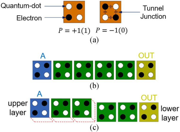
The first QCA standard cell proposed by Tougaw and Lent in 1993 had five quantum dots. It was located at the corners and the center of a square. QCA encodes binary information according to the positions of individual electrons, as shown in Fig. 1(a).
Fig. 1.
QCA cells: (a) regular cells with polarization “+1” and “-1”; (b) wiring on single layer; (c) wiring between different layers.
The cell consists of two mobile electrons that can tunnel between quantum dots. Due to the potential barrier between cells, tunneling of electrons out of the cell is impossible, and two electrons can be activated in one cell, and are always located at the quantum dot at the diagonal corner due to the Coulomb repulsion of negative charges. Fig. 1(b) shows the wiring structure for value transfer on the same plane. When wiring connects cells in succession, the polarization continues to be transmitted, and Fig. 1(c) shows that wiring in a multi-layer structure is done similarly [10,11].
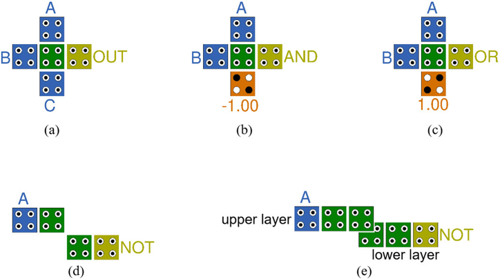
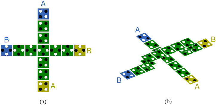
Fig. 2(a) shows a majority gate that takes three inputs A, B, and C and outputs the result, F. At this time, it can be used as an AND gate or gate indicating product or sum, as shown in Fig. 2(b) or (c), which fixes the polarization of one cell to +1 or −1. Simple inverters, which are most commonly used in single layers, have opposite values due to Coulomb repulsion when positioned facing the corners of the cell, as shown in Fig. 2(d). In other layers, if cells are overlapped, they have opposite values, as shown in Fig. 2(e) [12]. There are three types of wire intersections in QCA technology. They are cell phase difference, rotated cell and multilayer crossover. Fig. 3(a) and (b) show the use of rotated cells in a coplanar structure, and a multi-layer crossover, respectively [13].
Fig. 2.
QCA gates: (a) majority gate with inputs (A, B, and C) and output (F); (b) AND gate with fixed cell (P = −1); (c) OR gate with fixed cell (P = +1); (d) a simple inverter on the same plane; (e) a simple inverter between different layers.
Fig. 3.
Crossover technique: (a) coplanar crossover using rotated cells; (b) multi-layer crossover.
2.2. Review of 1-to-2 demultiplexers
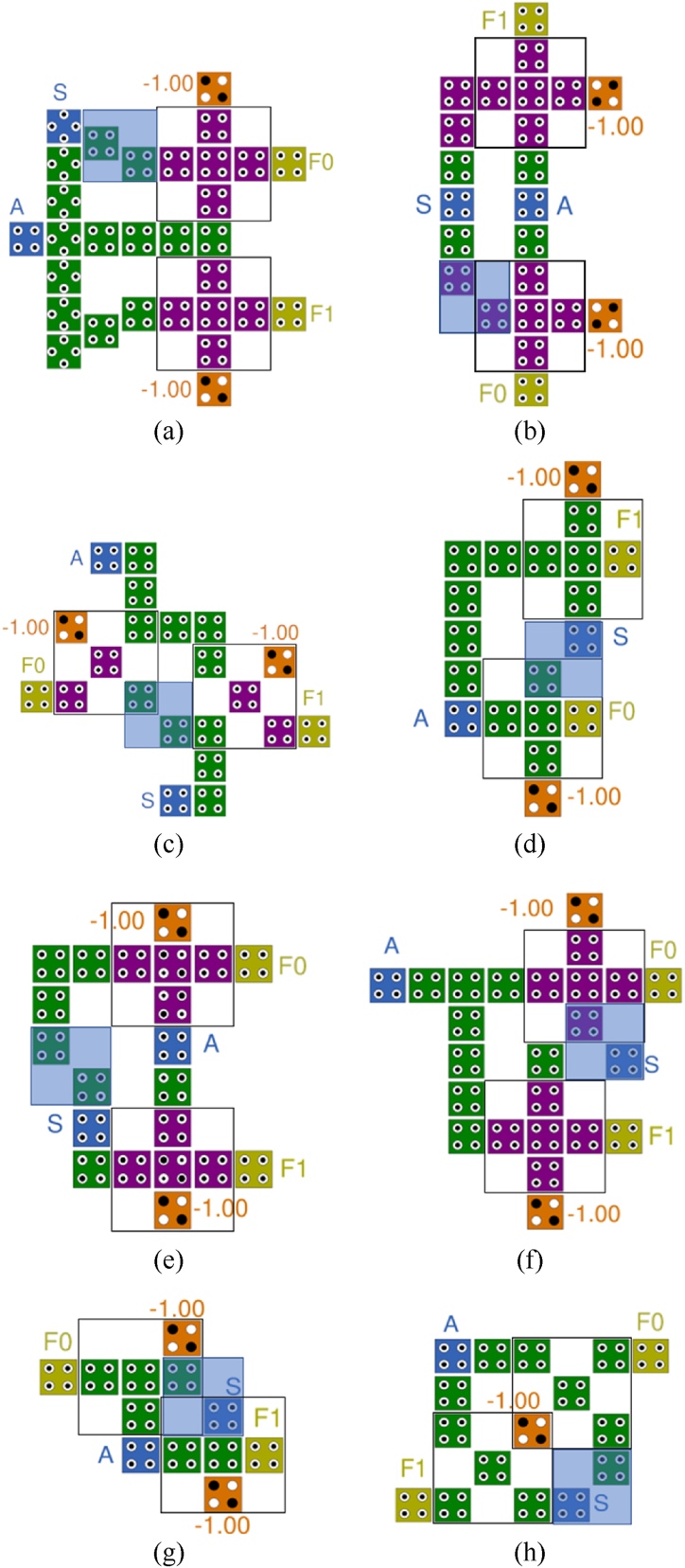
A 1-to-2 DeMux is a combinational circuit in which one input A is distributed to two output lines F0 or F1 by a selection input S [14,15]. To implement the two outputs F0 = AS′ and F1 = AS using QCA, they can be implemented using two majority gates and one inverter, respectively [16,17]. Fig. 4 introduces the most recent and excellent 1-to-2 DeMux research [[14], [15], [16], [17], [18], [19], [20], [21]]. In Fig. 4, the part marked with an empty 3✕3 square corresponds to the majority gate, and the portion marked with a 2✕2 light blue square represents the inverter.
Fig. 4.
Existing 1-to-2 demultiplexers: (a) J. Iqbal et al. [14]; (b) A. Mallaia et al. [15]; (c) F. Ahmad [16]; (d) V. K. Sharma et al. [17]; (e) S. Afrooz et al. [18]; (f) A. Khan et al. [19]; (g) V. K. Sharma [20]; (h) R. Akbari-Hasanjani et al. [21].
Fig. 4(a) shows input and crossover using a 45° rotated cell. The input S uses a weak inverter to pass the value of S′ to the first majority gate on the right. In the lower part, the weak inverter is used again, but this time, it plays the role of changing the value of S′ to S. At this time, the input value A passes through the 45° rotated cell and provides input values to both AND gates. The overall symmetrical structure can be seen as having high modularity, but the overall use of space is high due to the coplanar crossover structure [14].
In Fig. 4(b), two inputs S and A are placed between two majority gates so that operations can proceed simultaneously on both sides. Additionally, S′ is produced using a weak inverter for the output of F0 [15]. Unlike Fig. 4(a), where the inputs are on the left and the outputs are on the right, the inputs in Fig. 4(b) are gathered in the center, which has the disadvantage that a crossover is required to expand the circuit.
Fig. 4(c) shows two AND gates constructed using a rotated majority gate. It is structured in a radial form with two inputs coming in from the top and bottom and two outputs going out to the left and right [16]. Fig. 4(d) uses the same two majority gates and one inverter as the existing structures, but is the first structure to derive the result using only one clock phase [17].
Fig. 4(e) is designed similarly to existing structures and has no special structural parts [18], and Fig. 4(f) inverts the input value S once, uses S′ as the input of one majority gate, and uses the inverted value as the input of one majority gate. It has the characteristic of being reversed once again and using S as an input to the other majority gate [19].
Fig. 4(g) has a slightly special structure. The F1 output uses the majority gate of the same structure as before, but the AND gate for the F0 output is designed based on cell interaction by Coulomb repulsion. This uses the fewest cells and can produce the desired results in a small space [20]. Fig. 4(h) uses two rotated majority gates and shares a fixed cell to minimize space and show high space utilization [21]. Fig. 4(g) and (h) are designed to overlap the space of the majority gate as much as possible to minimize space, and have the common advantage of using a single clock phase, but the two input lines are separated between the two outputs. The disadvantage is that a crossover type connection line is required for expansion. The most recently developed DeMux in Ref. [22] was excluded from the review because it uses four clock phases for delay.
2.3. Review of 1-to-4 demultiplexers
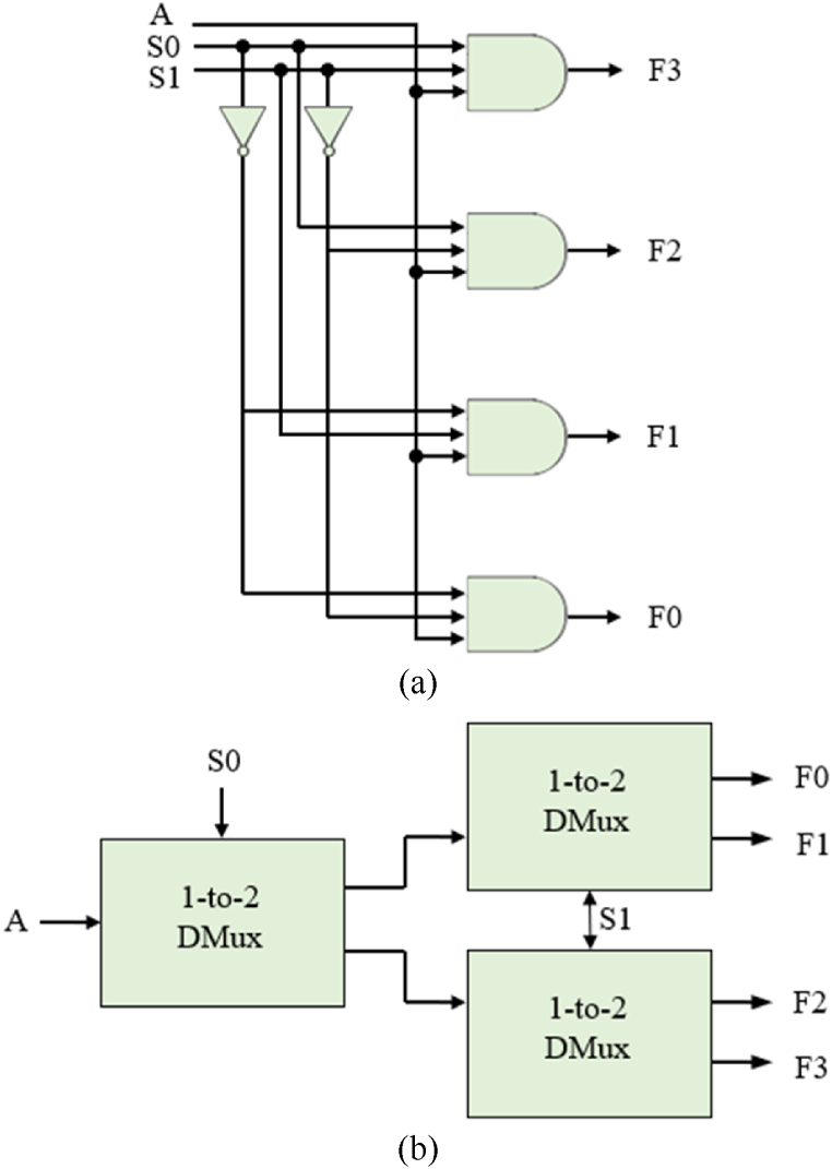
There are two main ways to extend 1-to-2 DeMux to 1-to-4 DeMux. One is to use four 3-input AND gates and two inverters as shown in Fig. 5(a), and the other is to use three 1-to-2 DeMuxes as shown in Fig. 5(b).
Fig. 5.
Logic diagrams of 1-to-4 demultiplexer: (a) four 3-input AND gated based DeMux; (b) three 1-to-2 DeMux based DeMux.
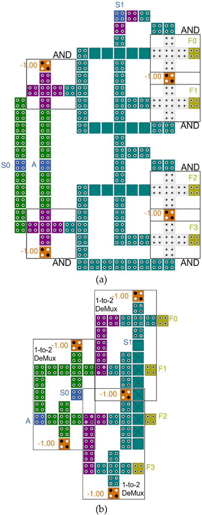
Iqbal et al. used coplanar crossovers using 45° rotated cells and translated cells, and implemented 1-to-4 DeMux using 8 AND gates [14]. Ahmad et al. proposed an efficient 3-input AND gate using a 4-input majority gate and implemented 1-to-4 DeMux using coplanar crossovers using clock phase [16]. Afrooz et al. used three DeMuxes and used coplanar crossovers using 45° rotated cells and translated cells [18].
Fig. 6(a) shows the 1-to-4 DeMux proposed by Safoev et al. This structure shares the fixed cell of the AND gates and uses multi-layer crossovers to increase area efficiency [23]. Sharma et al. implemented 1-to-4 DeMux by connecting three 1-to-2 DeMux as shown in Fig. 6(b). At this time, multi-layer crossover was used to allow the second and third DeMux to share second selector, S1 [17].
Fig. 6.
Existing multi-layer 1-to-4 demultiplexers: (a) Safoev et al. [23]; (b) Sharma et al. [17].
3. Proposed demultiplexer
In this section, we propose a 1-to-2 DeMux circuit with excellent performance using QCA and show the operating principle of the circuit through physical proof of the operation designed by cell interaction.
3.1. Proposed 1-to-2 DeMux
By reviewing existing studies, we identify various problems and specify the following five design improvement issues to design a structure that is superior to the existing best circuits.
-
1)
Since the minimum delay must be used, the result must be derived in only one clock phase.
-
2)
To minimize the area, two operation gates must be designed to overlap.
-
3)
To expand the circuit, design the two output lines in the same direction.
-
4)
Circuit design based on cell interaction is necessary to increase area utilization.
-
5)
To reduce the energy dissipation, the number and density of cells must be minimized.
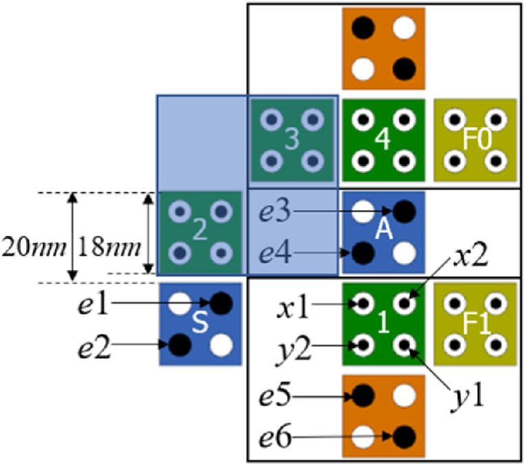
The proposed structure is shown in Fig. 7 in a coplanar format in which both majority gate and cell interaction are applied. We design an efficient QCA-based circuit that solves various existing problems and takes various design costs into consideration. The input value A is located in the center of the circuit to be commonly used in two AND operations. The value of S′ is input to the upper AND gate through a weak inverter, and the value of F0 = S′A is output. The AND operation used at the bottom of the circuit is designed based on cell interaction. It is possible to take the form of a majority gate by placing a cell between input cell S and Cell #1, but there is a problem that energy dissipation also increases as the cell density increases. Also, even if there is no corresponding cell, the Coulomb reaction force for the value of S cell can be sufficiently transmitted to Cell #1, so the value of F1 = SA is still output. The Coulomb repulsion of Cell #1 is physically proven in the next section.
Fig. 7.
Proposed coplanar QCA based 1-to-2 DeMux.
3.2. Physical proof
Unlike circuits defined by majority gates and logically constructed, operations constructed by cell interactions must prove the operation of the circuit using the physical values of electrons generated by Coulomb repulsion. For physical proof, the following QCA parameters and assumptions about the surrounding environment are required.
-
1)
Cell size: 18 nm ✕ 18 nm.
-
2)
Intercell distance: 2 nm.
-
3)
Radius of effect: 65 nm.
-
4)
Location of four quantum dots: each corner of a square cell.
In the proposed DeMux, operations by cell interaction must confirm that Cell #1 in Fig. 4 performs AND gate operations by surrounding cells. For physical proof, when the polarization of Cell #1 is −1 or +1, the positions of the electrons are (x1, y1) or (x2, y2), respectively, as shown in Fig. 7. The cells that can affect Cell #1 are S, A, and fixed cells, and each electron is denoted as e1 to e6. Equation (1) represents the potential energy between two electrons, and . is potential energy, is Coulomb's constant, and represent the amount of electric charge, and represents the distance between two electrons.
Therefore can be expressed in C and has the same constant value as equation (2). The sum of potential energies is calculated as equation (3) [24,25].
| (1) |
| (2) |
| (3) |
when the polarization of Cell #1 is −1, let's assume that there is an electron at the position (x1, y1) and find the sum of the potential energies of the surrounding electrons. First, the potential energies of x1 on Cell #1 and e1 to e6 are respectively as follows.
The sum of the potential energies of x1 and the six electrons from e1 to e6 is equal to equation (4).
| (4) |
Additionally, the potential energies of y1 and e1 to e6 of Cell #1 are respectively as follows.
The sum of the potential energies of the 6 electrons of y1 and e1 to e6 is equal to equation (5).
| (5) |
thus, when the polarization of Cell #1 is −1, the sum of the potential energies of the surrounding electrons is equal to equation (6).
| (6) |
Using the same method as mentioned above, when the polarization of Cell #1 is + 1, let's assume that there is an electron at the position (x2, y2) and find the sum of the potential energies. First, the potential energy of x2 of Cell #1 and e1 to e6 are respectively as follows.
The sum of the potential energies of x2 and the six electrons from e1 to e6 is equal to equation (7).
| (7) |
Additionally, the potential energies of y2 and e1 to e6 of Cell #1 are respectively as follows.
The sum of the potential energies of the 6 electrons of y2 and e1 to e6 is equal to equation (8).
| (8) |
thus, when the polarization of Cell #1 is + 1, the sum of the potential energies of the surrounding electrons is equal to equation (9).
| (9) |
As shown in equations (6) and (9), the value of is low, resulting in the conclusion that it is correct for Cell #1 to be located at x2 and y2. Therefore, in the situation shown in Fig. 6, Cell #1 has P = +1.
3.3. Proposed 1-to-4 DeMux
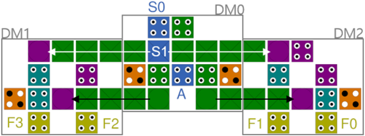
Fig. 8 shows a multi-layered 1-to-4 DeMux constructed using the three proposed 1-to-2 DeMuxes. The expansion of the coplanar method has a very large impact on the performance indicators depending on the location of the input and output cells of the unit DeMux, so it is difficult to calculate the design cost of the expanded structure. Therefore, using a multi-layer crossover, the same level of expansion can be applied to all circuits regardless of the location of the input/output cells of the unit DeMux, and it can be easily expanded to bigger circuits using the same method.
Fig. 8.
Circuit expansion to 1-to-4 DeMux using three proposed 1-to-2 DeMuxes with multi-layer crossover.
At the first clock phase, the input data, A and the selection input, S0, are input to the first demultiplexer, DM0. The values output at the same clock phase are transmitted to the 3rd layer and transmitted as black arrows to be input as data of DM1 and DM2. At the same time, the second selection input, S1, is input from layer 3 and is transmitted to DM1 and DM2 as shown by the white arrow. At the second clock phase, all values in layer 3 are transmitted to layer 1 as input values of DM1 and DM2, and simple inverter is performed on selected input values. At the third and final clock phase, all AND gates are performed simultaneously and the results are output from F0 to F3.
Table 1 shows the truth Table 1, Table 2, Table 3, Table 4 DeMux. When the input data, A, is 0, all result values are output as 0 regardless of the selected input value. When input data A is 1, one 1 is output to each of the four output terminals from F0 to F3 according to the two selected input values, S0 and S1.
Table 1.
Truth table of 1-to-4 DeMux.
| Input |
Output |
|||||
|---|---|---|---|---|---|---|
| A | S0 | S1 | F0 | F1 | F2 | F3 |
| 0 | 0 | 0 | 0 | 0 | 0 | 0 |
| 0 | 0 | 1 | 0 | 0 | 0 | 0 |
| 0 | 1 | 0 | 0 | 0 | 0 | 0 |
| 0 | 1 | 1 | 0 | 0 | 0 | 0 |
| 1 | 0 | 0 | 1 | 0 | 0 | 0 |
| 1 | 0 | 1 | 0 | 1 | 0 | 0 |
| 1 | 1 | 0 | 0 | 0 | 1 | 0 |
| 1 | 1 | 1 | 0 | 0 | 0 | 1 |
Table 2.
Performance comparison and CostAD of 1-to-2 DeMux.
| Circuit | Cell |
Area |
Area utilization |
Delay |
CostAD |
|||||
|---|---|---|---|---|---|---|---|---|---|---|
| no. | ratio | nm2 | ratio | proportion | ratio | clocks | ratio | AD2 | ratio | |
| [14] | 30 | 3.00 | 28,124 | 3.68 | 0.42 | 0.83 | 2 | 2.00 | 112,496 | 14.72 |
| [15] | 23 | 2.30 | 21,364 | 2.79 | 0.42 | 0.84 | 2 | 2.00 | 85,456 | 11.18 |
| [16] | 21 | 2.10 | 28,124 | 3.68 | 0.29 | 0.58 | 2 | 2.00 | 112,496 | 14.72 |
| [17] | 19 | 1.90 | 17,444 | 2.28 | 0.42 | 0.84 | 1 | 1.00 | 17,444 | 2.28 |
| [18] | 21 | 2.10 | 18,644 | 2.44 | 0.44 | 0.88 | 2 | 2.00 | 74,576 | 9.76 |
| [19] | 24 | 2.40 | 28,124 | 3.68 | 0.33 | 0.67 | 2 | 2.00 | 112,496 | 14.72 |
| [20] | 12 | 1.20 | 11,564 | 1.51 | 0.40 | 0.80 | 1 | 1.00 | 11,564 | 1.51 |
| [21] | 16 | 1.60 | 13,524 | 1.77 | 0.46 | 0.91 | 1 | 1.00 | 13,524 | 1.77 |
| [22] | 23 | 2.30 | 24,564 | 3.21 | 0.37 | 0.73 | 4 | 4.00 | 393,024 | 51.42 |
| Fig. 6 | 10 | 1.00 | 7644 | 1.00 | 0.50 | 1.00 | 1 | 1.00 | 7644 | 1.00 |
Table 3.
Energy dissipation and CostED of 1-to-2 DeMux.
| Circuit | Avg_Ebath |
Error_Avg |
Sum_Ebath |
Error_Sum |
CostED |
|||||
|---|---|---|---|---|---|---|---|---|---|---|
| 10−4 eV | ratio | −10−5 eV | ratio | 10−3 eV | ratio | −10−4 eV | ratio | E2D2 | ratio | |
| [14] | 9.33 | 1.16 | 8.30 | 0.97 | 10.30 | 1.17 | 9.13 | 0.97 | 424.36 | 5.47 |
| [15] | 12.00 | 1.50 | 12.10 | 1.41 | 13.20 | 1.50 | 13.30 | 1.41 | 696.96 | 8.98 |
| [16] | 4.50 | 0.56 | 4.04 | 0.47 | 4.95 | 0.56 | 4.44 | 0.47 | 98.01 | 1.26 |
| [17] | 11.10 | 1.39 | 10.80 | 1.26 | 11.80 | 1.34 | 11.90 | 1.26 | 139.24 | 1.79 |
| [18] | 16.50 | 2.06 | 17.80 | 2.07 | 18.10 | 2.05 | 19.60 | 2.08 | 1310.44 | 16.88 |
| [19] | 6.51 | 0.81 | 5.71 | 0.67 | 7.16 | 0.81 | 6.28 | 0.67 | 205.06 | 2.64 |
| [20] | 10.10 | 1.26 | 10.70 | 1.25 | 11.10 | 1.26 | 11.80 | 1.25 | 123.21 | 1.59 |
| [21] | 8.76 | 1.09 | 9.14 | 1.07 | 9.63 | 1.09 | 10.10 | 1.07 | 92.74 | 1.19 |
| [22] | 6.53 | 0.82 | 6.23 | 0.73 | 7.18 | 0.81 | 6.85 | 0.73 | 824.84 | 10.63 |
| Fig. 6 | 8.01 | 1.00 | 8.58 | 1.00 | 8.81 | 1.00 | 9.43 | 1.00 | 77.62 | 1.00 |
Table 4.
Performance and design cost comparison of 1-to-4 DeMux.
| Circuit | Cell |
Areamul. |
Delay |
Sum_Ebath |
CostAD |
CostED |
AOP |
Crossover | ||
|---|---|---|---|---|---|---|---|---|---|---|
| no. | μm2 | clock cycle | 10−2 eV | AD2 | ratio | E2D2 | ratio | 10–1 | ||
| [14] | 198 | 0.2099 | 1.00 | 6.63 | 0.210 | 4.26 | 43.96 | 11.38 | 9.541 | cell rotation |
| [16] | 187 | 0.1439 | 1.75 | 4.06 | 0.441 | 8.94 | 50.48 | 13.07 | 9.521 | clock phase |
| [18] | 90 | 0.1055 | 1.00 | 4.02 | 0.105 | 2.14 | 16.16 | 4.19 | 9.543 | cell rotation |
| [23] | 140 | 0.3749 | 1.00 | 4.77 | 0.375 | 7.61 | 22.75 | 5.89 | 9.545 | multi-layer |
| [17] | 72 | 0.1818 | 0.75 | 2.76 | 0.102 | 2.07 | 4.28 | 1.11 | 9.546 | multi-layer |
| Fig. 8 | 64 | 0.0876 | 0.75 | 2.62 | 0.049 | 1.00 | 3.86 | 1.00 | 9.555 | multi-layer |
4. Comparison and simulation
The simulation of the circuit was performed using QCADesigner 2.0.3, using the “Bistable Approximation” engine [26,27], and the values of the parameters are as follows. number of samples; 12,800, convergence tolerance; 0.001, radius of effect; 65 nm, relative permittivity; 12.9, clock high; 9.8 × 10⁻²² J, clock low; 3.8 × 10⁻²³ J, clock shift; 0, clock amplitude factor; 2.0, cell size; 18 nm, dot diameter; 5 nm, cell separation; 2 nm, layer separation; 11.5 nm, maximum iterations per sample; 100 and randomize simulation order.
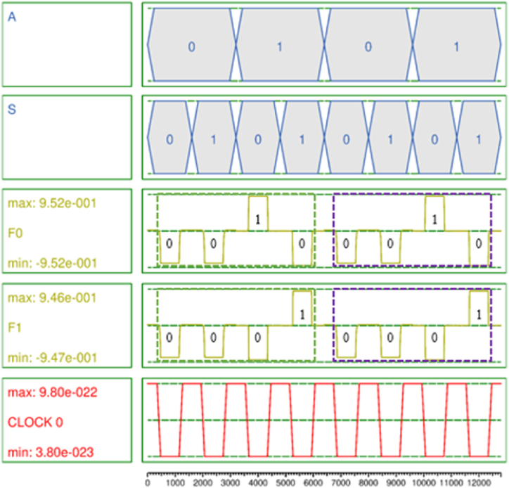
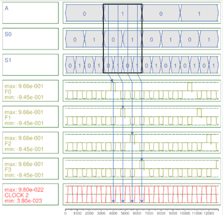
Fig. 9 shows the simulation result of the proposed 1-to-2 DeMux, and it was confirmed that the output was very stable without any signal noises. The green dotted rectangle and the purple dotted rectangle show that F0 and F1 are outputting accurate results in the first and second clock cycles. Fig. 10 shows the simulation results of the proposed 1-to-4 DeMux. As shown in Tables 1 and it operates only when the input data A is 1, and 1 is output at clock 2 in order from F0 to F3 according to the permutation of S0 and S1 values.
Fig. 9.
Simulation result of the proposed 1-to-2 DeMux.
Fig. 10.
Simulation result of the proposed 1-to-4 DeMux.
A variety of factors can be used to determine the performance of a circuit. The number of cells is the most basic element that makes up a circuit and is one of the important factors that can determine the size of the entire circuit. Area represents the two-dimensional rectangular space needed to construct a circuit. However, the area of the multi-layer structure is calculated as equation (10) considering the design complexity.
| (10) |
where m is the number of layers on a multi-layer structure to reflect the higher area cost of a multi-layer design over a coplanar structure [28,29].
In addition, the ratio of space used by actual cells in the corresponding rectangle is displayed as Area utilization. Delay indicates the clock phase required until the first output appears. Among various methods for calculating design costs, the most commonly used method for circuit analysis is to multiply the space required for circuit design by the delay. As the importance of delay has increased with recent hardware developments, equation (11) is often used [28,30].
| (11) |
where A and D refer to the area required for circuit design and the delay required for output, respectively. In this study, considering the importance of D, it is calculated by setting l = 2.
Table 2 shows a comparison of the proposed DeMux with excellent circuits that have been studied recently. The table shows the performance of each field and the ratio of existing circuits when the proposed structure is set to 1. The proposed structure produces results with only 10 cells and only 1 clock phase in a space of 7644 nm2. Among recent studies, the circuit in Ref. [20] proposed in 2023 shows the best results, but it was confirmed that it uses relatively 20 % more cells and requires 51 % more area than the proposed study. Area utilization was the highest at 46 % among existing studies in the circuit proposed by R. Akbari-Hasanjani et al., in 2023 [21], but the proposed study was found to be the best, achieving 50 %. At last, the proposed circuit produced the best results in .
To measure the energy dissipation of a QCA circuit, calculation of a quantum mechanism using a Hamiltonian matrix is required [31,32]. In the proposed study, energy dissipation was measured using QCADesigner-E, “coherence vector with energy” was used as the simulation engine [33], and the related parameters and environment settings were as follows. Temperature; 1 K, relaxation time; 1.0 × 10⁻¹⁵s, clock/input period; 4.0 × 10⁻¹²s, time step; 1.0 × 10⁻¹⁶s, clock high; 9.8 × 10⁻²²J, clock low; 3.8 × 10⁻²³J, clock shift; 0, clock slope; 1.0 × 10⁻¹²s, relative permittivity: 12.9.
Equation (12) is a representative method of measuring the design cost of a QCA circuit including energy dissipation.
| (12) |
where and refers to the energy dissipation and the delay of a circuit, respectively, and and m, and n are the weighting factors. Here, a standard energy-delay metric (m = n = 2) has been considered [28].
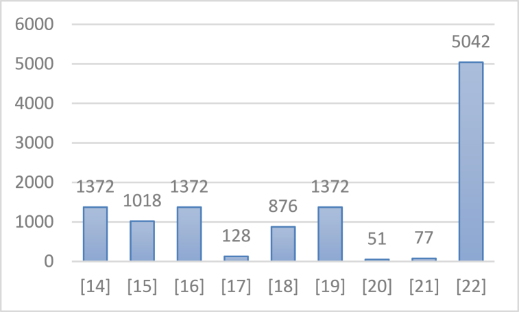
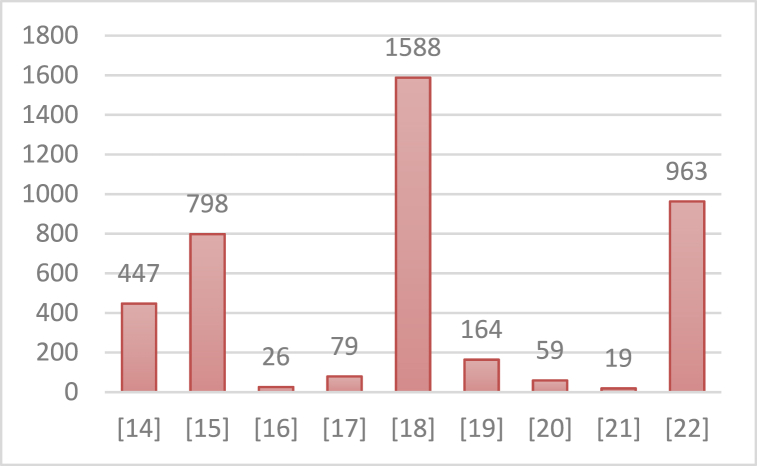
Table 3 shows energy dissipation and associated design costs. The term ‘bath’ refers to the group of quantum cells whose energy dissipation is more in the entire layout environment. Sum_Ebath is the total energy dissipation of Ebath for all the coordinates while Avg_Ebath is the average energy dissipation of Ebath per cycle [34,35]. Circuits with low energy dissipation values typically have low cell density and high latency. However, this may cause a decrease in circuit performance, so the design must carefully consider the trade-offs on both sides. The proposed circuit also has the most efficient results in . Fig. 11, Fig. 12 show how much the proposed circuit is improved in design cost compared to existing circuits. As a result, compared to the best existing studies, the proposed study showed the best results with significant improvement in and , with at least 51 % and 19 %, respectively.
Fig. 11.
Improvement rate of the proposed 1-to-2 DeMux compared to existing studies in .
Fig. 12.
Improvement rate of the proposed 1-to-2 DeMux compared to existing studies in .
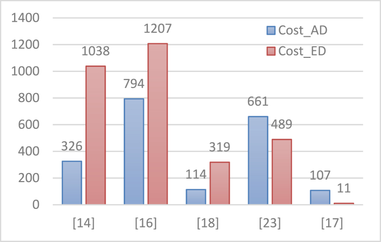
Table 4 compares the performances and design costs of the proposed circuit and existing 1-to-4 DeMux circuits. Areamul. refers to the area where multiple layers are considered as shown in equation (10), Delay is expressed in clock cycle units, Sum_Ebath refers to the total energy dissipation, and AOP refers to the average of output polarization. The proposed 1-to-4 DeMux showed superior performance compared to existing circuits in all performance indicators such as number of cells, area, delay, energy dissipation, and AOP. As shown in Fig. 13, the proposed 1-to-4 DeMux showed significant improvement rates of 107 % and 11 % in and , respectively, compared to the best existing circuit.
Fig. 13.
Improvement rate of the proposed 1-to-4 DeMux compared to existing studies in and .
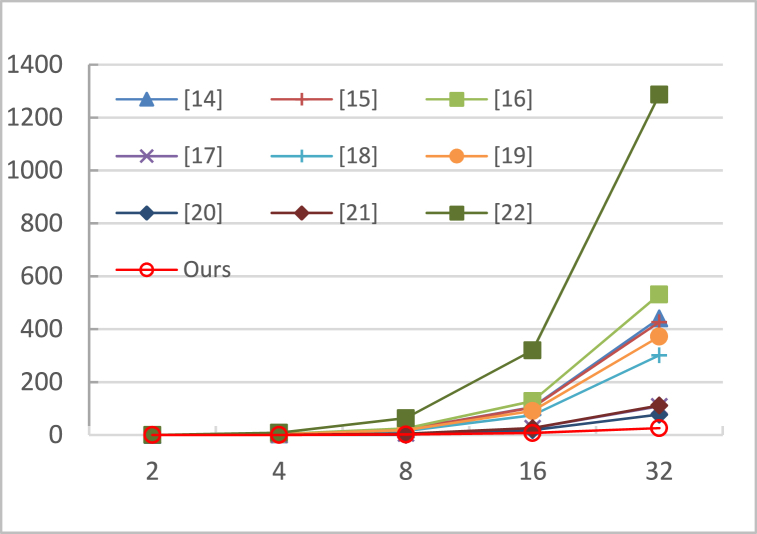
Fig. 14 shows the trend of the value of the circuit according to changes in the output bits of the 1-to-2n DeMux. In order to clearly and fairly expand the circuit, the circuit was expanded using a multi-layer crossover without considering the location of the input/output cells of the unit DeMux. The circuits in Refs. [17,20], and [21] produced a unit DeMux output in a single clock phase like the proposed structure. Therefore, it showed changes similar to the graph of the proposed circuit in proportion to the change in area for each bit. However, for other circuits with large delays, it can be seen that increases significantly as the size of the circuit increases.
Fig. 14.
according to change in size of output-bit of 1-to-2n DeMux (1 ≤ n ≤ 5) (unit: ).
5. Conclusion
Recently, due to the rapid development of communication equipment for data communication and signal routing, the demand for ultra-small and high-speed DeMux circuits at the nano-communication level is intensifying. In this study, we considered a structural design plan that could minimize the area required for circuit design and the delay required to derive the result and optimize energy dissipation. In addition, since the proposed structure was designed using majority gate and cell interaction simultaneously, the structural logic of the proposed circuit was proven through physical verification. The number of cells, area utilization, cell density, and energy dissipation that determine circuit performance are all trade-offs, and finding the optimal value is one of the most important research goals. As a result, the proposed circuits solved most of the problems mentioned above and produced the best results, and this was proven by showing the best results in both design costs.
Funding statement
This work was supported by the Institute of Information and Communications Technology Planning and Evaluation (IITP) Grant by the Korean Government through MSIT (Research on AI-based Cryptanalysis and Security Evaluation) under Grant 2020-0-00126.
Data availability statement
Data included in article/supp. material/referenced in article.
CRediT authorship contribution statement
Jun-Cheol Jeon: Writing – original draft, Visualization, Software, Resources, Methodology, Formal analysis, Data curation, Conceptualization. Changho Seo: Writing – review & editing, Validation, Supervision, Project administration, Investigation, Funding acquisition.
Declaration of competing interest
The authors declare that they have no known competing financial interests or personal relationships that could have appeared to influence the work reported in this paper.
References
- 1.Moore G.E. 2003 IEEE International Solid-State Circuits Conference. Digest of Technical Papers. ISSCC; San Francisco, CA, USA: 2003. No exponential is forever: but "Forever” can be delayed! [semiconductor industry] pp. 20–23. 2003. [Google Scholar]
- 2.Dennard R.H., Gaensslen F.H., Kuhn L., Yu H.N. 1972 International Electron Devices Meeting. 1972. Design of micron MOS switching devices; pp. 168–170. Washington, DC, USA. [Google Scholar]
- 3.Iwai H. Roadmap for 22nm and beyond. Microelectron. Eng. 2009;86(7–9):1520–1528. [Google Scholar]
- 4.Seo D.K., Jeon J.C. QCA-based secure RAM cell structure using logic transformation and cell interaction with signal reliability and energy dissipation in quantum computing. Appl. Sci. 2023;13(18):9998. [Google Scholar]
- 5.Tougaw P.D., Lent C.S. Logical devices implemented using quantum cellular automata. J. Appl. Phys. 1993;75:1818–1825. [Google Scholar]
- 6.Lent C.S., Tougaw P.D., Porod W. Proc. PhysComp '94. 1994. Quantum cellular automata: the physics of computing with arrays of quantum dot molecules; pp. 5–13. Dallas, TX, USA. [Google Scholar]
- 7.Sardinha L.H.B., Costa A.M.M., Neto O.P.V., Vieira L.F.M., Vieira M.A.M. NanoRouter: a quantum-dot cellular automata design. IEEE J. Sel. Area. Commun. 2013;31(12):825–834. [Google Scholar]
- 8.Bahar A.N., Wahid K.A. Design and implementation of approximate DCT architecture in quantum-dot cellular automata. IEEE Trans. Very Large Scale Integr. Syst. 2020;28(12):2530–2539. [Google Scholar]
- 9.Jeon J.C. Multi-layer QCA shift registers and wiring structure for LFSR in stream cipher with low energy dissipation in quantum nanotechnology. Electronics. 2023;12(10):4093. [Google Scholar]
- 10.Safoev N., Jeon J.C. A novel controllable inverter and adder/subtractor in quantum-dot cellular automata using cell interaction based XOR gate. Microelectron. Eng. 2020;222 [Google Scholar]
- 11.Das R., Alam M.D.S., Ahmmed K.T. An energy efficient design of a multi-layered crossover based 3:8 decoder using quantum-dot cellular automata. Heliyon. 2022;8 doi: 10.1016/j.heliyon.2022.e11643. [DOI] [PMC free article] [PubMed] [Google Scholar]
- 12.Jeon J.C., Almatrood A., Kim H.I. Multi-layered QCA content-addressable memory cell using low-power electronic interaction for AI-based data learning and retrieval in quantum computing environment. Sensors. 2023;23:19. doi: 10.3390/s23010019. [DOI] [PMC free article] [PubMed] [Google Scholar]
- 13.Kim H.I., Jeon J.C. Quantum LFSR structure for random number generation using QCA multilayered shift register for cryptographic purposes. Sensors. 2022;22:3541. doi: 10.3390/s22093541. [DOI] [PMC free article] [PubMed] [Google Scholar]
- 14.Iqbal J., Khanday F.A., Shah N.A. IMPACT-2013. 2013. Design of quantum-dot cellular automata (QCA) based modular 2n-1-2n MUX-DEMUX; pp. 189–193. Aligarh, India. [Google Scholar]
- 15.Mallaia A., Swamy G.N., Padmapriya K. Designing efficient multiplexer, demultiplexer QCA logic circuits and power dissipation analysis–A new approach. Int. J. Sci. Eng. Res. 2018;9(7):1995–2004. [Google Scholar]
- 16.Ahmad F. An optimal design of QCA based 2n:1/1:2n multiplexer/demultiplexer and its efficient digital logic realization. Microprocess. Microsyst. 2018;56:64–75. [Google Scholar]
- 17.Sharma V.K. Optimal design for 1: 2n demultiplexer using QCA nanotechnology with energy dissipation analysis. Int. J. Numer. Model. Electron. Netw. Dev. Field. 2021;34 [Google Scholar]
- 18.Afrooz S., Navimipour N.J. An effective nano design of demultiplexer architecture based on coplanar quantum-dot cellular automata. IET Circuits, Devices Syst. 2021;15:168–174. [Google Scholar]
- 19.Khan A., Arya R. Towards the design and analysis of multiplexer/demultiplexer using quantum dot cellular automata for nano systems. J. New Mater. Electrochem. Syst. 2022;25:62–71. [Google Scholar]
- 20.Sharma V.K. QCA-based reliable fundamental units for multiplexer-demultiplexer and D-flip-flop. Int. J. Nanosci. 2023;22 [Google Scholar]
- 21.Akbari-Hasanjani R., Sabbaghi-Nadooshan R. Tree router design using a novel optimal QCA DEMUX. Nano Commun. Netw. 2023;35 [Google Scholar]
- 22.Vahabi M., Rahimi E., Lyakhov P., Otsuki A. A novel QCA circuit-switched network with power dissipation analysis for nano communication applications. Nano Commun. Netw. 2023;35 [Google Scholar]
- 23.Safoev N., Jeon J.C. Low area complexity demultiplexer based on multilayer quantum-dot cellular automata. Int. J. Control Autom. 2016;9(12):165–178. [Google Scholar]
- 24.Halliday D., Resnick A. seventh ed. John Wiley and Sons, Inc; New York: 2004. Fundamentals of Physics; pp. 3–6. Chaps. [Google Scholar]
- 25.McDermott L.C. Research on conceptual understanding in mechanics,”. Phys. Today. 1984;37(7):24–32. [Google Scholar]
- 26.Walus K., Dysart T.J., Jullien G.A., Budiman R.A. QCADesigner: a rapid design and simulation tool for quantum-dot cellular automata. IEEE Trans. Nanotechnol. 2004;3(1):26–31. [Google Scholar]
- 27.Roshan M.G., Gholami M. Novel level and edge-triggered universal shift registers with low latency in QCA technology. Heliyon. 2024;10 doi: 10.1016/j.heliyon.2024.e26086. [DOI] [PMC free article] [PubMed] [Google Scholar]
- 28.Liu W., Lu L., O'Neill M., Swartzlander E.E. A first step toward cost functions for quantum-dot cellular automata designs. IEEE Trans. Nanotechnol. 2014;13(3):476–487. [Google Scholar]
- 29.Chu Z., Li Z., Xia Y., Wang L., Liu W. BCD adder designs based on three-input XOR and majority gates. IEEE Trans. Circ. Syst. II Express Briefs. 2021;68(6):1942–1946. [Google Scholar]
- 30.Mead C., Rem M. Cost and performance of VLSI computing structures. IEEE Trans. Electron. Dev. 1979;26(4):533–540. 1979. [Google Scholar]
- 31.Srivastava S., Sarkar S., Bhanja S. “Estimation of upper bound of power dissipation in QCA circuits. IEEE Trans. Nanotechnol. 2009;8(1):116–127. [Google Scholar]
- 32.Kim H.I., Jeon J.C. Non-restoring array divider using optimized CAS cells based on quantum-dot cellular automata with minimized latency and power dissipation for quantum computing. Nanomaterials. 2022;12:540. doi: 10.3390/nano12030540. [DOI] [PMC free article] [PubMed] [Google Scholar]
- 33.QCADesigner-E. Available online: https://github.com/FSillT/QCADesigner-E (accessed on 20 April. 2024).
- 34.Timler J., Lent C.S. Power gain and dissipation in quantum-dot cellular automata. J. Appl. Phys. 2002;91:823–831. [Google Scholar]
- 35.Sill Torres F., Wille R., Niemann P., Drechsler R. An energy-aware model for the logic synthesis of quantum-dot cellular automata. IEEE Trans. Comput. Aided Des. Integrated Circ. Syst. 2018;37(12):3031–3041. [Google Scholar]
Associated Data
This section collects any data citations, data availability statements, or supplementary materials included in this article.
Data Availability Statement
Data included in article/supp. material/referenced in article.


