

Abstract
Optical encoders are widely used circuits in digital systems. One of the most critical features of an optical encoder is the power values in two logic states; low and high. The difference between these two values is expressed with the contrast ratio (CR) parameter. This research has designed and simulated an optical encoder based on a two-dimensional (2D) photonic crystal with four inputs and two outputs. The results show that the proposed structure has low power in low mode and high intensity in high mode. This difference in two logical modes has caused the proposed encoder to have CR = 19.8 dB, which is improved compared to previous works. Also, the proposed structure is very compact and its footprint is as small as 96.88 µm2. The data speed for the designed encoder is . This encoder can be used in high-speed optical integrated circuits with low error according to the obtained values.
Keywords: Optical encoder, Photonic crystals, Photonic bandgap, Optical integrated circuits
Subject terms: Engineering, Optics and photonics, Physics
Introduction
So far, various electronic circuits have been designed based on transistors, in which electrons are used as charge carriers. In other words, the transistor is used as the building block of the encoder. With the increase in information and the need for very high-speed processors, designing digital circuits based on optical structures is necessary. One of the suitable structures for designing all kinds of digital circuits is photonic crystals1–6.
Photonic crystals are alternating structures of insulating or dielectric materials that reflect a range of light wavelengths. These structures alternate in one, two, or three dimensions7–12. Two-dimensional photonic crystals have more applications than other types. Two-dimensional photonic crystals can be created by placing dielectric rods regularly in two dimensions. When light shines in an alternating direction, some wavelengths of light cannot enter the structure and are reflected. To use photonic crystals as optical waveguides, the wavelength of light sources should be in the range of photonic bandgap (PBG)13–16.
The property of PBG is used to design many logic circuits, which can be referred to as all types of logic gates. So far, many circuits have been reported for designing optical logic gates such as NOT, OR, AND, XOR, and XNOR17–24.
Also, combined circuits, such as decoder, encoder, multiplexer, adder, and subtractor, have been designed using photonic crystals. Encoders designed optically based on photonic crystals often have a large size or the optical power in low and high modes does not differ much25–32. Some of these encoders have structural complexity and ring resonators are used in them. In this article, an attempt is made to design a structure that has a suitable size and a simple structure that makes it easier to build. Also, attention has been paid to the difference between two logic values, low and high, to increase the contrast ratio (CR) parameter17,33–35.
In this manuscript, first, a basic photonic crystal structure is considered to design the desired optical encoder. Then the band structure analysis was done to determine PBG. According to the band structure results, the appropriate wavelength will be determined for the sources. In selecting the structure, it has been tried that the wavelength of optical fiber communication can be used in it. Then the waveguide paths are created to transmit light from the inputs to the output so that the light is transmitted from 4 inputs to 2 outputs based on the function of the encoder. The number of defective rods is considered a variable to optimize the desired structure, and by changing them, the best outputs are obtained.
Optical encoder based on photonic crystals
Digital encoders are circuits that take input data and produce its equivalent binary code in the output. According to the truth table of the decoder, at any time, only one of the entries can be in the logical state “1”. The truth table of the 4-to-2 encoder is listed in Table 1.
Table 1.
The truth table of 4-to-2 encoder.
| Inputs | Outputs | ||||
|---|---|---|---|---|---|
| X | Y | ||||
| 1 | 0 | 0 | 0 | 0 | 0 |
| 0 | 1 | 0 | 0 | 1 | 0 |
| 0 | 0 | 1 | 0 | 0 | 1 |
| 0 | 0 | 0 | 1 | 1 | 1 |
First, the location of the input and output sources and the path of the waveguides must be determined to design the desired encoder. Figure 1 shows the schematic of the proposed structure to reach the desired encoder. The figure shows that the encoder has four inputs, , and and two outputs, X and Y.a
Fig. 1.
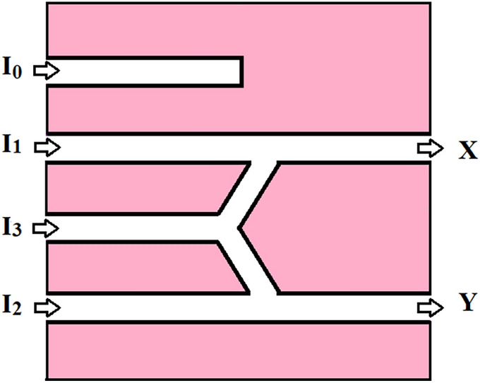
Schematic of the proposed structure for the optical encoder.
To create the final optical encoder circuit, a two-dimensional photonic crystal structure, including silicon rods in air, is selected. The selected lattice for this structure is hexagonal, which includes 17 rods in the X-direction and 19 rods in the Z-direction. The lattice constant for this structure is equal to 0.58 μm, and the radius of the rods is equal to 0.116 μm. Therefore, the footprint of the proposed structure is as small as 96.88 µm2. The band structure calculations have been used to investigate the behavior of light in this structure. These calculations were obtained using the plane wave expansion (PWE) method. The band structure results are shown in Fig. 2.
Fig. 2.
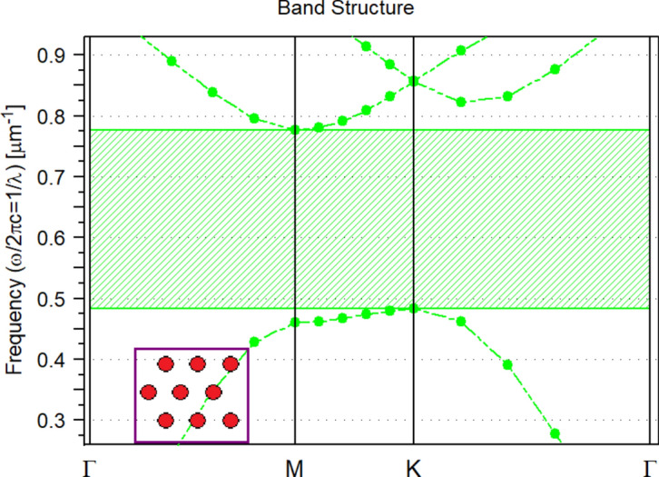
The band structure calculations and photonic band gap.
Results and discussions
Figure 2 shows that a photonic band gap has been created in the range of λ = 1.28–2.08 µm. In this design, the wavelength used for light sources is 1.55 μm, which is used in fiber optic telecommunications. In the next step, the inputs and outputs are determined by creating line and point defects in the photonic crystal, and the waveguide paths are selected to connect the inputs and outputs. Figure 3 shows the designed encoder and the paths of inputs and outputs. As seen in Fig. 3, the inputs are on the left side, and the outputs are on the right side of the structure.
Fig. 3.
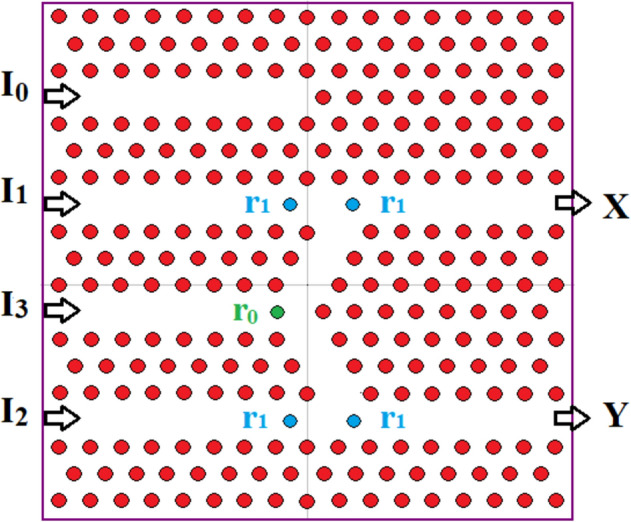
The final structure for the optical encoder.
In the path of inputs and , two rods with radius are placed as defect rods, which can be changed to obtain optimal results in the output. Also, in the input path , a defect rod with radius is considered a defect rod.
To optimize the outputs (decrease power in logical 0 mode and increase optical power in logical 1 mode), defect rods and are considered variable parameters, and by changing them, the output powers are obtained in two logical modes. To optimize the outputs, the defect rods and are considered as variables, and by changing them, the output powers are obtained in two logical states. Considering that the input has no connection with the outputs, the amount of power in the outputs does not have much dependence on this input. Therefore, the optimization has been done for the other three inputs.
In the first case where , the optical power at the X and Y outputs has been calculated for different values of and . The diagram of these changes is shown in Fig. 4. In this case, the outputs should be X = 1 and Y = 0. Therefore, it should be seen that the highest power for the X output and the lowest power for the Y output occur for what values of and
Fig. 4.

Output optical power for for some values of with respect to in (a) X output and (b) Y output.
Figure 4a shows that high power values for X and low power values for Y occur simultaneously in the range of and in the range of . The optical power at the Y output is also shown in Fig. 4b. According to this figure, it can be seen that in the same range where the output of X is acceptable, the output of Y also has a suitable response.
According to the symmetry of two inputs and , the same analysis is also true for the outputs in the case of , and the high-power values for Y and low power values for X will have a diagram similar to Fig. 4. Of course, in this case, X output should have the lowest value and Y output should have the highest value. This situation occurs in the range and in the range . Then the outputs are checked and calculated for state . In this case, the optical power at the outputs has been calculated for different values of and . Figure 5 shows the diagram of these changes.
Fig. 5.

Output optical power for in (a) X output and (b) Y output.
Considering that in this case, both outputs are expected to be in logic 1 state, the optical power in both outputs should be high. Figure 5 shows that for a number of radii and the optical power is high. According to both graphs of Figs. 4 and 5, it can be seen that the best condition for the encoder to have the best response occurs in the radii of and . According to the results, the simulation has been done for this state, and the optical power diagram in the outputs has been calculated. Figures 6, 7, 8, 9 show these diagrams.
Fig. 6.

Output optical power for .
Fig. 7.
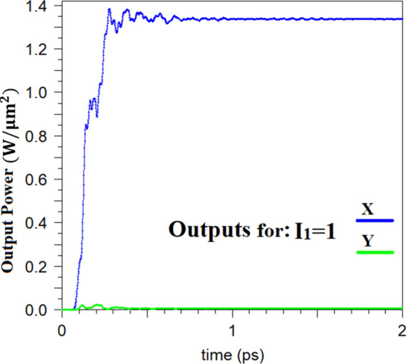
Output optical power for .
Fig. 8.
Output optical power for .
Fig. 9.
Output optical power for .
Figure 6 shows the output power when the input is . The obtained figure shows that in this case both outputs have very little light power and can be considered as logic 0. The power measured in the outputs in this case is W/µm2 in the X output and 0 in the Y output.
Figure 7 shows the optical power diagram in the outputs when the input . In this case, the output in X is equal to W/µm2, and in the output, Y is equal to 0.00. These outputs mean that X can be considered as logic 1 and Y as logic 0.
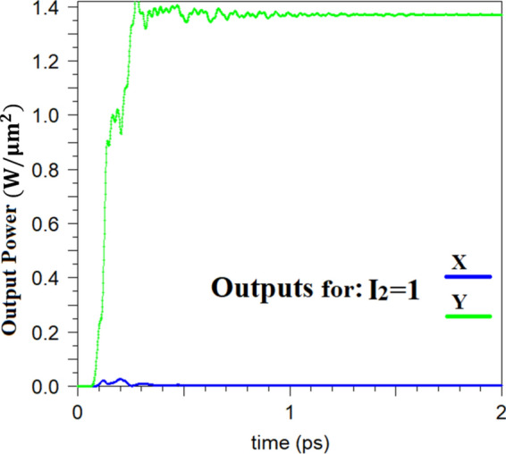
In the next case where the input is , the output power is also measured and its diagram is shown in Fig. 8. In this case, the situation is the opposite of the previous one, that is, X output must have low power and Y output must have high power. According to Fig. 8, which confirms this situation, it can be shown that the optical power at X output is equal to 0 and the power at Y output is equal to W/µm2. In other words, the X output has a logical 0 state and the Y output has a logical 1 state.
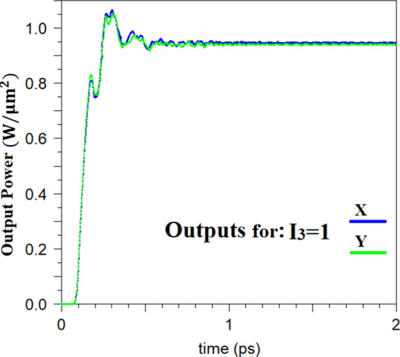
In the last case, where the input is , the power is calculated in terms of time in the outputs and the results of these calculations are shown in Fig. 9. In this case, both outputs have high power, which was expected. The power measured in both outputs is the same for this mode, and their value is equal to W/µm2. It can be said that this power is equivalent to logic 1 in both X and Y outputs.
For the designed encoder, the CR parameter is defined as14:
| 1 |
According to this relationship, the lowest value of power is considered to be logical 1, and the highest value is logical 0. With this definition, the CR value obtained for the designed encoder will be 19.8 dB. A high value of CR indicates a high power difference in two logic states, high and low.
This increase in the value of CR reduces the error in detecting logical values 0 and 1 in the outputs. Figure 10 can be used to show how the power is distributed in the waveguide paths after reaching stability. Figure 10 shows how the optical power is distributed in the waveguide paths for different input modes. This figure also shows the status of high or low powers in the outputs, which is consistent with the previous results.
Fig. 10.

Output optical power distribution for (a) , (b) , (c) , and (d) .
To calculate the data transmission speed or bit rate (BR), an optical pulse is given to the input, in which case both outputs are set to 1. The width of this pulse should be enough for the outputs to be in a stable state. Then, the pulse is interrupted, and the output graph is obtained. Figure 11 shows the output response diagram to the input pulse.
Fig. 11.

The response of the outputs to the input pulse.
Figure 11 shows that the total time for the outputs to reach a stable state at the maximum point after applying the pulse and to reach zero after the pulse is stopped is 0.5 ps. Therefore, the bit transfer speed can be obtained as . The obtained BR value is good for the proposed encoder, and this optical encoder is suitable for high-speed integrated circuits. The reason for the high speed of the proposed encoder is its small size and the use of simple waveguides and short paths. Table 2 compares the important parameters of the proposed encoder with those of the 4-to-2 encoders presented in other works.
Table 2.
Comparison between the proposed encoder and other works.
The proposed structure has a longer delay time than some previous works, but this difference is not very big. In this design, the size of the proposed structure is reduced by about 26% compared to the best work in Table 230. Also, the value of CR indicates the high difference between the two power values in high and low logical states, which reduces the detection error in the output.
Figure 12 shows the output spectrum for different input modes. In this figure, the output power is shown in terms of wavelength. As can be seen in the figure, the structure's best performance is at the wavelength, which is used in today's optical fiber communications. The encoder responds correctly at wavelengths around ; that is, with wavelength changes around the main wavelength, this structure still works correctly.
Fig. 12.

The output spectrum of the output ports.
Conclusions
This paper used photonic crystals to design an optical encoder with a small size and high CR. One of the characteristics of this structure was that the waveguide paths were simple, and few simple defects were used, which makes it suitable for design and construction. The power of the light source in the “off” state was used to define logic 0, and the source in the “on” state was used to define logic 1. The simulation results showed that this structure has very low power in logic 0 and high power in logic 1. Increasing the power difference in the 0 and 1 states has increased the CR parameter, which has made the designed circuit have less error for measuring logical values (CR = 19.8 dB). Also, the high speed of the designed encoder () and its footprint (96.88 µm2) were other advantages of this structure.
Acknowledgements
This work was undertaken in the Department of Electrical Engineering, Kermanshah Branch, Islamic Azad University and Nano-photonics and Optoelectronics Research Laboratory (NORLab), Shahid Rajaee Teacher Training University.
Author contributions
G.I.K.C. designed and simulated the structure, F.P. supervised, completed the simulation results, and wrote the manuscript, S.O. verified the structure, edited, and prepared the final draft of the manuscript. All authors have read and agreed to the published version of the manuscript.
Funding
This work was supported by the Shahid Rajaee Teacher Training University under grant number 5973.84.
Data availability
The datasets used and analysed during the current study available from the corresponding author on reasonable request.
Competing interests
The authors declare no competing interests.
Footnotes
Publisher's note
Springer Nature remains neutral with regard to jurisdictional claims in published maps and institutional affiliations.
References
- 1.Pirasteh, A., Roshani, S. & Roshani, S. Compact microstrip lowpass filter with ultrasharp response using a square-loaded modified T-shaped resonator. Turk. J. Electr. Eng. Comput. Sci.26(4), 1736–1746 (2018). 10.3906/elk-1801-127 [DOI] [Google Scholar]
- 2.Roshani, S. & Roshani, S. Design of a very compact and sharp bandpass diplexer with bended lines for GSM and LTE applications. AEU-Int. J. Electron. Commun.1(99), 354–360 (2019). 10.1016/j.aeue.2018.12.014 [DOI] [Google Scholar]
- 3.Hookari, M., Roshani, S. & Roshani, S. Design of a low pass filter using rhombus-shaped resonators with an analytical LC equivalent circuit. Turk. J. Electr. Eng. Comput. Sci.28(2), 865–874 (2020). 10.3906/elk-1905-153 [DOI] [Google Scholar]
- 4.Parandin, F., Moayed, M. & Heidari, F. All-optical diode for terahertz optical power rectification based on two-dimensional photonic crystals. Microelectron. J.136, 105779 (2023). 10.1016/j.mejo.2023.105779 [DOI] [Google Scholar]
- 5.Gangwar, R. K., Pathak, A. K. & Kumar, S. Recent progress in photonic crystal devices and their applications: A review. Photonics10, 1199 (2023). 10.3390/photonics10111199 [DOI] [Google Scholar]
- 6.Vercruysse, D., Sapra, N. V., Yang, K. Y. & Vučković, J. Inverse-designed photonic crystal circuits for optical beam steering. ACS Photon.8(10), 3085–3093 (2021). 10.1021/acsphotonics.1c01119 [DOI] [Google Scholar]
- 7.Farmani, A. Quantum-dot semiconductor optical amplifier: Performance and application for optical logic gates. Majlesi J. Telecommun. Dev.6(3), 93–97 (2017). [Google Scholar]
- 8.Rehman, A. U. et al. Three-dimensional modeling of the optical switch based on guided-mode resonances in photonic crystals. Micromachines14, 1116 (2023). 10.3390/mi14061116 [DOI] [PMC free article] [PubMed] [Google Scholar]
- 9.Chen, C. W. et al. Large three-dimensional photonic crystals based on monocrystalline liquid crystal blue phases. Nat. Commun.8, 727 (2017). 10.1038/s41467-017-00822-y [DOI] [PMC free article] [PubMed] [Google Scholar]
- 10.Tajiri, T. et al. Three-dimensional photonic crystal simultaneously integrating a nanocavity laser and waveguides. Optica6(3), 296–299 (2019). 10.1364/OPTICA.6.000296 [DOI] [Google Scholar]
- 11.Mohammadi, B. et al. Improving the transmission efficiency in eight-channel all optical demultiplexers. Photon Netw. Commun.38, 115–120 (2019). 10.1007/s11107-019-00830-6 [DOI] [Google Scholar]
- 12.Maleki, M. J., Soroosh, M. & Mir, A. Ultra-fast all-optical 2-to-4 decoder based on a photonic crystal structure. Appl. Opt.59, 5422–5428 (2020). 10.1364/AO.392933 [DOI] [Google Scholar]
- 13.Rezaei, M. H., Boroumandi, R., Zarifkar, A. & Farmani, A. Nano-scale multifunctional logic gate based on graphene/hexagonal boron nitride plasmonic waveguides. IET Optoelectron.14(1), 37–43 (2020). 10.1049/iet-opt.2019.0054 [DOI] [Google Scholar]
- 14.Huang, Y., Shi, M., Yu, A. & Xia, L. Design of multifunctional all-optical logic gates based on photonic crystal waveguides. Appl. Opt.62(3), 774–781 (2023). 10.1364/AO.473410 [DOI] [PubMed] [Google Scholar]
- 15.Caballero, L. P., Povinelli, M. L., Ramirez, J. C., Guimarães, P. S. S. & Vilela Neto, O. P. Photonic crystal integrated logic gates and circuits. Opt. Exp.30(2), 1976–1993 (2022). 10.1364/OE.444714 [DOI] [PubMed] [Google Scholar]
- 16.Farmani, A., Mir, A. & Irannejad, M. 2D-FDTD simulation of ultra-compact multifunctional logic gates with nonlinear photonic crystal. J. Opt. Soc. Am. B36(4), 811–818 (2019). 10.1364/JOSAB.36.000811 [DOI] [Google Scholar]
- 17.Parandin, F. & Sheykhian, A. Design and simulation of a 2 × 1 All-Optical multiplexer based on photonic crystals. Opt. Laser Technolo.151, 108021 (2022). 10.1016/j.optlastec.2022.108021 [DOI] [Google Scholar]
- 18.Haddadan, F., Soroosh, M. & Alaei-Sheini, N. Designing an electro-optical encoder based on photonic crystals using the graphene–Al2O3 stacks. Appl. Opt.59, 2179–2185 (2020). 10.1364/AO.386248 [DOI] [PubMed] [Google Scholar]
- 19.Askarian, A., Akbarizadeh, G. & Fartash, M. All-optical half-subtractor based on photonic crystals. Appl. Opt.58, 5931–5935 (2019). 10.1364/AO.58.005931 [DOI] [PubMed] [Google Scholar]
- 20.Askarian, A., Akbarizadeh, G. & Fartash, M. An all-optical half subtractor based on Kerr effect and photonic crystals. Optik207, 164424 (2020). 10.1016/j.ijleo.2020.164424 [DOI] [PubMed] [Google Scholar]
- 21.Askarian, A., Akbarizadeh, G. & Fartash, M. A novel proposal for all optical half-subtractor based on photonic crystals. Opt. Quantum Electron.51(8), 264–272 (2019). 10.1007/s11082-019-1978-6 [DOI] [PubMed] [Google Scholar]
- 22.Seraj, Z., Soroosh, M. & Alaei-Sheini, N. Ultra-compact ultra-fast 1-bit comparator based on a two-dimensional nonlinear photonic crystal structure. Appl. Opt.59, 811–816 (2020). 10.1364/AO.374428 [DOI] [PubMed] [Google Scholar]
- 23.Pavelyev, V., Krivosheeva, Y. & Golovashkin, D. Genetic optimization of the y-shaped photonic crystal NOT logic gate. Photonics10, 1173 (2023). 10.3390/photonics10101173 [DOI] [Google Scholar]
- 24.Naghizade,S., Saghaei, H. A novel design of all-optical half adder using a linear defect in a square lattice rod-based photonic crystal microstructure, arXiv preprint arXiv, 2002.04535, 2020.
- 25.Sani, M. H. et al. An ultrafast all-optical half adder using nonlinear ring resonators in photonic crystal microstructure. Opt. Quant. Electron.52, 107 (2020). 10.1007/s11082-020-2233-x [DOI] [Google Scholar]
- 26.Serajmohammadi, S., Alipour-Banaei, H. & Mehdizadeh, F. Proposal for realizing an all-optical half adder based on photonic crystals. Appl. Opt.57, 1617–1621 (2018). 10.1364/AO.57.001617 [DOI] [PubMed] [Google Scholar]
- 27.Jalali-Azizpoor, M. R., Soroosh, M. & Seifi-Kavian, Y. Application of self-collimated beams in realizing all-optical photonic crystal-based half-adder. Photon. Netw. Commun.36, 344–349 (2018). 10.1007/s11107-018-0786-4 [DOI] [Google Scholar]
- 28.Askarian, A. & Akbarizadeh, G. A novel proposal for all optical 2×4 decoder based on photonic crystal and threshold switching method. Opt. Quant. Electron.54, 84 (2022). 10.1007/s11082-021-03443-4 [DOI] [Google Scholar]
- 29.Serajmohammadi, S., Alipour-Banaei, H. & Mehdizadeh, F. All optical decoder switch based on photonic crystal ring resonators. Opt. Quant. Electron.47, 1109–1115 (2015). 10.1007/s11082-014-9967-2 [DOI] [Google Scholar]
- 30.Mohebzadeh-Bahabady, A. & Olyaee, S. Ultra-fast and compact all-optical encoder based on photonic crystal nano-resonator without using nonlinear materials. Phot. Lett. Pol.11(1), 10–12 (2019). 10.4302/plp.v11i1.890 [DOI] [Google Scholar]
- 31.Naghizade, S., Mohammadi, S. & Khoshsima, H. Design and simulation of an all optical 8 to 3 binary encoder based on optimized photonic crystal OR gates. J. Opt. Commun.42(1), 31–41 (2021). 10.1515/joc-2018-0034 [DOI] [Google Scholar]
- 32.Moniem, T. A. All-optical digital 4 × 2 encoder based on 2D photonic crystal ring resonators. J. Mod. Opt.63(8), 735–741 (2015). 10.1080/09500340.2015.1094580 [DOI] [Google Scholar]
- 33.Mehdizadeh, F., Soroosh, M. & Alipour-Banaei, H. Proposal for 4-to-2 optical encoder based on photonic crystals. IET Optoelectron.11(1), 29–35 (2017). 10.1049/iet-opt.2016.0022 [DOI] [Google Scholar]
- 34.Hassangholizadeh, M., Sabbaghi, R. & Alipour-Banaei, H. A novel all optical reversible 4 × 2 encoder based on photonic crystals. Optik126, 2368–2372 (2015). 10.1016/j.ijleo.2015.05.140 [DOI] [Google Scholar]
- 35.Naghizade, S. & Saghaei, H. A novel design of all-optical 4 to 2 encoder with multiple defects in silica-based photonic crystal fiber. Optik222, 165419 (2020). 10.1016/j.ijleo.2020.165419 [DOI] [Google Scholar]
- 36.Rajasekar, R., Raja, G. T., Jayabarathan, J. K. & Robinson, S. High speed nano-optical encoder using photonic crystal ring resonator. Photon. Netw. Commun.40(1), 31–39 (2020). 10.1007/s11107-020-00891-y [DOI] [Google Scholar]
- 37.Gogga, S., Gowre, S. C. & Sonth, M. V. Design and analysis of 4×2 optical encoder using wave guides and defects mechanism in two dimensional photonic crystals. In 2023 International conference on microwave, optical, and communication engineering (ICMOCE), Bhubaneswar, India, 2023, pp. 1–5.
- 38.Askarian, A. Design and implementation of all optical 4 × 2 encoder based on 2D-PhC platform and optical Kerr effect. Opt. Quant. Electron.55, 822 (2023). 10.1007/s11082-023-04957-9 [DOI] [Google Scholar]
Associated Data
This section collects any data citations, data availability statements, or supplementary materials included in this article.
Data Availability Statement
The datasets used and analysed during the current study available from the corresponding author on reasonable request.