NIST Author Manuscripts logoLink to NIST Author Manuscripts
. Author manuscript; available in PMC: 2024 Sep 19.
Published in final edited form as: Nanotechnology. 2021 Jan 1;32(1):012002. doi: 10.1088/1361-6528/aba70f

Roadmap on Emerging Hardware and Technology for Machine Learning

Karl Berggren 1,*, Qiangfei Xia 2,*, Konstantin K Likharev 3, Dmitri B Strukov 4, Hao Jiang 5, Thomas Mikolajick 6, Damien Querlioz 7, Martin Salinga 8, John R Erickson 9, Shuang Pi 10, Feng Xiong 9, Peng Li 1, Can Li 11, Yu Chen 12, Shisheng Xiong 12, Brian D Hoskins 13, Matthew W Daniels 13, Advait Madhavan 13,14, James A Liddle 13, Jabez J McClelland 13, Yuchao Yang 15, Jennifer Rupp 16, Stephen S Nonnenmann 17, Kwang-Ting Cheng 18, Nanbo Gong 19, Miguel Angel Lastras-Montaño 20, A Alec Talin 21, Alberto Salleo 22, Bhavin J Shastri 23, Thomas Ferriera de Lima 24, Paul Prucnal 24, Alex N Tait 25, Yichen Shen 26, Huaiyu Meng 26, Charles Roques-Carmes 1, Zengguang Cheng 27,28, Harish Bhaskaran 27, Deep Jariwala 29, Han Wang 30, Jeffrey M Shainline 25, Kenneth Segall 31, J Joshua Yang 2, Kaushik Roy 32, Suman Datta 33, Arijit Raychowdhury 34
PMCID: PMC11411818  NIHMSID: NIHMS1670480  PMID: 32679577

Abstract

Recent progress in artificial intelligence is largely attributed to the rapid development of machine learning, especially in the algorithm and neural network models. However, it is the performance of the hardware, in particular the energy efficiency of a computing system that sets the fundamental limit of the capability of machine learning. Data-centric computing requires a revolution in hardware systems, since traditional digital computers based on transistors and the von Neumann architecture were not purposely designed for neuromorphic computing. A hardware platform based on emerging devices and new architecture is the hope for future computing with dramatically improved throughput and energy efficiency. Building such a system, nevertheless, faces a number of challenges, ranging from materials selection, device optimization, circuit fabrication, and system integration, to name a few. The aim of this Roadmap is to present a snapshot of emerging hardware technologies that are potentially beneficial for machine learning, providing the Nanotechnology readers with a perspective of challenges and opportunities in this burgeoning field.

Introduction

It is believed that hardware is on the critical path for the future of artificial intelligence in the big data era [1]. State-of-the-art hardware for machine learning such as the central processing unit (CPU), graphics processing unit (GPU) and tensor processing unit (TPU) are built upon the complementary metal oxide semiconductor (CMOS) transistors. Although superior computing capability has been demonstrated with such hardware, the end of transistor scaling and the separation of logic and memory units in the von Neumann architecture limit the performance in particular energy efficiency, for data-centric tasks. Inspired by the extremely low power consumption of the human brain, neuromorphic hardware has been an intensive research topic, such as those that based on emerging solid state devices.

Emerging non-volatile devices can store information without dissipating power. When organized into a computing system, it can implement a so-called ‘in-memory computing’ (IMC) paradigm, in which computation takes place where the data is stored. IMC avoids the time and energy spent on data shuttling between memory and logic units in a traditional digital computer, especially suitable for tasks in which data needed to be computed are naturally collocated in the physical memory. Taking advantage of physical laws, such as Ohms law for multiplication and Kirchhoff’s current law for summation, IMC with a large-scale emerging device offers massive parallelism as well. Furthermore, the physical computing is analog in nature and the hardware could interface with analog data acquired directly from sensor arrays, reducing the energy overhead from analog/digital conversions. Depending on the properties of the device, such hardware is suitable for three types of applications [2]. Devices with excellent stability can be used to build an inference system where the synaptic weights have already been trained somewhere else. With high enough endurance, they may be incorporated into a training system for scalable algorithms such as backpropagation. For devices with intrinsic dynamic behavior similar to biological synapse and neurons, they may be promising building blocks for spiking neural networks that takes advantage of the timing in electric pulses for computing.

Extensive simulation has shown that neural networks built with emerging non-volatile memories will bring orders of magnitude higher speed-energy efficiencies [3]. However, experimental demonstration of large systems that can solve real-world problems has had limited success to date in part because of the lack of ideal devices that can efficiently implement the machine learning algorithms or faithfully emulate the essential properties of synapses and neurons. In addition, the heterogeneous integration of the devices into massively parallel networks is a major technical obstacle as well.

In the present Roadmap article, we pick up several topics on the emerging neuromorphic hardware and technology with machine learning applications that we think are particularly appealing to the readers of Nanotechnology, a community that is more interested in device and technology rather than machine learning algorithm and neural network architecture. The Roadmap starts with FLASH-based hardware that uses non-volatile transistors and targets inference systems. We believe this is a good segue from CMOS to emerging devices. Several resistance switching phenomena based devices including the phase change, memristor, magnetoresistance and ferroelectric devices are the subject of the next few sections, including the materials selection, electrical property optimization, device fabrication and circuit integration, and metrology control, etc. In addition, new materials (such as 2D materials and organic materials) and technologies (for example, self-assembly) are also covered. Finally, novel concepts, such as using photons, quantum phenomenon, superconductors, and the timing of electrical spikes for computing are introduced.

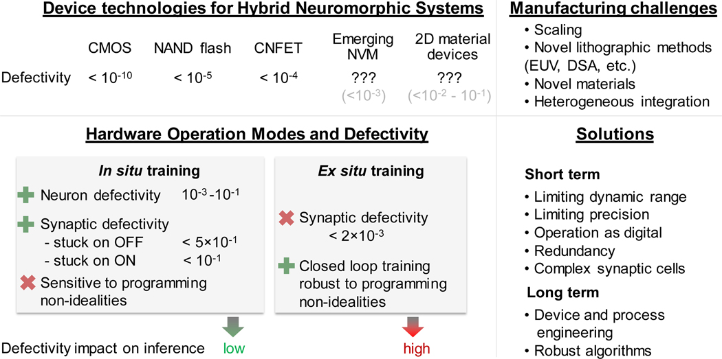
Figure 1.

Figure 1.

Defectivity ranges, tolerances, and mitigation actions for different operational modes. Defectivity ranges are approximate and sensitive to degree of redundancy, network design (for networks) and the precise technology and fabrication routes (for device technologies).

References:

  • 1.Big data needs a hardware revolution. Nature 554, 145–146 (2018). doi: 10.1038/d41586-018-01683-1 [DOI] [PubMed] [Google Scholar]
  • 2.Xia Q. and Yang JJ. Nature Materials 18, 309–323 (2019). doi: 10.1038/s41563-019-0291-x [DOI] [PubMed] [Google Scholar]
  • 3.Hu M. et al. Proceedings of the 53rd Annual Design Automation Conference. Art. No. 19. Austin, Texas. June 05-09, 2016. doi: 10.1145/2897937.2898010 [DOI] [Google Scholar]
Nanotechnology. 2021 Jan 1;32(1):012002.

Section 1 - Floating Gate Memory Based Hardware

Konstantin K Likharev 1, Dmitri B Strukov 2

Status

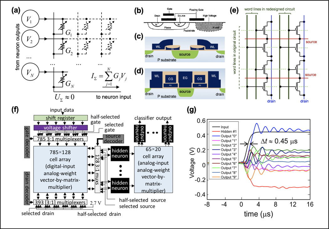
The present-day revolution in deep learning, triggered by the use of high-performance hardware, in turn has stimulated the development of even more powerful digital systems, specific for machine learning tasks. However, the use of digital operations for the implementation of neuromorphic networks, with their high redundancy and noise/variability tolerance, is inherently unnatural. Indeed, the performance of such networks may be dramatically improved using analog and mixed-signal integrated circuits. In this approach, the key operation - the vector-by-matrix multiplication (VMM) - is implemented on the physical level in a crossbar circuit, using the fundamental Ohm and Kirchhoff laws (Fig. 1a) [1].

Figure 1.

Figure 1.

(a) Generic scheme of analog vector-by-matrix multiplication in a crossbar circuit with adjustable crosspoint devices. For clarity, the output signal is shown for just one column of the array. (b-d) Schematic cross-sections of (b) synaptic transistor, and (c) ESF1 and (d) ESF3 supercells. ESF stands for Embedded SuperFlash NOR flash memory technology. Such technology is based on array of supercells, with each supercell hosting two split-gate floating-gate transistors. (e) 2×2 fragment of the ESF1 supercell array, highlighting the routing of word lines in the original NOR flash memory (dashed green lines) and in the array modified for analog applications (solid green lines). (f) Network for classification of MNIST benchmark images, with 105+ FG cells, implemented in 180-nm technology, and (g) the typical dynamics of the network’s input signal, the output of a sample hidden-layer neuron, and all network’s outputs, after an abrupt turn-on of the voltage shifter’s power supply [6].

The main difference between numerous recently demonstrated circuits of this type is the choice of crosspoint devices with adjustable conductance G - essentially analogue nonvolatile memory cells, storing the pre-recorded synaptic weights wG. Much recent effort is devoted to using, in this role, memristors and other novel two-terminal nanodevices, some of which may enable scaling beyond the 10-nm frontier [2]. However, the fabrication technology of such devices is still immature for their VLSI integration. It turned out that quite comparable results may be obtained using much more mature floating-gate (FG) memory cells.

Up until recently, such devices were implemented mostly as “synaptic transistors” (Fig. 1b) [1, 3], which may be fabricated using standard processes available from CMOS foundries. This approach has enabled the implementation of several sophisticated systems [35]. However, these devices have relatively large areas (> 1000F2, where F is the minimum feature size), leading to higher interconnect capacitances and hence larger energy losses and time delays. Recently, it was proved [2, 6] that much better results may be obtained re-designing, by simple re-wiring (Fig. 1e), the arrays of the ubiquitous flash memories with their highly optimized cells. The areas of the so-modified arrays of the ESF1 and ESF3 NOR flash memories (Fig. 1b, c), with the latter technology scalable to F = 28 nm, are close to 120F2 and may be further reduced to ~40F2. The synaptic weights of FG cells in the modified arrays may be individually fine-tuned with accuracy better than 1%.

This approach was successfully demonstrated on a medium-scale (28×28-binary-input, 10-output, 3-layer, 101,780-synapse) network for pattern classification (Fig. 1 f, g) [6]. Remarkably for such a first attempt, still using the older ESF1 180-nm technology, the experimentally measured time delay and energy dissipation (per one pattern classification) were below, respectively, 1 μs and 20 nJ, i.e. at least three orders of magnitude better than those obtained with the 28-nm digital TrueNorth chip used for the same task, with a similar fidelity. Preliminary experimental results for the chip-to-chip statistics, long-term drift, and temperature sensitivity of the network are also encouraging [6].

Current and Future Challenges

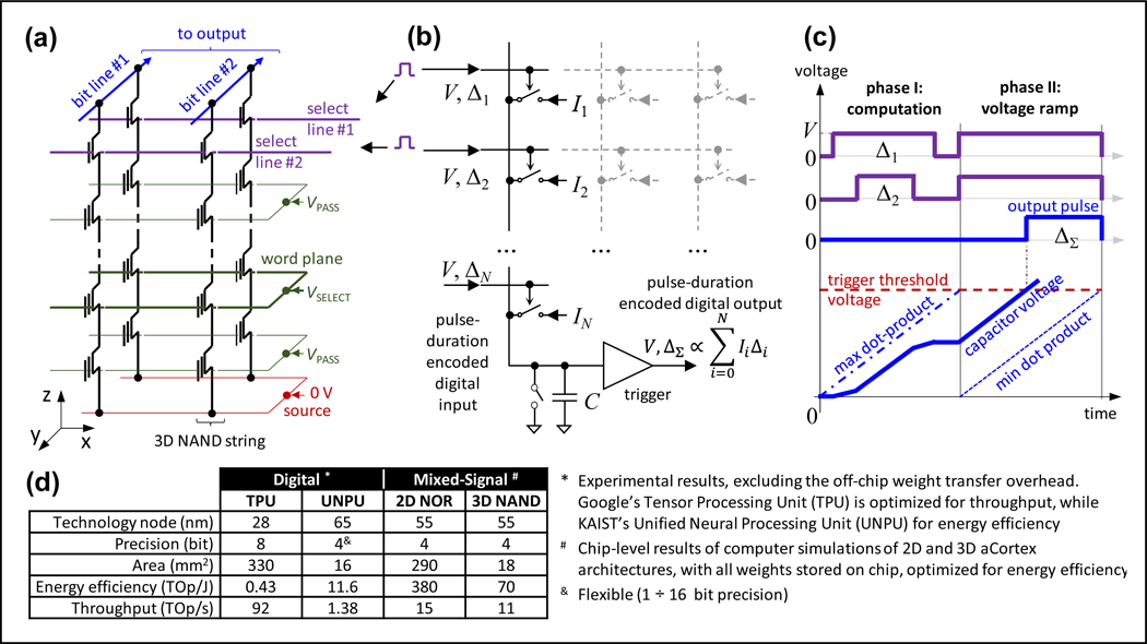
There are at least two major current challenges to this approach. First, it has to be employed to implement practically useful general-purpose, reconfigurable neuromorphic processors. The recent architectures addressing this challenge (e.g., the aCortex [2]) are typically based on rectangular arrays of analogue FG crossbars performing the VMM function, connected via digital interfaces to the main memory used for storing input, output, and intermediate data. Such architecture allows storing synaptic weights locally, thus avoiding performance-penalizing communications with the off-chip memory. Not surprisingly, already first simulations of the aCortex, based on experimental data from prototype VMM circuits, have shown significant advantages in energy efficiency over its digital counterparts (Fig. 2d), which would be even more dramatic with proper account of the off-chip data transfer overhead in digital systems. (Furthermore, simulations have shown that similarly superior energy efficiency may also be reached in mixed-signal neuromorphic circuits based on industrial-grade SONOS FG memories [8, 9].) We expect that the forthcoming re-optimization of the aCortex architecture for speed, using much larger parallelism, will yield a computational throughput much higher than that of state-of-the-art digital systems, including Google’s TPU (Fig. 2d).

Figure 2.

Figure 2.

(a) 3D NAND flash memory circuit consisting of vertical strings of NAND cells. Here, a time-domain VMM operation may be performed simultaneously with all cells of one x-y layer, selected by applying a smaller voltage to a specific word plane, while keeping all other word planes biased with larger “pass” voltage. (b) Time-domain vector-by-matrix multiplication scheme, and (c) its timing diagram. On panel (b), the adjustable current sources describe the FG cells of a particular layer, while the inputs are pulse-duration-encoded enable signals applied to the select transistors that connect each 3D NAND string to a bit line. (d) Comparison of general-purpose neuromorphic accelerators, evaluated on inference tasks of comparable complexity, at similar functional accuracy [10].

The second current challenge is the extension of the FG approach to larger deep networks. Perhaps the most exciting opportunity for such extension is presented by the modern 3D NAND circuits, already featuring up to 96 layers of FG cells, resulting in an unparalleled areal density. The current structure of such 3D circuits, with the shared word planes (Fig. 2a) does not allow one to address each FG cell individually using the generic VMM scheme shown in Fig. 1a. However, this problem may be resolved using the time-domain approach [7, 10] illustrated in Fig. 2b,c. Detailed simulations of a mixed-signal neuromorphic aCortex processor based on the time-domain VMM, with 64-layer gate-all-around macaroni-type 3D-NAND memory cells, have shown that due to higher parasitics, its energy efficiency is somewhat worse than that of the 2D aCortex (Fig. 2d). On the other hand, the 3D aCortex has a much (~100x) higher weight storage capacity per unit chip footprint area – the factor which may be crucial for larger neuromorphic models.

In the long term, the main challenge is to extend the FG approach to much larger neuromorphic systems performing cognitive tasks more complex than pattern classification, including flexible hardware tools for fast modelling of novel network architectures and brain function models.

Advances in Science and Technology to Meet Challenges

Meeting this long-term challenge would require a large-scale multi-disciplinary effort focused on synergistic development of algorithms, hardware circuits, and architectures, notably including the following aspects:

  • development of novel neural models and training algorithms that would ensure their efficient mapping onto the co-designed hardware architectures, with account of device and circuit imperfections;

  • re-engineering of 3D FG memory blocks, that would allow simultaneous addressing extended sub-sets of FG cells, possibly using area-distributed interfaces with external circuits; and

  • re-optimization of FG cells for their use in neuromorphic circuits, in particular to decrease variations of the subthreshold slope, and to reduce the drain-induced barrier lowering.

Another important task is the development of efficient testing concepts, algorithms, and circuits, which would allow fast and reliable detection of device and circuit defects and imperfections.

Concluding Remarks

First experimental results and detailed computer simulations using reliable device models have shown that mixed-signal implementations of deep neuromorphic networks, based on industrial-grade floating-gate memory cells, may be much faster and more energy-efficient than their digital counterparts. Moreover, such FG circuits may have areal density exceeding that of chips based on 1T1R memristive devices, at much more mature technology. We believe that further development of the FG approach may lead to neuromorphic VLSI circuits with unprecedented performance on real-world cognitive tasks.

Acknowledgements

Authors would like to thank M. Bavandpour, M.R. Mahmoodi, and S. Sahay for letting us to include unpublished results, and acknowledge funding from DARPA, Samsung, Google, and NSF.

References

  • [1].Hasler P, Diorio C, Minch BA and C. and Mead A 1994. Single transistor learning synapses Advances Neural Information Processing Systems 7 817–24 [Google Scholar]
  • [2].Bavandpour M, Mahmoodi MR, Nili H, Merrikh Bayat F, Prezioso M, Vincent A, Strukov D, and Likharev KK 2019. Mixed-signal neuromorphic inference accelerators: Recent results and future prospects IEEE Int. Electron Device Meeting (San Francisco, CA: ) pp. 20.4.1–4 [Google Scholar]
  • [3].Hasler J and Marr H 2013. Finding a roadmap to achieve large neuromorphic hardware systems Frontiers Neurosci. 7 118. [DOI] [PMC free article] [PubMed] [Google Scholar]
  • [4].Chakrabartty S and Cauwenberghs G 2007. Sub-microwatt analog VLSI trainable pattern classifier IEEE J. Solid-State Circuits 42 1169–1179 [Google Scholar]
  • [5].Lu J, Young S, Arel I, and Holleman J 2015. A 1 TOps/W analog deep machine-learning engine with floatinggate storage in 0.13 μm CMOS IEEE J. Solid-State Circuits 50 270–281 [Google Scholar]
  • [6].Guo X, Merrikh Bayat F, Bavandpour M, Klachko M, Mahmoodi MR, Prezioso M, Likharev KK and Strukov D 2017. Fast, energy-efficient, robust, and reproducible mixed-signal neuromorphic classifier based on embedded NOR flash memory technology IEEE Int. Electron Device Meeting (San Francisco, CA: ) pp. 6.5.1–4 [Google Scholar]
  • [7].Bavandpour M, Mahmoodi MR, and Strukov D 2019. Energy-efficient time-domain vector-by-matrix multiplier for neurocomputing and beyond IEEE Trans. Circuits System. II 22 1512–1516 [Google Scholar]
  • [8].Fick L, Blaauw D, Sylvester D, Skrzyniarz S, Parikh M, and Fick D 2017. Analog in-memory subthreshold deep neural network accelerator IEEE Custom Integrated Circuits Conf. (Austin TX: ) pp. 1–4 [Google Scholar]
  • [9].Agarwal S, Garland D, Niroula J, Jacobs-Gedrim RB, Hsia A, Van Heukelom M S, Fuller E, Draper B and Marinella M 2019. Using floating gate memory to train ideal accuracy neural networks IEEE J. Explor. Solid-State Computat. Devices Circuits 5 52–7 [Google Scholar]
  • [10].Bavandpour M, Sahay S, Mahmoodi MR and Strukov D 2019. 3D-aCortex: An ultra-compact energy-efficient neurocomputing platform based on commercial 3D-NAND flash memories ArXive (submitted) [Google Scholar]
Nanotechnology. 2021 Jan 1;32(1):012002.

Section 2 - Materials consideration for emerging devices

Hao Jiang 1, Thomas Mikolajick 2, Damien Querlioz 3, Martin Salinga 4

Status

History:

A decisive part of any machine learning system is the semiconductor memory. This needs to be brought as close as possible to the computing function to overcome the von-Neumann bottleneck. Traditionally, all semiconductor memories like SRAM, DRAM or EPROM or Flash memories were based on the principle of charge storage. However, since the late 1990s the efforts of using several different switching effects that utilize specific material properties have increased [1], putting material science at the heart of the research activity in non-volatile memories. Ferroelectric switching, magnetic switching, phase change and memristive switching based on ion movement have become the focus point for research and development in new non-volatile semiconductor memories (see fig. 1). The widely used materials for ferroelectric switching, phase change and ion movement based memristive switching are traditional perovskite-based (e.g. Pb(Zr,Ti)O3) and recently-discovered HfO2-based ferroelectrics, chalcogenide glass materials frequently involving Ge/Te/Sb, and transition metal oxides (e.g. HfO2 and TaOx), respectively. For magnetic switching devices, the magnetic layers are usually made with Fe and/or Co while MgO is typically used as the tunnelling barrier layer in between. Note that all of the mentioned physical mechanisms with the exception of ferroelectric switching use a resistance based readout [2]. While in ferroelectric tunnelling junctions, the material state can be read out by the resistance as well, the preferred readout of a ferroelectric is either by measuring the switched charge or by coupling the ferroelectric to a field effect transistor [3]. In the last years, it has been established that the same mechanisms might be very well suited to realize functions required for machine learning. However, while for a semiconductor memory an abrupt switching with a clearly defined threshold is most favourable, the optimum switching characteristics needed for machine learning systems are still an intense field of research, depending on the targeted application (inference or learning), and requiring a strong link across the hierarchy levels starting at the material level all the way up to the system level. For all mechanisms mentioned above, the research activities go back to the 1960s and first low or medium volume non-volatile memory products exist in the marketplace.

Figure 1.

Figure 1.

Variants of switching mechanisms used for emerging non-volatile memories. a) In ferroelectric switching the dipoles of a ferroelectric material are switched by an electrical field. b) In a magnetic tunnel junction the magnetization of a free layer is switched between the parallel and anti-parallel orientation towards a fixed reference layer. c) In phase change memories the phase of a chalcogenide is switched between amorphous and crystalline using joule heating and (d) in ion movement based memories a conductive filament made of metal atoms or oxygen vacancies is reversibly formed and ruptured.

What will be gained with further advances:

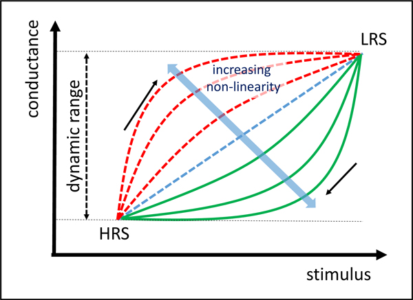
In a traditional computing system using the von-Neumann architecture, speed and energy efficiency is becoming limited by the transfer of data via the memory bus. Therefore, approaches moving the computation closer to the memory cell itself are highly desired. The first step can be considered as “logic-in-memory”. Here, the computation is done directly in the memory array by using the stored data as one input variable and using either a suitable circuit or a pulsing scheme to realize the logical function to have the result in the memory again. All resistive switching approaches are suitable here and also variants with ferroelectric switching have been shown. In the next step, the memory device can be used to simplify the calculation of weights in artificial neural networks (ANNs). Using Ohm’s and Kirchhoff’s law, analogue vector matrix multiplications can be achieved in resistive memory arrays and many lab demonstrations have already been made using approaches based on phase change and ionic movement [4,5,6]. Finally, spiking neural networks (SNNs) require both to mimic the function of a neuron and a synapse. Synapses have been achieved using all of the physical effects shown in Fig. 1. Neurons were realized based on ferroelectric switching, phase change and threshold-switching type memristive devices (e.g. based on NbOx) [2,7], and using the nonlinear dynamics of magnetization in magnetoresistive nanodevices [8,9]. Learning-capable hardware is the most demanding on the material side: intense research is still required, as for synapses an analogue and linear behaviour (see Fig. 2) is highly desirable [4]. Both analogue and accumulative switching were not in the focus of the traditional non-volatile memory device research and development.

Figure 2.

Figure 2.

SET (red curves) and RESET (green curves) of a switch for use in a synapse for SNN or a weight device for ANN. Ideal characteristics for the usage as weight is added in blue.

Status:

For a memory array utilizing one of these physical mechanisms, next to the memory cell, a selection device is needed to handle disturbances. The simplest version for the selector device is a MOS transistor, which is used in ferroelectric RAMs, in magnetoresistive RAMs as well as in the available products using ion-movement based switching. However, using a MOSFET selector the memory cell needs to be connected directly to the silicon. For gaining extremely high densities, three-dimensional architectures, where the cells are stacked on top of each other, have become very popular since the first introduction of 3D NAND Flash in 2013. Therefore, other selector devices have moved into the focus of research. Especially threshold switching devices are intensively researched and used in the second-generation phase change memory devices under the name of 3D cross point memory. Ovonic threshold switching based on chalcogenides, metal-insulator transition, and metal-ion/oxygen-vacancy movement based switching in combination with a thermal runaway effect as observed in NbOx are all explored in this context [2].

Current and Future Challenges

Looking forward, three important research challenges need to be solved from the material point of view: (I) tuning the switching and reading characteristics beyond pure memory, (II) scaling the device density and (III) stability and reliability. Here stability describes the consistent behaviour or reproducibility of the material stack after writing operation not considering the degradation that will happen during operation. Reliability, in contrast, describes the degradation of the cell states during storage (retention), repeated writing (endurance) or parasitic stimuli (disturbs) of the cell. Depending on the specific device type, different materials issues need to be solved. For example, for HfO2-based ferroelectric devices, the wake-up and imprint issues as well as the improvement of cycling endurance worth further studies; in phase-change-based devices, the material compositions are observed to fluctuate significantly due to the high temperatures and strong electric fields involved in the switching processes; for ion movement based memristive switching devices, there are concerns in the metal electrode stability and the trade-off between operation current and state retention; magnetic tunnel junctions are made with multi-layers of ultra-thin films, posing a serious challenge to the growth and etching processes.

With respect to the switching and reading characteristics a strong interaction of the material centric device research with the upper layer circuit and system design is required, as in a machine learning system, the most suitable device characteristics cannot be defined without looking at the system performance, and can depend tremendously on the targeted application. Fig. 2 summarizes one important aspect on the single device level that has been extensively studied in the last 3–4 years for developing learning-capable hardware neural networks and that illustrates that additional material optimization beyond the established memory function is required [4]. However, also the interaction between write and read, stability aspects as well as the ability to integrate the device into an array or distributed architecture play a crucial role here. Especially for inference tasks in ANNs it is important to note that highly parallelized operation is a must. Therefore, in contrast to traditional memory arrays, where a rather high read current is necessary to achieve a fast readout, a smaller read current is indeed desirable. This could be an opportunity for technologies like ferroelectric tunnel junctions that suffer from a limited read current when pure memory operation is the task.

Device scaling has shifted gears in the last years from purely increasing the device count by reducing the dimensions towards using the third dimension and more and more levels per cell. Recently in 3D NAND, 16-level devices (4 bits per cell) have entered mass production. These trends somewhat reduce the stringent requirements for device size reduction, but cannot make it obsolete, as the economics require achieving the highest possible functionality per real estate. Nevertheless, both aspects need to be considered. The device needs to show the desired behaviour at dimensions in the 10–20nm regime, which implies that the films need to be in the nm thickness range, and it must be possible to stack many layers on top of each other to achieve the necessary density for complex machine learning systems. The latter implies that a selector element not connected to the silicon bulk must be available and that suitable deposition techniques to realize high quality layers on materials used in standard CMOS processing are established.

Stability and reliability are traditionally the main challenges to bring a non-volatile memory into high volume production. Therefore, magnetic random-access memories, phase change memories and especially ion movement based memories have required about a decade of very intense development to come up with first niche products for the general market. However, with respect to machine learning applications we need to handle even more critical issues. If we want to tailor the current-voltage characteristics to make analogue computing functions possible, we need to guarantee the stability to a much higher degree compared to digital or even multi-level devices where we can rely on the high margin between different states.

Advances in Science and Technology to Meet Challenges

The development of semiconductor devices in general and memory devices in particular has come a long way to deliver devices with 10–20 nm feature sizes. In terms of film production, highly reproducible techniques like atomic layer deposition have enabled the progress in the last 1–2 decades and still have strong contributions to solve the challenges described above. Especially in scaled down devices we need to consider that local fluctuations of the composition may transfer to device variability. Therefore, reducing the number of components in the active switching layer is crucial. In ferroelectric memories, binary oxides based on HfO2 have become much more popular compared to the traditional perovskites [3] which have at least three, but more commonly, four components. In phase change devices, even monoatomic solutions are perused to reach the ultimate device [10]. Ultimately, we might need to introduce new physical mechanisms to master the challenges observed during the implementation. Magnetic random access memories can act as a role model here with the introduction of magnetic tunnel junctions, Spin-Torque transfer, perpendicular magnetization and in the future possibly spin orbit torque that were introduced in the last 25 years to finally be adapted by a significant number of semiconductor foundries.

Concluding Remarks

Machine learning makes non-volatile memory functions in electron devices even more important than they already are today. However, the specific requirements call for modified or even completely new solutions. At the end of an era of charge storage, finally the prime time for material related switching effects has come making material development even more critical than it has been for traditional electron devices in the past.

Acknowledgements

The research leading to this publication has received funding from the European Research Council (ERC) under the European Union’s Horizon 2020 research and innovation programme (grant agreement no 640003 and 715872).

References

  • [1].Mikolajick T. and Pinnow C-U, The Future of Nonvolatile Memories, Proc. Nonvolatile Mem. Technol. Symp. (JPL Publishing, Pasadena, CA: ), pp. 4–6 (2002). [Google Scholar]
  • [2].Slesazeck S. and Mikolajick T, Nanoscale resistive switching memory devices: a review, Nanotechnology, Volume 30, Number 35 (2019). [DOI] [PubMed] [Google Scholar]
  • [3].Mikolajick T, Slesazeck S, Park MH, and Schroeder U, Ferroelectric hafnium oxide for ferroelectric random-access memories and ferroelectric field-effect transistors. MRS Bulletin, 43(5), 340–346 (2018). [Google Scholar]
  • [4].Yu S, Neuro-inspired computing with emerging nonvolatile memorys, Proceedings of the IEEE, vol. 106, no. 2, pp. 260–285 (2018). [Google Scholar]
  • [5].Ambrogio S, Narayanan P, Tsai H, Shelby RM, Boybat I, di Nolfo C, Sidler S, Giordano M, Bodini M, Farinha NCP, Killeen B, Cheng C, Jaoudi Y, and Burr GW, Equivalent-accuracy accelerated neural-network training using analogue memory, Nature 558, 60–67 (2018). [DOI] [PubMed] [Google Scholar]
  • [6].Li C, Belkin D, Li Y, Yan P, Hu M, Ge N, Jiang H, Montgomery E, Lin P, Wang Z, Song W, Strachan JP, Barnell M, Wu Q, Williams RS, Yang JJ, and Xia Q, Efficient and self-adaptive in-situ learning in multilayer memristor neural networks, Nature Communications 9, 2385 (2018). [DOI] [PMC free article] [PubMed] [Google Scholar]
  • [7].Tuma T, Pantazi A, Le Gallo M, Sebastian A, Eleftheriou E, Stochastic phase-change neurons. Nature Nanotechnology 11, 1–8 (2016). [DOI] [PubMed] [Google Scholar]
  • [8].Romera M, Talatchian P, Tsunegi S, Abreu Araujo F, Cros V, Bortolotti P, Trastoy J, Yakushiji K, Fukushima A, Kubota H, Yuasa S, Ernoult M, Vodenicarevic D, Hirtzlin T, Locatelli N, Querlioz D, and Grollier J, Vowel recognition with four coupled spin-torque nano-oscillators, Nature, 563(7730), 230 (2018). [DOI] [PubMed] [Google Scholar]
  • [9].Mizrahi A, Hirtzlin T, Fukushima A, Kubota H, Yuasa S, Grollier J, and Querlioz D, Neural-like computing with populations of superparamagnetic basis functions. Nature communications, 9(1), 1533 (2018). [DOI] [PMC free article] [PubMed] [Google Scholar]
  • [10].Salinga M, Kersting B, Ronneberger I, Prasad Jonnalagadda V, Thang Vu X, Le Gallo M, Giannopoulos J, Cojocaru-Miredin O, Mazzarello R, Sebastian A, Monatomic phase change memory, Nature Materials 17, 681–685 (2018). [DOI] [PubMed] [Google Scholar]
Nanotechnology. 2021 Jan 1;32(1):012002.

Section 3 - Scaling of Emerging Hardware and Technology for Machine Learning

John R Erickson 1, Shuang Pi 2, Feng Xiong 3

Status

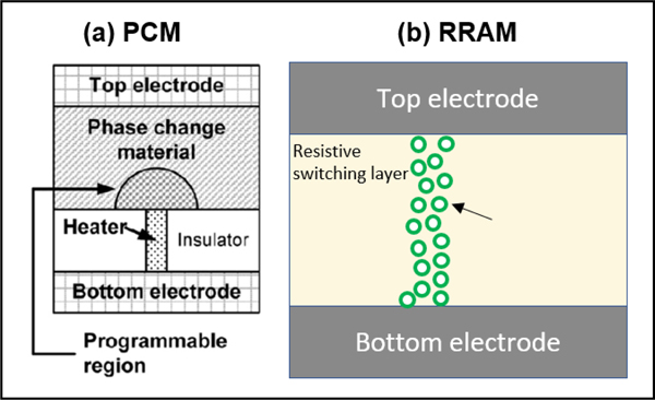
The human brain, which consumes only ~20 W of power and exceeds the petaflop mark, has been the inspiration for the next generation of computers [1]. As such, deep learning and artificial neural networks (ANNs) have been heavily investigated. However, the learning time and energy usage of these systems are orders of magnitude short of mimicking the brain. Part of the reason for this disparity in efficiency is the reliance on traditional CMOS circuitry elements for simulating neuronal actions, which requires bulky external memory components leading to a large device footprint and energy consumption. With this in mind, researchers are working towards building highly scalable hardware for ANNs that can replicate synaptic actions through encoding analog states in their programmable conductance levels [1]. An ideal synaptic device should offer low power, high precision, large dynamic range, fast speed, high scalability, non-volatile retention, good endurance, and low variations among many others [2]. Emerging memory devices such as phase change memory (PCM), resistive random-access memory (RRAM), conductive-bridging RAM (CBRAM), spin transfer torque RAM (STT-RAM), as well as electrochemical devices are all different classes of synaptic devices being investigated [1]. Limited in scope, this work will only focus on PCM and RRAM (Fig. 1), due to their relative closeness to large scale commercialization.

Figure 1.

Figure 1.

Working principles of phase change memory (PCM) and resistive RAM (RRAM) devices. Fig. 1a shows a cell, the active PCM area is in between a top and bottom electrode, including a heater to induce melt/quench cycles. As heat is applied the active channel will change its conductivity based on the phase of the channel. Reproduced with permission [4] Copyright 2010, IEEE. Fig. 1b shows a typical filamentary RRAM, as a writing current is applied to the cell, free ions move together to form a connection between the top and bottom electrodes. Reproduced with permission [1] Copyright 2019, John Wiley and Sons.

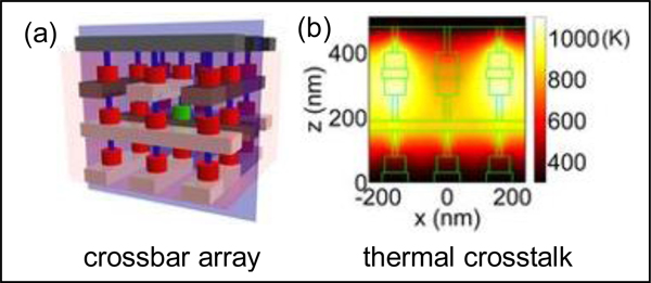
For ANN applications, the demanding function of vector-matrix multiplication can be efficiently implemented in a cross-point network [3] (Fig. 2a). The scale of the network, defined by the number of inputs multiplied by the number of outputs, determines its computing power. Both PCMs and RRAMs offer high device density, due to the inherently small footprint of cross-point cells. By further scaling these individual devices in sizes, massive increases in energy efficiency, speed, and network density can be expected. With these improvements, large scale integration of ANNs into common technologies can be achieved, leading to transformative advancements in machine learning, artificial intelligence, data analytics, internet of things (IoTs), and even flexible/wearable smart devices, radically changing the role that technology plays in everyday life.

Figure 2.

Figure 2.

(a) Schematics of a crossbar array. (b) Thermal crosstalk due to Joule heating in adjacent cells. Adapted with permission [3], Copyright 2015 Nature Publishing Group.

Current and Future Challenges

One formidable problem encountered in device scaling is thermal crosstalk, as illustrated in Fig. 2b [3]. PCM devices need to be elevated to a much higher temperature for melt/quench cycles [4], requiring a large amount of energy (10–100 pJ) for switching events. This heating process can unintentionally perturb the states of adjacent cells through thermal crosstalk, which will only become more extensive as energy densities as well as device densities get larger. Similarly, Joule heating is believed to be necessary for facilitating ion generation and mobility enhancement to form conduction channels and/or modulate conductive junctions in RRAMs. With operation of high-density RRAM arrays generating intensive local heating, thermal crosstalk limits the scaling potential of RRAM and needs to be addressed through both material engineering and overall system design to achieve better thermal stability.

Another challenge that is likely to be exacerbated with scaling is device reliability such as endurance, variation, and stability. Although individual PCM devices exhibit good endurances, the stochastic nature of the melt/quench cycle can lead to reduced device lifetimes, not only because of large variation in individual device performances, but also due to individual device degradations like resistance drift [5]. In addition, phase separation in the material can cause devices to stick in either SET or RESET, limiting endurance [5]. Aggressive scaling of PCM devices only serves to aggravate these issues, as the consistency of individual device compositions becomes increasingly difficult to achieve while keeping commercially plausible deposition rates [4]. Manufacturing high density RRAM device arrays with sufficient yield also becomes difficult. RRAM fabrication usually needs an etching metal layer together with multiple functional thin films. These can generate non-volatile by-products, contaminating the critical interface and introducing numerous variabilities, especially in smaller devices. In addition, as most RRAM materials require an electrical forming step to initialize conductance switching, controlling and eliminating such high stress processes will be critical for improving process yield.

Finally, higher interconnection resistances from smaller electrode linewidths reduce the readability of the conductance change in a multi-level PCM and RRAM devices. Small changes in the read current between these closely spaced conductance levels can easily be shadowed by noise [6]. In this case, additional compensation would be required to differentiate these subtle differences, which will reduce either precision or speed, limiting the accuracy and efficiency of a machine learning hardware based on such emerging devices.

Advances in Science and Technology to Meet Challenges

Optimizing the thermal efficiency of cells is the first step towards improving the energy efficiency of PCM devices and minimizing thermal crosstalk. Crosstalk typically occurs during the amorphization process, with the high heat required for melting accidentally crystallizing neighbouring amorphous cells. To minimize this risk as device densities increase, a material with low melting temperature and thermal conductivity can reduce the amount of heat spreading during the amorphization step; whereas a high crystallization temperature will increase the thermal stability of the device in the amorphous phase. Most efforts to increase the endurance of devices are focused on atomic-level engineering of these materials through the inclusion of dopants, though its viability in the nanoscale limit is still indeterminate [7]. To then further improve the endurance of PCM devices, materials with low volume changes during melt/quench cycles, as well as implementation of in-situ self-anneal heating during operations should be investigated [8].

To combat thermal crosstalk in RRAM systems, small operational currents has been demonstrated in several sub-10 nm material systems such as TiOx, TiOx/AlOx, HfO2, and WOx [6]. Filamentary RRAM devices typically demonstrate a constant thermal heating with device scaling because the size of the filamentary channel remains the same with reduction in device dimension. However, once the device footprint is scaled to be smaller than a typical filamentary channel (~10 nm), we expect to observe a limited channel growth and hence a reduction in programming current and Joule heating. While these observations imply a path to begin to address thermal crosstalk, building reliable device functionality is still challenging with higher device variability potentially associated with device and current scaling implied in pioneer works [9, 11].Electrical forming steps can also be eliminated with metal particle doping and other material engineering techniques. These could be further facilitated with atomic layer deposition to precisely control thin film composition and membrane quality [6].

For reducing wire resistance due to narrow interconnections, low dimensional conductive materials such as carbon nanotubes are showing progress. However, fabrication of high-density arrays remains challenging. Another solution is through building high aspect ratio metal electrodes with multilayer depositions, although the process is not currently commercially viable [9]. Beyond these, a 3D architecture to was demonstrated by splitting a network into vertically stacked multi-layer arrays. This configuration tremendously reduces the wire resistance, as well as its footprint, but raises integration questions [10]. Finally, alternative fabrication paths, including bottom up approaches as well as wafer bonding methods, have been investigated and should to be continued [9].

Concluding Remarks

Hardware implementation of ANNs is necessary to continue improving their performances. In this vein, several synaptic devices have been investigated, all with the potential for easy integration and size scaling. PCM and RRAM devices are discussed in this work because of their small footprint, analog conductive states, and relative technological maturity. Though both of these classes of devices have been heavily investigated, properly managing the energy usage, thermal crosstalk, reliability, and endurance of these devices remain as challenges, especially as these devices attempt to be reduced to the nanoscale dimensions. To this end, materials engineering, proper thermal management, and new device architectures are potential solutions towards these issues.

Acknowledgements

J.R.E. and F.X. acknowledge support through NSF Award ECCS-1901864 and CCF-1909797.

References

  • [1].Wan Q, Sharbati MT, Erickson JR, Du Y, and Xiong F, “Emerging Artificial Synaptic Devices for Neuromorphic Computing,” Adv. Mater. Technol, vol. 1900037, no. 4, pp. 1–34, 2019. [Google Scholar]
  • [2].Jeong H. and Shi L, “Memristor devices for neural networks,” J. Appl. Phys. D Appl. Phys., 2019. [Google Scholar]
  • [3].Sun P, et al. , “Thermal crosstalk in 3-dimensional RRAM crossbar array”, Sci. Rep. 5, 13504, 2015. [DOI] [PMC free article] [PubMed] [Google Scholar]
  • [4].Wong H-SP, Raoux S, Kim S, Liang J, Reifenberg JP, Rajendran B, Asheghi M, Goodson KE, Proc. IEEE 98, 2201, 2010 [Google Scholar]
  • [5].Burr GW et al. , “Recent Progress in Phase-Change Memory Technology,” IEEE J. Emerg. Sel. Top. Circuits Syst, vol. 6, no. 2, pp. 146–162, 2016. [Google Scholar]
  • [6].Xia Q. and Yang JJ, “Memristive crossbar arrays for brain-inspired computing”, Nat. Mater. 18, 309–323, 2019 [DOI] [PubMed] [Google Scholar]
  • [7].Phys A. et al. , “Improving the performance of Ge2Sb2Te5 materials via nickel doping : Towards RF- compatible phase-change devices,” Appl. Phys. Lett, vol. 171903, no. October, pp. 4–9, 2018. [Google Scholar]
  • [8].Khwa WS et al. , “A Novel Inspection and Annealing Procedure to Rejuvenate Phase Change Memory from Cycling-Induced Degradations for Storage Class Memory Applications,” in 2014 IEEE International Electron Devices Meeting, 2014, pp. 709–712. [Google Scholar]
  • [9].Pi S, et al. , “Memristor crossbar arrays with 6-nm half-pitch and 2-nm critical dimension”, Nat. Nanotechnol. 14, 35–39, 2019 [DOI] [PubMed] [Google Scholar]
  • [10].Strukov DB and Likharev KK, “CMOL FPGA: A reconfigurable architecture for hybrid digital circuits with two-terminal nanodevices”, Nanotechnology 16, 888–900, 2005 [Google Scholar]
  • [11].Hou Y, et al. “Sub-10 nm low current resistive switching behavior in hafnium oxide stack”, Appl. Phys. Lett. 108, 123106 (2016) [Google Scholar]
Nanotechnology. 2021 Jan 1;32(1):012002.

Section 4 - Heterogeneous integration of emerging device arrays

Peng Lin 1, Can Li 2

Status

Neuromorphic systems based on emerging device arrays perform matrix multiplications following physical laws with high parallelism [1]. However, it is suggested that these arrays themselves, which implement the synaptic connections in neural networks, may not for suffice the requirement of an entire hardware computing system, whereas other circuit components, either implemented by conventional silicon devices or other emerging devices, need to be heterogeneously integrated to fulfil the rest of functions. Building a complete heterogenous system raises some new design and manufacturing challenges but would be a necessary step to achieve large capacity, small latencies and high energy efficiency.

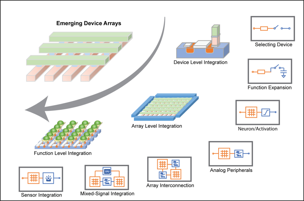
An overview of the integration roadmap is shown in Fig. 1, where different technologies can be heterogeneously integrated at the device level, the array level or the function level. First, the integration of other types of devices can directly enhance the electric performance of these emerging devices in large-scale operations and applications. For example, the integration of selectors (such as a transistor) promotes the reliability and the programmability of these synaptic devices [2][3], while a heterogeneous design of synaptic cells could facilitate high precision computing by minimizing the intrinsic variation effects in devices [4]. Meanwhile, active analog circuit components can be integrated at the array level to program (“update”) the synaptic weights stored in the emerging devices (as analog conductances or capacitances), and/or sense (“inference”) the output. Recently, demonstrations with integrated on-chip programming/sensing peripherals have shown encouraging results [5][6]. Moreover, the peripherals functions are not limited to accessing individual devices in an array. Neural network functions such as nonlinear activations and pooling can also be physically integrated at the array output and keep data movement locally. A promising approach would be harvesting the rich physical properties in emerging devices, which can potentially offer much improved speed and power efficiency as compared with the mature silicon technology [7]. Finally, in favor of emerging edge computing applications, the computing device arrays can be directly integrated with sensors, actuators, photonics, RF and control logics circuits with minimum communication and control overheads thus promise the real-time and low power edge processing [8].

Figure 1.

Figure 1.

Roadmap of heterogenous integration of emerging device arrays

Current and Future Challenges

One challenge for heterogeneous integration is the process compatibility. Many emerging devices involve an exotic material stack and/or a special fabrication process that require a high temperature. Therefore, they are sometimes difficult to be directly integrated with the mature silicon technology in the back-end processes. A compatible monolithic integration process generally calls for back-end-of-line compatibility which includes strict requirements on process temperatures and selection of materials. While GeSbTe based phase change materials and HfOx, TaOx based resistive switching materials have a better back-end process compatibility, others are not. For example spin-transfer torque magnetic memory cells use more than ten layers crystalline ferromagnetic materials[8][9], and fabricating lithium-based electrochemical devices require special encapsulation as lithium is highly reactive with silicon, therefore they are relatively challenging to be compatible with existing CMOS process. Alternative to specifically engineered monolithic integration process, circuit components could also be fabricated with different substrates through technologies such as low-temperature bonding, through-silicon via (TSV) interconnect, flip-chips, etc. For example, an image sensor array based on “III-V” compounds such as InGaAs cannot be directly grow on CMOS substrate due to high process temperature but can be assembled at packaging level through low-temperature bonding [11]. However, these assemble methods still require delicate designs and sometimes lead to limited inter-module bandwidth caused by larger parasitic. Lastly, the compatibility of the electrical properties between different integrated devices is equally important, which requires a systematic assessment of the requirements and the design capacity of each device or circuit component. For example, some emerging devices require high operating voltage and current and thus special design considerations are needed in designing the driving circuits especially with advanced silicon technology nodes.

Meanwhile, although the new computing paradigm has already eliminated the movement of weight matrices within the array, efficient data movement between arrays is still highly desired for large neural network applications. The efforts could involve optimized architecture designs such as local cache or global memory for storing temporal data, shared data bus or dedicated one-by-one connections between arrays and tiled arrays for different network topologies [12]. Meanwhile, developing efficient analog circuits for hardware functions, such as nonlinear activations and pooling functions, while keeping all the signals in the analog domain locally for inter-array communication, could significantly boost the efficiency to the next level if successful.

Advances in Science and Technology to Meet Challenges

First, the performance of the emerging system can still be largely affected by the device performance. Improvement of device performance (with compatible fabrication conditions) can significantly enhance the computing capability of these systems, and the figures of merits include the device uniformity, the analog conductance tuning linearity, the data retention, and the reprogramming endurance. Some effective solutions include advances in material engineering [13] or new cell designs with the integration of mature technologies [4].

Second, there is plenty of room to optimize the peripherals circuitry for higher energy efficiency and smaller footprint targeting a specific scenario. The different requirements of a neuromorphic system such as low precision and a specific voltage and current level may call for entirely different designs. Meanwhile, different array operating methods could be carefully compared and chosen, such as using pulse width or pulse amplitude for analog signal representation. In addition, emerging devices with various nonlinear behaviors may promise completely new designs and novel functions to be heterogeneously integrated and replace the conventional silicon devices and circuits entirely, with each device serving a unique functionality.

Finally, more efficient data communications can be implemented by new fabrication processes, new architectures, new array designs and more. For example, fabrication methods and array designs that reduce the wire resistances of the array can greatly promote the programming and inference precisions and mitigate the sneak path issues in passive (transistorless) arrays. 3D integration [14] of a heterogenous system is a favorable option as a lot of emerging devices can be compatibly stacked up (such as oxide-based memristors). The immediate benefit of a 3D system is shorter connection length and higher density. Different technologies can also be stacked on top of each other, promising significantly reduced system footprint, improved communication bandwidth (2D area interface as opposed to the 1D edge interface in 2D systems) and extended functionalities.

Concluding Remarks

The heterogenous integration of different emerging technologies is a key step towards the large-scale system integration and applications. The performance and efficiency of the system with all parts combined requires careful designs and optimizations. While promising proof-of-concept demonstrations were reported, challenges still exist in the integration process development, electrical compatibilities optimization and architectural designs for minimized data movement/conversion in modern neural networks. Extensive research efforts are underway to develop new emerging device types with unique functionalities, and smart circuit and array design with 3D integration are being investigated to make the system more efficient. The heterogenous integration of a wide spectrum of emerging devices, with new array and architecture designs promises the disruptive computing power for future machine learning and artificial intelligence systems.

References

  • 1.Xia Q. and Yang J, “Memristive crossbar arrays for brain-inspired computing”, Nature Materials 18, 309–323, 2019 [DOI] [PubMed] [Google Scholar]
  • 2.Li C, et al. “Analogue signal and image processing with large memristor crossbars”, Nature Electronics 1 (1), 52–59, 2019 [Google Scholar]
  • 3.Yao P, et al. “Face classification using electronic synapses”, Nature Communications 8, 15199, 2017 [DOI] [PMC free article] [PubMed] [Google Scholar]
  • 4.Ambrogio S, et al. , “Equivalent-accuracy accelerated neural network training using analogue memory”, Nature 558 (7708), 60–67, 2018 [DOI] [PubMed] [Google Scholar]
  • 5.Xue C, et al. “A 1Mb Multibit ReRAM Computing-In-Memory Macro with 14.6ns Parallel MAC Computing Time for CNN-Based AI Edge Processors”, Digest of Technical Papers – IEEE International Solid-State Circuits Conference, 388–390, 2019 [Google Scholar]
  • 6.Cai F, et al. “A fully integrated reprogrammable memristor-CMOS system for efficient multiply-accumulate operations”, Nature Electronics 2, 290–299, 2019 [Google Scholar]
  • 7.Wang Z, et al. “Fully memristive neural networks for pattern classification with unsupervised learning”, Nature Electronics 1 (2), 137–145, 2018 [Google Scholar]
  • 8.Makarov A, et al. “CMOS-compatible spintronic devices: a review.”, Semiconductor Science and Technology 31(11), 1–25, 2016 [Google Scholar]
  • 9.Sverdlov V, et al. “CMOS technology compatible magnetic memories.”, ISNE 2019, 1–2, 2019. [Google Scholar]
  • 10.Fuller E. et al. “Li-ion synaptic transistor for low power analog computing” Advanced Materials 29(4), 1604310, 2017. [DOI] [PubMed] [Google Scholar]
  • 11.Chen C. et al. “Wafer-scale 3D integration of InGaAs image sensors with Si readout circuits”, 2009 IEEE International Conference on 3D System Integration, 1–4, 2009. [Google Scholar]
  • 12.Ankit A, et al. “PUMA: A Programmable Ultra-efficient Memristor-based Accelerator for Machine Learning Inference”, Proceedings of the Twenty-Fourth International Conference on Architectural Support for Programming Languages and Operating Systems, 715–731, 2019 [Google Scholar]
  • 13.Choi S, et al. “SiGe epitaxial memory for neuromorphic computing with reproducible high performance based on engineered dislocations” Nature Materials 17, 335–340, 2018 [DOI] [PubMed] [Google Scholar]
  • 14.Shulaker M, et al. “Three-dimensional integration of nanotechnologies for computing and data storage on a single chip” Nature 547, 74–78, 2017 [DOI] [PubMed] [Google Scholar]
Nanotechnology. 2021 Jan 1;32(1):012002.

Section 5 - The processing strategies for memristor crossbar fabrication

Yu Chen 1, Shisheng Xiong 1

Status

While the need for mobile and fast computing in a smart society is ever growing, the semiconductor industry has been failing to exploit the power and efficiency provided by device scaling. Currently, we are witnessing a divergence of paths for future computing, with non-von Neumann architectures that are anticipated to significantly disrupt traditional CMOS technology. For example, commercial digital AI chips (TrueNorth and Loihi) developed by IBM and Intel, respectively, collocated the memory and processing units for a reconfigurable design. Recently, memristor-based analogue computing has been the focus of intensive research. Memristors arranged in a crossbar array provide a two-dimensional representation of a neural network, and have the advantages of greatly maximizing the device area density (2N lines and N2 devices) and unifying logic and memory for in-memory computing. Analogue or hybrid chips based on this network have proven to be extremely efficient (computing power efficiency up to over 10TOPS per watt) for pattern classification or online training of neural network algorithms [1]. At a fundamental level, this novel hardware can act as a dot-product engine for running vector-matrix multiplication (VMM) operations, which are very frequently used in deep learning algorithms [2].

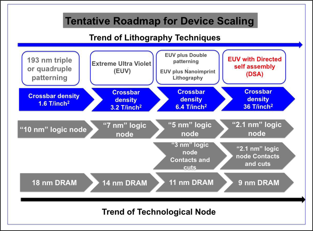
Since the first memristor device was made in HP Labs in 2008, different patterning techniques have been employed for memristor crossbar fabrication. Electron beam lithography (EBL) is more frequently used for patterning crossbar arrays at high resolution, but over a relatively small area [3]. Newly emerging techniques, including extreme ultraviolet (EUV) lithography, nanoimprint lithography (NIL) and directed self-assembly (DSA), have been listed in the International Roadmap for Devices and Systems (IRDS) as advanced lithography techniques for device fabrication at the 3–5 nm technology node (Figure 1) [4]. So far, direct templating with DSA (coupled with NIL) for the fabrication of bit patterned media with a crossbar structure has achieved a device density greater than 1T/inch2 [5]. The high-throughput advanced lithography techniques (e.g. EUV) will penetrate into the manufacturing once the market size and the fabrication cost are leveraged. For reference, in Figure 1 we have listed the estimated device density of passive crossbar arrays fabricated with the corresponding processing strategies. Considering the footprint of accessing devices, the cell area with respect to different architectures would be 8- or 4- fold larger: ~8F2 for one-transistor, one-resistor architecture (1T1R), 4F2 for one-selector, one-resistor architecture (1S1R), where F is the half pitch.

Figure 1.

Figure 1.

Tentative roadmap for crossbar density, along with logic and memory device scaling, according to the International Roadmap for Devices and Systems.

Current and Future Challenges

The continued downscaling of nanoelectronic devices imposes ever-more stringent requirements on the strategy used to achieve ultra-small feature size while maintaining low defectivity. Along with the previous success of memristor-based AI chips, it is becoming imperative to continue to increase the crossbar density for better network performance. The main challenges experienced in the scaling process of crossbar fabrication include the selection of proper processing strategies for sub-10 nm patterning, the increase in integration difficulty, and the potential for performance degradation of the miniaturized devices.

Current chip-level crossbar arrays are made at the μm level with conventional photolithography. Direct writing tools, such as EBL, are able to deliver high-resolution patterning, but are not ideal for mega-scale crossbar fabrication due to their extremely time-consuming writing procedure [6]. Furthermore, the small critical dimension of a crossbar causes the performance of the final device to be vulnerable to process variation. Therefore, it is critical to simultaneously optimize all the processing steps to reduce the defectivity and to enhance the pattern transfer uniformity. In addition, system-level integration requires reliable 3D integration of crossbar arrays with underlying CMOS circuits. Direct fabrication of crossbar arrays on a foundry-developed CMOS chip should guarantee precise alignment and a low thermal budget [7].

Another big challenge associated with crossbar scaling is the increasing density of local interconnects. The resistance of these non-ideal interconnects increases as the size shrinks, causing a significant voltage drop across the array. This phenomenon will severely disturb the functionality of memristor crossbar arrays, resulting in insufficient power supply on individual devices and a large error rate during write/read operations [8]. Other problems include more device-to-device variation and current interference between more densely packed neighboring cells, known as the sneak path current problem [9]. Although there is no description of the benchmark for defect density in the literature, the essence of neural network indicates that the defectivity level of a crossbar array can be higher than it can be for the logic chips, which are permitted less than 100 defects per cm2 [1]. The strategies to realize high-throughput manufacturing of large-scale, high-density crossbar arrays and integrated systems rely on the continued efforts to explore new patterning methodologies, as well as a collaborative effort between academia and industry.

Advances in Science and Technology to Meet Challenges

Both academia and industry are making long-term endeavors to realize the fabrication of large-scale, high-density crossbar arrays for production. EUV is a commercialized, high-resolution lithography technique for high-volume manufacturing in the semiconductor industry, which greatly simplifies the patterning process compared to 193i lithography using multiple patterning steps, but the cost of EUV remains high up to now [4]. For research, low-cost lithography techniques, such as NIL and DSA, can also enable high-resolution patterning. As a direct contact lithographic method, NIL has easily overcome the optical limits of conventional photolithography and the proximity effects observed in EBL. The NIL molds can be used repeatedly, allowing mass production of a crossbar structure in a highly cost-effective way. To date, NIL has been successfully applied in the direct fabrication of memristor crossbar arrays on top of a foundry-made CMOS chip with optimized planarization techniques [7].

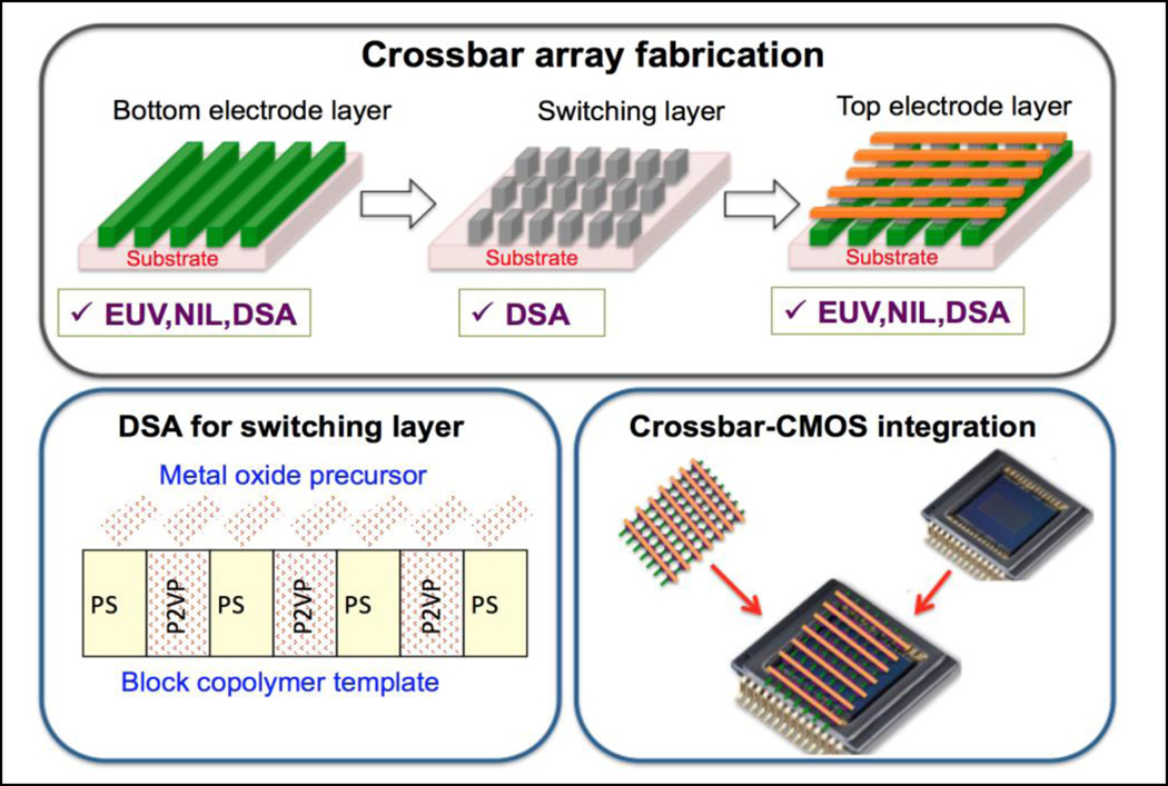
The recent advances in DSA of a block copolymer and subsequent pattern transfer are readying this technique for the fabrication of memristive devices. The assembled block copolymer thin film can function as an etching mask to transfer the pattern to the underlying layers. DSA is suitable for making either the electrodes or switching layers for crossbar memristive device arrays. Electrode fabrication can be realized in a metal lift-off process or a liquid-immersion metallization process. The metal elements can vary from Pt to Cu, Co, Ni, or others. DSA of cylinder-forming block copolymers (e.g. PS-b-PMMA or PS-b-P2VP), combined with sequential infiltration synthesis (SIS) offers an efficient way of patterning the switching layer for crossbar arrays. In SIS, a metal oxide precursor diffuses and selectively binds to reactive sites in the microdomain of the polar block [10]. SIS in combination with DSA, has been used to convert assembled block copolymer domains into oxides such as TiO2, Al2O3, ZnO, ZrO, HfO2, and WO2. With accurate control of both composition and uniformity, this combined process helps to address the leakage current issue by confining the conductive filament in nanometer-sized channels. By exploring various processing strategies as shown in Figure 2, it is expected that the key obstacles of device downscaling and system integration can be overcome, which paves the way for industrialization of crossbar fabrication in the near future[8].

Figure 2.

Figure 2.

Strategies for memristor crossbar arrays fabrication and integration with underlying CMOS devices.

Concluding Remarks

Memristive crossbar array devices will undergo a miniaturization process similar to that of the transistor as they are developed, so to implement the neuromorphic computing or memory, and they will simultaneously experience a reduction in power consumption and cost. Alternative lithographic techniques such as NIL and DSA fit in perfectly with the fabrication of high-density, periodic, and defect-tolerant crossbar arrays. These low-cost manufacturing methods are fully compatible with current semiconductor manufacturing processes, such that they are suitable for a back-end-of-line (BEOL) process in the integration of CMOS and crossbar arrays. In the future, 193i, or even EUV, may be used for high-throughput manufacturing of memristor-based AI chips. Combining lithography with stamp transfer or inkjet printing, we are able to create a crossbar structure on flexible substrates. The adoption of large-scale memristor arrays in the next generation of computing in the Artificial intelligence of Things (AIOT) era should provide exceptional performance.

Acknowledgements

Shisheng Xiong acknowledges the support by National Natural Science Foundation of China via Award No. 62974030. We acknowledge the Shanghai Municipal Science and Technology Commission for the one-belt one-road international cooperation grant and Fudan University for the seeding grant.

References

  • [1].Xia Q. and Yang JJ, “Memristive crossbar arrays for brain-inspired computing,” Nat. Mater, vol. 18, no. 4, pp. 309–323, Apr. 2019. [DOI] [PubMed] [Google Scholar]
  • [2].Li C. et al. , “Analogue signal and image processing with large memristor crossbars,” Nature Electronics, vol. 1, no. 1, p. 52, Jan. 2018. [Google Scholar]
  • [3].Khiat A, Ayliffe P, and Prodromakis T, “High Density Crossbar Arrays with Sub- 15 nm Single Cells via Liftoff Process Only,” Scientific Reports, vol. 6, p. 32614, Sep. 2016. [DOI] [PMC free article] [PubMed] [Google Scholar]
  • [4].Liu C-C et al. , “Directed self-assembly of block copolymers for 7 nanometre FinFET technology and beyond,” Nature Electronics, vol. 1, no. 10, p. 562, Oct. 2018. [Google Scholar]
  • [5].Xiong S. et al. , “Directed self-assembly of high-chi block copolymer for nano fabrication of bit patterned media via solvent annealing,” Nanotechnology, vol. 27, p. 415601, Oct. 2016. [DOI] [PubMed] [Google Scholar]
  • [6].Kirtaev R, Matveyev Yu., Fetisova A, Negrov D, and Zenkevich A, “Combined optical/e-beam lithography approach for the development of HfO2-based memristors in crossbars,” in 2015 International Conference on Memristive Systems (MEMRISYS), 2015, pp. 1–2. [Google Scholar]
  • [7].Xia Q. et al. , “Nanoimprint lithography enables memristor crossbars and hybrid circuits,” Appl. Phys. A, vol. 121, no. 2, pp. 467–479, Nov. 2015. [Google Scholar]
  • [8].Rofeh J. et al. , “Vertical integration of memristors onto foundry CMOS dies using wafer-scale integration,” in 2015 IEEE 65th Electronic Components and Technology Conference (ECTC), 2015, pp. 957–962. [Google Scholar]
  • [9].Li C. et al. , “Three-dimensional crossbar arrays of self-rectifying Si/SiO2/Si memristors,” Nature Communications, vol. 8, p. 15666, Jun. 2017. [DOI] [PMC free article] [PubMed] [Google Scholar]
  • [10].Waldman R, Mandia D, Yanguas-Gil A, Martinson A, Elam J, and Darling S, “The chemical physics of sequential infiltration synthesis—A thermodynamic and kinetic perspective,” The Journal of Chemical Physics, vol. 151, p. 190901, Nov. 2019. [DOI] [PubMed] [Google Scholar]
Nanotechnology. 2021 Jan 1;32(1):012002.

Section 6 - Defectivity and its impact on hardware neural networks

BD Hoskins 1, MW Daniels 1, A Madhavan 1,2, JA Liddle 1, JJ McClelland 1

Status

The current state of the art in electronics manufacturing is driven by achieving low defect rates, high levels of device-to-device uniformity, and binning integrated circuits by quality. As the industry pushes digital logic to below 5 nm in transistor channel length, new lithographic methods are needed to facilitate that scaling. Extreme ultra-violet (EUV) Lithography and directed self-assembly (DSA) are among such methods, but suffer from intrinsic limitations, such as stochastic photon illumination or assembly defects, respectively. These push the defect rates (of open connections, shorts, and other circuit-killing defects) to above the 0.01 cm−2 densities required for economical semiconductor manufacturing. Enabling logic to follow memory into the backend-of-line can relax feature-size-induced manufacturing problems. At the same time, this introduces new challenges in the 3D integration, particularly if similar areal densities are required. This is especially true in systems requiring new, CMOS compatible materials which suffer from defects absent in single crystal silicon.

Recent advances in neuromorphic computing, meanwhile, offer a bridge to a new era of ultra-dense, 3D-integrated computing architectures. These are largely based on a new suite of materials and manufacturing methods long thought to be unacceptable for digital manufacturing. Neuromorphic architectures, especially those based on nanodevice memories, have the benefit of massive redundancy in the number of possible solutions to a problem. This makes it possible to find solutions which either disregard or actively compensate for underlying hardware issues. The opportunities afforded by the low-precision, defect tolerant nature of neuromorphic computing, still an active topic of study at the algorithmic level, are beginning to manifest on the hardware and manufacturing stages as well.

Neuromorphic computing, therefore, offers a set of design freedoms that enable a radical departure from the typical manufacturing constraints of the past. While the error rates for conventional digital logic in CMOS are astronomically small, less than <10−10 based on the requirement that billions of transistors function on a single integrated circuit, the yields of even currently existing technologies, such as 3D-NAND, which often ship with a small percentage of defect memory blocks, suggests defectivities orders of magnitude higher near 10−5. Emerging technologies like carbon nanotube field effect transistors and resistive switches have been implemented in working demonstrations suggesting defectivities less than 10−4, but nevertheless may not achieve significantly higher levels of perfection[1], [2]. These emerging technologies may be able to find profitable new avenues for growth in emerging neuromorphic architectures as memory and logic merge.

Current and Future Challenges

Analog deep neural networks are based on dense nanodevice memories, but these systems are prone to defects both from the nanodevices as well as from variations in the underlying CMOS. In the long term, in situ training — training the network on the hardware in which it’s deployed—will yield systems resilient to these issues. In in situ training, defects that would nominally affect inference—that is, the classification action taken by the hardware — will be actively compensated for by the training routine. Several studies suggest that systems trained in situ can tolerate defectivity rates as high as 50% in missing synapses (significantly less tolerance for stuck-on devices, closer to 10%) and 0.1% to 10% in problematic neurons depending on the degree of redundancy, with small networks suffering catastrophically from missing neurons and large networks being robust [2]–[5]. These rates are theoretically well understood, as the pruning of synapses and neurons is a well-established means of network training [6]. But other types of device non-idealities, namely in the nonlinearity, stochasticity, and device non-uniformity of the weight update, have so far made in situ training of nanodevice hardware impractical[7].

In the near term, dense nanodevice memories are most likely to be trained ex situ—that is, a model is trained on an external computer, and then transferred to a memory array for ultra-low energy inference in the field. While this circumvents the need for in situ training, the device must reproduce an externally generated model which reduces its defect tolerance. Increasing defect rates cause a monotonic decline in fidelity of an ex situ model, and synaptic defectivity rates as low as 0.2% have led to a detectable departure from normal accuracy [8]. Some application spaces can tolerate this decline in accuracy and will be naturally resilient to even high rates of defectivity. Critical applications, such as systems in self-driving cars or flight control, cannot, particularly since model reproducibility, in addition to overall network accuracy, can be a critical system requirement. Even if random defects increased the measured network accuracy, the potential for unpredictable behaviour may limit the implementation of networks to ones that accurately reproduce a reliably field-tested model. Such considerations may reasonably push the levels of acceptable defectivity orders of magnitude lower, to less than 10−4.

Nonidealities in the underlying CMOS, such as in the amplifier gain for analog-to-digital converters, can likewise introduce pernicious, fixed errors in a neuromorphic computing system. While these are manageable in an in situ tuned system, they become difficult to resolve in ex situ trained hardware [9]. Traditionally this issue has been managed in digital systems by maintaining large margins between logical 0 and 1. Limiting the dynamic range of nanodevice arrays, by restricting them to digital or binary neural networks, may be a practical solution to this problem in the near-term [8].

Advances in Science and Technology to Meet Challenges

Neuromorphic computing possesses an immense potential to disrupt conventional fabrication approaches to integrated circuits. To realize that potential, the significant underlying challenges we outlined above must be systematically addressed. Ex situ inference systems are an important emerging application space, and researchers should continue to investigate network implementations that offer a measure of error tolerance in that arena. Quantized or binary neural networks, along with methods such as the introduction of row and column redundancy, are naturally resilient to nanodevice and CMOS variations and show great promise [10]. Redundancy is already successful in modern memory architectures, especially those based on NAND flash with intrinsically high defect levels. Fundamental investigations into neural network theory, particularly on the specialized training of networks to manifest resilience to hardware defects, should also be emphasized; these approaches may be the fastest way of bringing such networks to market [8]. A framework for understanding the reliability of imperfectly reproduced machine learning models in ex situ neuromorphic hardware is of especially critical importance, particularly in applications where human safety could be jeopardized.

In the longer term, the problem of how neuromorphic systems can perform on-line, in situ training must be resolved. Whether through the development of machine learning training algorithms which are resilient to underlying device limitations, or through the development of more perfect devices, this problem is central to unlocking the full potential of neuromorphic computing [7]. Due to the tight requirements currently proposed for nanodevice performance, only synapses composed of more than one type of device have thus far been capable of achieving on-line training at a fidelity that matches software-trained systems [7]. In addition, important advances in machine learning may be necessary to ensure the reliable, traceable performance of in-situ trained networks, so that unpredictable network behaviour can be avoided or accounted for. Such challenges don’t exist in accurate recreations of ex-situ trained networks.

As these problems are solved, the corresponding relaxation of defectivity constraints will allow us to aggressively scale new neuromorphic systems. That scaling will be driven in part by materials and manufacturing methods (like EUV and DSA) which are cheaper and more easily integrated in the backend-of-line, at the expense of lower yield or reliability. Current efforts to perform in-memory computing represent a critical step in the development of these kinds of future systems; the N3Xt architecture, which proposes to use nanotubes (CNFETs) in the backend for digital logic, is a timely example [1].

Concluding Remarks

The native defect tolerance from neuromorphic architectures offers new opportunities to integrate old and new technologies into semiconductor manufacturing. However, ex situ trained systems on the present technology horizon often have insufficient reliability to meet the tight requirements needed in important application spaces. As robust systems for inference are deployed and barriers to in situ training are reduced, increasingly defect tolerant systems will become achievable. Ultimately, as neuromorphic technology matures, a rich and diverse toolset of materials and manufacturing methods will herald a new generation of dense, 3D-integrated computing.

Acknowledgements

AM acknowledges support from the Cooperative Research Agreement between the University of Maryland and the National Institute of Standards and Technology Center for Nanoscale Science and Technology, Award 70NANB14H209, through the University of Maryland. We acknowledge Prof. Gina Adam for useful discussions.

References (separate from the two page limit)

  • [1].Shulaker MM et al. , “Three-dimensional integration of nanotechnologies for computing and data storage on a single chip,” Nature, vol. 547, no. 7661, pp. 74–78, Jul. 2017. [DOI] [PubMed] [Google Scholar]
  • [2].Li C. et al. , “Efficient and self-adaptive in-situ learning in multilayer memristor neural networks,” Nat. Commun, vol. 9, no. 1, p. 2385, Jun. 2018. [DOI] [PMC free article] [PubMed] [Google Scholar]
  • [3].Romero LP et al. , “Training fully connected networks with resistive memories: impact of device failures,” Faraday Discuss, vol. 213, no. 0, pp. 371–391, Feb. 2019. [DOI] [PubMed] [Google Scholar]
  • [4].Vatajelu E, Natale GD, and Anghel L, “Special Session: Reliability of Hardware-Implemented Spiking Neural Networks (SNN),” in 2019 IEEE 37th VLSI Test Symposium (VTS), 2019, pp. 1–8. [Google Scholar]
  • [5].Liu C, Hu M, Strachan JP, and Li H, “Rescuing memristor-based neuromorphic design with high defects,” in 2017 54th ACM/EDAC/IEEE Design Automation Conference (DAC), 2017, pp. 1–6. [Google Scholar]
  • [6].Reed R, “Pruning algorithms-a survey,” IEEE Trans. Neural Netw, vol. 4, no. 5, pp. 740–747, Sep. 1993. [DOI] [PubMed] [Google Scholar]
  • [7].Ambrogio S. et al. , “Equivalent-accuracy accelerated neural-network training using analogue memory,” Nature, vol. 558, no. 7708, p. 60, Jun. 2018. [DOI] [PubMed] [Google Scholar]
  • [8].Bocquet M. et al. , “In-Memory and Error-Immune Differential RRAM Implementation of Binarized Deep Neural Networks,” in 2018 IEEE International Electron Devices Meeting (IEDM), 2018, pp. 20.6.1–20.6.4. [Google Scholar]
  • [9].Guo X. et al. , “Modeling and Experimental Demonstration of a Hopfield Network Analog-to-Digital Converter with Hybrid CMOS/Memristor Circuits,” Front. Neurosci, vol. 9, 2015. [DOI] [PMC free article] [PubMed] [Google Scholar]
  • [10].Chabi D. and Klein J, “Hight fault tolerance in neural crossbar,” in 5th International Conference on Design Technology of Integrated Systems in Nanoscale Era, 2010, pp. 1–6. [Google Scholar]
Nanotechnology. 2021 Jan 1;32(1):012002.

Section 7 - In Situ and In Operando Metrology and Characterization

Yuchao Yang 1, Jennifer LM Rupp 2, Stephen S Nonnenmann 3

Status

The local redox chemistry and redistribution of defects, such as oxygen vacancy concentrations or metal cations in oxides under high local electric fields (> 1 MV/cm) drive the filamentary or interfacial switching mechanisms that govern two-terminal memristive devices.1,2 Many switching layer materials actually exhibit transport characteristics of both switching mechanisms, often dictated by the choice of metal electrode, operation (bias vs. switch speed) and its work function difference with the oxide.3,4 The ability to identify the shape, size, and location of conductive filaments or the width of electrochemically active regions along the electrode-insulator interface remains critical to controlling the power consumption, uniformity, and endurance of switching cycles in metal-oxide-metal structures used in memristive and neuromorphic computing applications.

This section surveys recent advances in real-time electron microscopy, scanning probe microscopy, and vibrational spectroscopy techniques, and examples of powerful pairings that yield unprecedented access to the governing mechanisms in memristive devices and films. The current state of metrology in memristive studies is quite exciting; high resolution transmission electron microscopy (structural) and electron spectroscopy (chemical) are now routinely performed using in situ stages capable of providing thermal and electrical stimuli to track redox processes and filament evolutions.5 Conventional conductive atomic force microscopy has evolved from purely two-dimensions to three-dimensions using hard, conductive diamond probes, enabling the study of factors that directly affect filament morphology.6 Time in operando absorption spectroscopy collects changes in cationic-oxygen anionic vibrational modes and couples modes associated with charge carrier vacancy formation with respect to field strength or pulse duration.7 Studies aiming to understand the complex interactions between various redox-processes, defect chemistries, and near order-lattice structure under locally enhanced electric fields in the switching oxide layer thus require concurrent development of equally complex characterization methodologies to clearly define and decouple transport phenomena on spatial, temporal, and physicochemical levels.

Current and Future Challenges

Electrical stimuli produce three major changes in memristive materials: electrochemical reactions that can produce mobile ionic species, gradients that drive ionic (and in some cases electronic) migration, and local thermal gradients caused by Joule heating. Fully understanding memristive phenomena typically involves establishing i) the type(s) of ionic charge carrier species;8 ii) the location of ionic species; iii) the type(s) of concentration gradient(s) driving their migration; iv) the manner by which they migrate, and v) the valence state of the active species. As seen at the top of Figure 1, mobile ionic species can be driven by either electrical potential gradients, ionic concentration gradients, and/or thermal gradients occurring during the switching process. Multiple mechanisms contribute to the overall switching process within a given material system. Decoupling factors that direct switching towards either more field-dominated or thermally-dominated processes, or the relative contributions of cation and anion transport, requires an equally complex suite of characterization tools that apply multiple stimuli in situ or in operando.

Figure 1:

Figure 1:

(top) Electrical, chemical, and thermal contributions to drift of mobile species in memristive systems (adapted from Ref 2). (bottom) Common families of in situ techniques for mixed ionic electronic conducting systems, in situ transmission electron microscopy (structure, chemical species), in situ Raman spectroscopy (structure, chemistry), and in situ scan probe microscopy (potential, current, vacancy concentration).

Microscopy and spectroscopy methods have evolved recently to be performed under simultaneous electrical and either thermal, chemical, or mechanical stimuli in real-time. These techniques work synergistically to address the primary issues i)-iv) outlined earlier. Scanning transmission electron microscopy (STEM)-based energy dispersive X-ray spectroscopy, high-angle annular dark field imaging, and electron energy loss spectroscopy performed under applied perturbation yield information on filament morphology, local composition and temporal information regarding switching.

In operando Raman spectroscopy provides near-order structural information within memristive films and insights on defect types and their association degrees that define the switching speed and performance.911 Information can be collected by in operando Raman spectroscopy as a function of dopant concentrations and modulated space charge or strained regions adjacent to concentrated electric fields and in case of wavelength modulation towards various interfaces.12 Unlike in operando X-ray diffraction, Raman spectroscopy allows to describe properties that are likely caused by local lattice distortions and/or interacting defects that can develop in the presence of either extrinsic (dopant-induced) or intrinsic (oxygen) vacancies under bias. High temperature scanning surface potential microscopy (HT-SSPM) enables the conversion of contact potential difference to vacancy profiles using classic semiconductor analysis. We note, use of in situ x-ray techniques such as hard x-ray photoelectron spectroscopy (HAXPES) or ambient pressure XPS (AP-XPS) also have signification traction, but are not covered fully here due to scope. Combining highly controlled testing environments with advanced multiprobe SPM will be necessary to effectively decouple the effects of electric field, Joule heating and chemical potential gradients in driving resistive switching. State-of-the-art time-resolved pump probe techniques with high temporal resolution of <1 ps show enormous promise in resolving ultrafast physicochemical processes in situ, but have yet to be applied to memristive applications.

Advances in Science and Technology to Meet Challenges

Understanding the role of oxygen and oxygen vacancy dynamics play in memristive behaviour necessitates atomic-scale dynamic studies. Recent work utilizing STEM high-angle annular dark field (HAADF) imaging of lanthanum strontium manganite (LSMO) thin films showcased the ability to directly correlate local structural changes and phase transitions to the HRS and LRS (Fig. 2A).13 This in situ TEM technique enables direct mapping of characteristic structural variations to resistive switching curves, such that areal fractions of high-resistance brownmillerite (green) to low-resistance perovskite (orange) phases are made as a function of applied bias (Fig. 2B). Oxygen vacancy distributions and local ordering at domain boundaries ultimately dictate phase transitions and domain migration. Electro-thermal modelling (Fig. 2C) has been used to determine the extent by which local heating under the tip during applying bias redistributes oxygen vacancies through migration away (negative bias) or towards (positive bias). Such in operando STEM-HAADF led studies will ultimately lead to refinement of the reversible control over vacancy migrations in complex oxide thin films. Recently new tools were developed to control via assigned Raman modes for spectra of Sr(Ti,Fe)O3−y thin films used in memristive devices the oxygen nonstoichiometry and defect information via in operando cells using an electrochemical oxygen pump. As discussed above, a key challenge for perovskite thin films is to be able to monitor changes in oxygen stoichiometry or equivalently the valence state of redox active cations for memristive devices to control and describe the switching kinetics. This was so far challenging as gas phase exchange does not necessarily allow for a sufficiently high accuracy in oxygen titration to alter and probe defects. In recent method reported an oxygen breathing mode connected to Fe4+ redox-state can serve as a convenient “marker” to probe the local environment around Fe4+ and is thereby useful to describe both the Fe redox state and oxygen nonstoichiometry in Sr(Ti,Fe)O3−y solid solutions. In principle such easy lab-accessible in operando tools can be extended to monitor switching redox-processes and dynamics for much more oxide-based resistive switching material systems, gaining valuable insights in particular on light elements such as oxygen, lithium or others.14 Also, Raman spectroscopy can probe (besides crystalline) switching oxides amorphous films, often applied in low temperature processing of resistive switching devices.1,15 Studying interfacial phenomenon across complex oxide heterostructures, especially vacancy dynamics, requires in situ methods that resolve properties with nanometer-resolution while operating in the electroactive regime, which often includes elevated temperature. Due to significant technical hurdles in situ SSPM under operating conditions, or so-called in operando measurements, have only been recently introduced for studies of electroactive oxides. Recently in situ surface potential profiles of STO/YSZ multilayer cross-sections were collected at high temperatures (500 °C; Fig. 2G) and directly converted to spatial vacancy concentration distributions (Fig. 2H).16 The profile displayed a region heavily depleted of oxygen vacancies adjacent to the film/substrate interface, providing tremendous insights into the effects of energetic deposition on the local defect distribution within the substrate region.

Figure 2:

Figure 2:

A, In situ STEM-HAADF imaging of LSMO during two-step switching, with the HRS brownmillerite (2) and LRS perovskite (4) phases present. B, areal fractions of the two phases present in LSMO from STEM imaging. C – Electro-thermal modelling of the temperature and vacancy distributions under the tip. Per CC 4.0 License of Ref [13]. D, a schematic illustration of the STFO-based electrochemical cell for in operando Raman. E, the Raman spectra of the reduced (above) and oxidized (below) STFO due to in operando oxygen pumping. F – Raman intensity plot as a function of oxygen non-stoichiometry. Reproduced from [14] with permission from Wiley. G, a schematic illustration of the HT-SSPM measurement configuration performed at 500°C in situ. H, an illustration of the band offset determined by the CPD measured to ultimately yield vacancy concentrations. I, Surface potential profile collected in situ at 500°C (red) and resulting oxygen vacancy concentration distribution across the STO/YSZ multilayer oxide films (black). Per CC 4.0 License of Ref [16].

Concluding Remarks

Resistive switching phenomena inherently comprise multiple, complex physiochemical redox-processes and mobile species under bias. In operando microscopy and spectroscopy techniques that apply multiple stimuli and measure the subsequent structural or transport response will ultimately lead to the separation of the various components, electric fields, chemical and thermal gradients, and mobile species that govern memristive behavior. The techniques described above not only establish an understanding of stability and rapid switching between two extreme states for memory applications, but are also capable of observing finer, more subtle variations such as in electronic state affecting the LRS magnitude, pulse response and stability, the control of which is paramount to improving machine learning and neuromorphic applications. Future studies will need to pair real-time and time-resolved characterization17 with similarly advanced modelling methods to ultimately decouple the interlaced mechanisms that drive mobile species, and subsequently set forth design principles within memristive materials systems and desirable carrier kinetics and thermodynamics. Such insights will provide deeper feedback to which electrode-oxide interfaces, heterointerface thickness and sequence, or stoichiometry is necessary to optimize the concentration and location of defects critical to memristor operation, including power consumption, speed, and endurance. Accelerated advancement of in operando characterization will broadly draw from the synergy with concurrent developments in energy storage, electrocatalysis, and photocatalysis studies that require similar dynamics of mobile charged species.

Acknowledgements

Y.Y. would like to acknowledge the support from National Key R&D Program of China (2017YFA0207600) and National Natural Science Foundation of China (61674006). J.L.M.R. thanks the Thomas Lord Foundation for support of her Thomas Lord Assistant Professorship at the Department of Materials Science and Engineering (DMSE) at the Massachusetts Institute of Technology and the Swiss National Science Foundation for financial support on the project BSSGI0_155986. S.S.N. acknowledges support from the National Science Foundation (CBET-1706113; DMR-1844493).

References

  • [1].Waser R, Dittmann R, Staikov G, and Szot K, Redox-Based Resistive Switching Memories – Nanionic Mechanisms, Prospects, and Challenges, Advanced Materials 21 2632–2663 (2009). [DOI] [PubMed] [Google Scholar]
  • [2].Yang JJ, Strukov DB, and Stewart DR, Memristive Devices for Computing, Nature Nanotechnology 8 13–24 (2013). [DOI] [PubMed] [Google Scholar]
  • [3].Sediva E, Bowman WJ, Gonzalez-Rosillo JC, Rupp JLM, Investigation of the Eightwise Switching Mechanism and its Suppression in SrTiO3 Modulated by Humidity and Interchanged Top and Bottom Platinum and LaNiO3 Electrode Contacts, Advanced Electronic Materials 1800566 (2018). [Google Scholar]
  • [4].Kubicek M, Schmitt R, Messerschmitt F, Rupp JLM, Uncovering Two Competing Switching Mechanisms for Epitaxial and Ultra-Thin Strontium Titanate-Based Resistive Switching Bits, ACS Nano 9 10737 (2015). [DOI] [PubMed] [Google Scholar]
  • [5].Sun W, Gao B, Chi M, Xia Q, Yang JJ, Qian H, Wu H, Understanding Memristive Switching via In Situ Characterization and Device Modeling, Nature Communications 10 3453 (2019). [DOI] [PMC free article] [PubMed] [Google Scholar]
  • [6].Hui F, Lanza M, Scanning Probe Microscopy for Advanced Nanoelectronics, Nature Electronics 2 221–229 (2019). [Google Scholar]
  • [7].Perry NH, Kim N, Ertekin E, Tuller HL, Origins and Control of Optical Absorption in a Nondilute Oxide Solid Solution: Sr(Ti,Fe)O3-x Perovskite Case Study, Chemistry of Materials 31 1030–1041 (2019). [Google Scholar]
  • [8].Wedig A, Luebben M, Cho D-Y, Moors M, Skaja K, Rana V, Hasegawa T, Adepalli KK, Yildiz B, Waser R, Valov I, Nanoscale Cation Motion in TaOx, HfOx, and TiOx Memristive Systems, Nature Nanotechnology 11 67–74 (2016). [DOI] [PubMed] [Google Scholar]
  • [9].Schmitt R, Spring J, Korobko R, M Rupp JL, Design of Oxygen Vacancy Configuration for Memristive Systems, ACS Nano 11 8881–8891 (2017). [DOI] [PubMed] [Google Scholar]
  • [10].Schmitt R, Nenning A, Kraynis O, Korobko R, Frenkel AI, Lubomirsky I, Haile SM, Rupp JLM, A Review of Defect Structure and Chemistry in Ceria and its Solid Solutions, Chemical Society Reviews DOI: 10.1039/C9CS00588A (2020). [DOI] [PubMed] [Google Scholar]
  • [11].Gonzalez-Rosillo JC, Balaish M, Hood ZD, Nadkarni N, Fraggedakis D, Kim KJ, Mullin KM, Pfenninger R, Bazant MZ, Rupp JLM, Lithium-Battery Anode Gains Additional Functionality for Neuromorphic Computing through Metal-Insulator Phase Separation, Advanced Materials DOI: 10.1002/adma.201907465 (2020). [DOI] [PubMed] [Google Scholar]
  • [12].Schweiger S, Pfenninger R, Bowman WJ, Aschauer U, Rupp JLM, Designing Strained Interface Heterostructures for Memristive Devices, Advanced Materials 1605049 (2017). [DOI] [PubMed] [Google Scholar]
  • [13].Yao L, Inkinen S, van Dijken S, Direct Observation of Oxygen Vacancy-Driven Structural and Resistive Phase Transitions in La2/3Sr1/3MnO3, Nature Communications 8 14544 (2017). [DOI] [PMC free article] [PubMed] [Google Scholar]
  • [14].Sediva E, Defferriere T, Perry NH, Tuller HL, Rupp JLM, In Situ Method Correlating Raman Vibrational Characteristics to Chemical Expansion via Oxygen Nonstoichiometry of Perovskite Thin Films, Advanced Materials 1902493 (2019). [DOI] [PubMed] [Google Scholar]
  • [15].Schmitt R, Kubicek M, Sediva E, Trassin M, Weber MC, Rossi A, Hutter H, Kreisel J, Fiebig M, Rupp JLM, Accelerated Ionic Motion in Amorphous Memristor Oxides for Non-Volatile Memories and Neuromorphic Computing, Advanced Functional Materials 1804782 (2018). [Google Scholar]
  • [16].Zhu J, Lee J-W, Lee H, Xie L, Pan X, De Souza RA, Eom C-B, Nonnenmann SS, Probing Vacancy Behavior Across Complex Oxide Heterointerfaces, Science Advances, 5 eaau8467 (2019). [DOI] [PMC free article] [PubMed] [Google Scholar]
  • [17].Nonnenmann SS, A Hot Tip: Imaging Phenomena Using In Situ Multi-Stimulus Probes at High Temperatures, Nanoscale 8 3164–3180 (2016). [DOI] [PubMed] [Google Scholar]
Nanotechnology. 2021 Jan 1;32(1):012002.

Section 8 - Variability in emerging memory devices and solutions

Kwang-Ting Cheng 1, Nanbo Gong 2, Miguel Angel Lastras-Montaño 3

Status

Analog computing for deep learning has received tremendous research interest and shown significant progress in recent years [12]. This emerging computing paradigm can be implemented using dense crossbar arrays of non-volatile memory (NVM) devices, to encode weights, and locally perform computational tasks, such as matrix multiplication and weight update, in a parallel manner and in O(1) time complexity. Such a crossbar array architecture of deep neural networks (DNN) is expected to achieve remarkable acceleration of DNN training and inference with significantly lower power. The realization of such improvements is challenged by achieving proper NVM characteristics with analog-like conductance tuning capability and acceptable variabilities [24]. Although training could be intrinsically more immune to device variabilities than inference due to weight updates based on backpropagation of errors, the devices still need to achieve a certain level of uniformity in the training in order to maintain the same level of accuracy as that achievable by the digital-based floating-point counterparts [12]. In this section, we focus on two promising NVM candidates, phase change memory (PCM) and resistive random-access memory (ReRAM), and review the solutions to address their variability challenges for training and inference.

The state-of-the-art PCMs are based on chalcogenide materials (most commonly used is Ge2Sb2Te5) that could be switched between high resistance (amorphous, reset) state (HRS) and low resistance (crystalline, set) state (LRS). By controlling the programming current and duration, gradual conductance changes of the PCM cells can be achieved in a continuous manner, making them suitable for analog-computing. The operation of ReRAMs is typically associated with the changed strength of conductive filaments as a consequence of oxygen vacancies diffusion. The conductance of ReRAM devices can be tuned in an analog manner through shrinking (reset) or growing (set) the size of the filaments. Recently, both PCM and ReRAM have demonstrated promising results from individual devices and even crossbar arrays [3,78].

Current and Future Challenges

The analog switching characteristics of PCM and ReRAM are typically investigated by evaluating the changes of conductance (G) in response to consecutive voltage pulses (Fig. 1) and large variations can be observed while measuring these devices. Using a gaussian-process-regression (GPR) based methodology, Gong et al., studied variability among 1000 PCM devices that were fabricated in a 90nm technology process. They found both device-to-device variation and the inherent randomness during crystallization process to be significant contributors to the total variability [4]. Based on GPR, they found that the inherent randomness in those PCM devices and ReRAMs to be comparable; however, neither could pass the requirements needed for incurring less than 0.3% error penalty than the floating-point results, indicating inherent randomness remains to be a common challenge for both PCM and ReRAM [1,4]. For ReRAM, the origin of randomness has been tied to the very nature of its operation. The forming, set, and reset operations in ReRAM are electrically- and/or thermally-activated transport mechanisms that create or destroy conductive filaments inside the thin oxide layer between the terminals of a ReRAM cell. Such mechanisms are intrinsically stochastic, resulting in large variations between different devices (device-to-device (D2D) variations), and even in different cycles of the same device (cycle-to-cycle (C2C) variations), as illustrated in Figs. 2a2b for titanium-oxide-based devices, in which large variations can be observed in the forming, set, and reset threshold voltages, as well as on the resistance of the HRS and LRS [9]. Note that whereas the HRS variations are typically larger than those of the LRS, the encoding used in analog computing is based on the device’s conductance, rather than its resistance. As a result, the variations of the encoded data corresponding to the HRS is effectively smaller than those of the original, resistance-encoded HRS. The D2D and C2C variations not only impose challenges on the design of the peripheral circuitry and on the endurance of the cells, but also makes it difficult to model the behaviour of a ReRAM cell. Whereas a basic switching model can be used for some applications (e.g. single-level cell memories), many other applications require a (still elusive) model to describe the dynamic and analog behaviour of ReRAM cells, as well as to predict the complex interactions between multiple devices, e.g., to model the forming procedure of a ReRAM cell, or the interaction among multiple ReRAM cells in a crossbar.

Figure 1.

Figure 1.

Analog switching behaviours of ReRAM (a) and PCM (c): Variation on top of the noise free signal can be attributed to the stochastic characteristics when the filament of ReRAM is changed (b) or when the amorphous region of the PCM is crystallized (d). The figure is adapted from [4] under the term of creative common license: https://creativecommons.org/licenses/

Figure 2.

Figure 2.

(a) Forming procedure for three pairs of titanium-based devices (structure shown in the inset). (b) Four consecutive set and reset cycles for the same three pairs using the traditional resistance-based current sensing approach (note how a decision resistance threshold is hard to define in the read region shown in the inset). (c) Four consecutive write cycles for the same devices, but using a ratio-based voltage sensing approach, which results in much tighter state distributions. (d) Proposed ratio-based cell and its array architecture. The cell is formed by two anti-serially connected bipolar memristors (left and right) and a minimum-sized field effect transistor (mFET). Note that whereas this proof of concept uses devices with a low resistance range (1–100 kohm), this encoding can be applied to any resistance range, as the encoding uses the ratio of resistances, and thus it is insensitive to the absolute resistance values. The figure is adapted from [9].

Advances in Science and Technology to Meet Challenges

Focused efforts have been made to address challenges related to device variability. Approaches span innovation in materials, device design, circuit, and architectural improvements. Kim et al., reported remarkable reduction in programming noise and resistance-drift using confined PCM and matching with devices that include a metallic liner [6]. Others have pursued circuit or architectural innovation to address non-idealities of PCM devices. Sebastian et al. [3] propose a mixed-precision training approach where the forward and backward passes as well as the weight updates are performed on low-precision NVM devices whereas the gradient accumulation is done on a high-precision digital CMOS unit. They reported 98% training accuracy after 20 epochs on the MNIST classification task (a mere 0.57% lower than floating-point based training) and with good retention. Ambrogio et al. [5] mitigated the large inherent D2D variability by using a novel unit cell architecture with 2 PCM devices, 3 transistors and 1 capacitor and by incorporating strategies such as polarity inversion. They reported an impressive two orders of magnitude improvement in energy efficiency for fully-connected layers, compared to a modern GPU on many commonly used machine-learning test datasets (MNIST, and transfer learning of CIFAR-10 and CIFAR-100).

Recent learning in the forming and switching operations (set, reset) provides useful guidelines for improving the controllability of stochastic variability of ReRAM devices. The forming process is reported to follow the statistics similar to those of oxide breakdown, indicating a sufficiently high voltage is needed in order to form all devices [2]. The trade-off between inherent randomness and the switching symmetry to set and reset the ReRAM devices are presented based on the study using the GPR methodology [4], which provides a direction to find optimal operating point by optimizing materials and switching pulse conditions. At the circuit-level, Chang et al. demonstrated an adaptive self-terminating write scheme against resistance and switch-time variations [10]. Ratio-based redundancy encoding techniques have also proven successful as a general mechanism to reduce intrinsic variations. Lastras-Montaño et al. [9] recently proposed a memory cell comprised of two resistance-switching elements with a minimum-sized transistor (as shown in Fig. 2d), in conjunction with an information encoding scheme that uses the resistances ratio of the resistance-switching elements to encode information. As a proof of concept, they demonstrated that such a ratio-based encoding (Fig. 2c) results in a substantial reduction in bit error rate (BER) of more than two orders of magnitude compared to the traditional resistance-based approach (Fig. 2b), and a BER reduction of up to 6 orders of magnitude when used together with standard error correcting codes. Whereas this ratio-based encoding has a direct use in memory applications, it also has the potential to be used in voltage-based analog computing, as experimentally demonstrated in [11] by Liu et al. in which they implemented the parallel multiply-accumulate operation in an SRAM array.

Concluding Remarks

PCM and ReRAM crossbars are promising candidates as key multi-bit or analog memory elements used in accelerators for the training and inference of deep neural networks. However, device fabrication imperfections and the intrinsic stochasticity of the devices result in high variations that must be tackled before broad adoption of these technologies. While continuing reduction in device variation is fully expected for the next few years, novel, silicon-compatible, and complementary solutions at the circuit-, architecture-, and system-levels will be needed as well in order to achieve sufficiently high reliability and cost-effectiveness for consumer and enterprise applications. We also anticipate that future large-scale systems built upon these technologies will rely heavily on a hierarchical redundancy mechanism, including redundancy at the cell-level (such as the use of ratio-based encodings), row/column sparing, bank replication, error-correcting codes, and all the way to application-layer redundancy, to mitigate the negative impact of device variations.

Acknowledgements

N. Gong would like to thank several colleagues from IBM Research T.J. Watson Research Center, IBM Research-Almaden and IBM-Zurich for their feedback, contributions to this work, in particular T. Ando, P. Adusummili, E. Cartier, W. Kim, M. Brightsky, S. Ambrogio, H. Tsai, G. Burr, I. Boybat, A. Sebastian and W. Haensch. N. Gong would like to thank V. Narayanan for management support.

M. A. Lastras-Montaño and K.-T. Cheng would like to would like to thank D. Strukov and his research group for providing the devices used in Figure 2. This work was partially supported by Hong Kong General Research Fund (GRF) 16203918.

References

  • [1].Haensch W, Gokmen T, and Puri R, “The Next Generation of Deep Learning Hardware: Analog Computing”, Proceedings of the IEEE, vol. 107(1), pp.108–122, Jan. 2019. [Google Scholar]
  • [2].Cartier E, et al. , “Reliability Challenges with Materials for Analog Computing”, IRPS, 2019. [Google Scholar]
  • [3].Sebastian A. et al. , “Computational memory-based inference and training of deep neural networks”, VLSI, 2019. [Google Scholar]
  • [4].Gong N, et al. , “Signal and noise extraction from analog memory elements for neuromorphic computing”, Nature Comm, vol. 9(1), pp.2102, May. 2018. [DOI] [PMC free article] [PubMed] [Google Scholar]
  • [5].Ambrogio S, et al. , “Equivalent-accuracy accelerated neural-network training using analogue memory.” Nature, 558(7708), p. 60, Jun. 2018. [DOI] [PubMed] [Google Scholar]
  • [6].Kim W. et al. , “Confined PCM-based Analog Synaptic Devices offering Low Resistance-drift and 1000 Programmable States for Deep Learning.”, VLSI, 2019. [Google Scholar]
  • [7].Li C, et al. , “Analogue signal and image processing with large memristor crossbars.” Nature Electronics, vol. 1, p. 52, Jan. 2018. [Google Scholar]
  • [8].Chakrabarti B, et al. “A multiply-add engine with monolithically integrated 3D memristor crossbar/CMOS hybrid circuit.” Scientific Reports, 7, 42429, July 2017. [DOI] [PMC free article] [PubMed] [Google Scholar]
  • [9].Lastras-Montaño MA, and Cheng K-T, “Resistive Random-access memory based on ratioed memristors.” Nature Electronics, vol. 1, p. 466, Aug. 2018. [Google Scholar]
  • [10].Chang M-F et al. “Low VDDmin swing-sample-and-couple sense amplifier and energy-efficient self-boost-write-termination scheme for embedded ReRAM macros against resistance and switch-time variations.” IEEE J. Solid-State Circuits 50, 2786–2795, 2015. [Google Scholar]
  • [11].Liu R, et al. , “Parallelizing SRAM Arrays with Customized Bit-Cell for Binary Neural Networks”, Proceedings of the Design Automation Conference (DAC), 2018. [Google Scholar]
Nanotechnology. 2021 Jan 1;32(1):012002.

Section 9 - The organic redox transistor for neuromorphic computing

A Alec Talin 1, Alberto Salleo 2

Status

Inspired by the in-memory computing architectures of biological systems, neuromorphic computing using crossbar arrays of artificial synapses based on non-volatile memory (NVM) devices with variable conductances has emerged as a new paradigm to enable massively parallel and ultra-low power computing hardware for data centric applications.1 Although inference has been demonstrated successfully using crossbars based on a variety of NMV technologies, efficient learning and scaling to large arrays (>106 elements) remains a challenge due to the synaptic elements’ non-ideal electrical characteristics which degrades ANN accuracy3. A further challenge is that in the conductive state memristors draw large currents >μA resulting in significant voltage drops in the interconnect wires and increased probability of failure in scaled arrays4. The organic polymer redox transistor (RT) is an alternate approach that could solve many of these challenges, enabling both inference and parallel outer product updates, as recently demonstrated by Fuller et al.2 An RT consists of redox-active channel and gate electrodes in contact with a liquid or solid electrolyte. Ion insertion through the electrolyte controls the channel electronic conductivity, while electron transfer through an external circuit maintains overall charge neutrality. Unlike a rechargeable battery, in the RT the voltage built-up across the electrolyte is kept to a minimum (typically <100 mV) by using the same material for the gate and channel. Elimination of the voltage offset simplifies integration of the RT into programmable arrays by enabling the use of various selectors2. RTs based on inorganic and organic materials have been recently demonstrated with conductance tuning occurring at potentials of just a few mV and hundreds to thousands of linearly and symmetrically programmable conductance states, enabling near ideal accuracy in neural network simulations. Introduced in the 1980’s, redox transistors with metallic gate electrodes and organic channel materials, also known as organic electrochemical transistors (OECTs), have been explored for a variety of applications such as chem- and bio-sensing, neural interfaces, and low cost printed circuits5. A typical channel material for OECTs is the conducting polymer poly(3,4-ethylenedioxythiophene) doped with poly(styrene sulfonate) (PEDOT:PSS). PEDOT is a p-type semiconducting polymer with mobile positively charged polarons that hop chain-to-chain.

Current and Future Challenges

Tuning the electrical properties through composition enables the polymer RT to attain the required low ‘read’ currents without the loss of linearity or symmetry. By adjusting the PEDOT:PSS formulation, the average channel conductance can be lowered to <100 nS (i.e. read current <10 nA at 100 mV read voltage) while maintaining a high signal-to-noise ratio during nearly-linear and symmetric programming (Fig. 1b)2. Although some NVM devices have been engineered to operate at <50 nA, they are either binary or suffer from ‘write’ noise that severely reduces ANN accuracy 6.

Figure 1.

Figure 1.

a) polymer RT schematic indicating path of electrons and protons during programming and b) conductance during write operations of a polymer-RT, c) estimated (dashed line) and measured (open circles) RT switching speed scaling with channel area. Each write pulse corresponds 1% device conductance change, d) Demonstration of >1e8 write-read operations (cycling between the low- and high-conductance state) without deterioration of device properties2. Reprinted with permission from AAAS

Fast read and write speeds for the synaptic elements are also essential for practical implementation in analog ANNs. The RT switching speed can be estimated by treating the write process as charging of a supercapacitor. With experimentally measured RT capacitance values of ~4 μF mm−2 for devices with a channel thickness of 200 nm, a total integrated current required to incrementally charge the redox-transistor by ~2 mV (per write pulse), and solid electrolyte (Nafion) resistivity of 20 Ohm-cm, a write time of 1 ns was estimated for scaled RT dimensions of 300×300 nm2.2 This estimate time compares well with the 200 ns write time measured for a 45×125 μm2 PEDOT:PSS device, and the extrapolation of measured values as a function of dimensions shown in Fig. 1c. While realizing polymer RT devices with sub-micron dimensions remains the subject of active research, OECTs with 50 nm gate length and well-behaved linear and saturation regimes have recently been demonstrated.7, 8

Another important feature for neuromorphic computing technology is endurance. For Li-ion battery, degradation is a well-known problem that limits their use to ~1000 charge/discharge cycles. However, since RTs can operate near 0 V between the channel and gate electrodes, unwanted electrode/electrolyte interfacial reactions that plague batteries are diminished or entirely avoided, resulting in experimentally demonstrated endurance of > 109 binary write-read operations and > 108 write-read operations sampling the entire synapse conductance range (Fig. 1d)2. Nevertheless, polymer degradation due to parasitic reactions with oxygen and/or water can be problematic especially at elevated temperatures, making this an important area of continued research.

Advances in Science and Technology to Meet Challenges

Full realization of the polymer RT concept and its practical implementation in ANN accelerators requires significant further development. For example, ion injection through the electrolyte-electrode interface is poorly understood in organic electrochemical systems due in part to the high degree of structural disorder. Likewise, the presence of both partially crystalline and nearly amorphous regions typical of mixed ionic/electronic organic conductor like PEDOT:PSS leads to spatially dependent electronic properties, which implies increasing variability in device to device electronic conductance as dimensions shrink. Such variability could substantially degrade network accuracy and must be addressed at the nanometer scale. Another major hurdle for polymer RTs is integration with Si CMOS and the related issue of thermal stability. Polymer based RT are not compatible the >400°C anneal step typically used in a back end of the line (BEOL) process. Nevertheless, the development of electronic polymers that can withstand these temperatures is an active area of research. Recently, polymer blends that exhibit stable charge transport at high temperatures (200 °C)9, as well as proton conductors for polymer exchange membranes that function at 200 °C have been reported.10 Finally, alternative heterogeneous integration schemes currently being explored for other post-Si CMOS technologies could be adapted to polymer RT integration.11

Acknowledgements

Sandia National Laboratories is a multimission laboratory managed and operated by National Technology and Engineering Solutions of Sandia, LLC., a wholly owned subsidiary of Honeywell International, Inc., for the US Department of Energy’s National Nuclear Security Administration under contract DE-NA-0003525. The views expressed in the article do not necessarily represent the views of the US Department of Energy or the United States Government).

References

  • 1.Li YB; Wang ZR; Midya R; Xia QF; Yang JJ Journal of Physics D-Applied Physics 2018, 51, (50). [Google Scholar]
  • 2.Fuller EJ; Keene ST; Melianas A; Wang ZR; Agarwal S; Li YY; Tuchman Y; James CD; Marinella MJ; Yang JJ; Salleo A; Talin AA Science 2019, 364, (6440), 570-+. [DOI] [PubMed] [Google Scholar]
  • 3.Agarwal S; Plimpton SJ; Hughart DR; Hsia AH; Richter I; Cox JA; James CD; Marinella MJ In Resistive memory device requirements for a neural algorithm accelerator, 2016 International Joint Conference on Neural Networks (IJCNN), 24–29 July 2016, 2016; pp 929–938. [Google Scholar]
  • 4.Islam R; Li HT; Chen PY; Wan WE; Chen HY; Gao B; Wu HQ; Yu SM; Saraswat K; Wong HSP Journal of Physics D-Applied Physics 2019, 52, (11). [Google Scholar]
  • 5.Rivnay J; Inal S; Salleo A; Owens RM; Berggren M; Malliaras GG Nature Reviews Materials 2018, 3, 17086. [Google Scholar]
  • 6.Ielmini D; Nardi F; Cagli C. Applied Physics Letters 2010, 96, (5), 053503. [Google Scholar]
  • 7.Thiburce Q; Giovannitti A; McCulloch I; Campbell AJ Nano Letters 2019, 19, (3), 1712–1718. [DOI] [PubMed] [Google Scholar]
  • 8.Wilbers JGE; Xu B; Bobbert PA; de Jong MP; van der Wiel WG Scientific Reports 2017, 7, (1), 41171. [DOI] [PMC free article] [PubMed] [Google Scholar]
  • 9.Gumyusenge A; Tran DT; Luo XY; Pitch GM; Zhao Y; Jenkins KA; Dunn TJ; Ayzner AL; Savoie BM; Mei JG Science 2018, 362, (6419), 1131-+. [DOI] [PubMed] [Google Scholar]
  • 10.Mauritz KA; Moore RB Chemical Reviews 2004, 104, (10), 4535–4585. [DOI] [PubMed] [Google Scholar]
  • 11.Aly MMS; Gao MY; Hills G; Lee CS; Pitner G; Shulaker MM; Wu TF; Asheghi M; Bokor J; Franchetti F; Goodson KE; Kozyrakis C; Markov I; Olukotun K; Pileggi L; Pop E; Rabaey J; Re C; Wong HSP; Mitra S. Computer 2015, 48, (12), 24–33. [Google Scholar]
Nanotechnology. 2021 Jan 1;32(1):012002.

Section 10 - Light based neuromorphic computing

Bhavin J Shastri 1,2, Alexander N Tait 2,3, Thomas Ferreira de Lima 2, Yichen Shen 4, Huaiyu Meng 4, Charles Roques-Carmes 4, Zengguang Cheng 5,6, Harish Bhaskaran 5, Paul R Prucnal 2

Status

Optical neural networks appeared in the scientific imagination over 30 years ago [1] and again over 10 years ago [2]. The fundamental reasoning for combining optics and neural networks has not changed in decades: roughly speaking, connectivity and linear operations. Optical signals can be transmitted at high bandwidth without degradation, and they can be multiplied by tunable attenuators and added in parallel through the accumulation of photocarriers or photocurrents. The 2009 investigations into the first spiking photonic neurons have gradually evolved into what we now know as the rapidly growing field of modern neuromorphic photonic computing. 2013 saw the first proposal for an integrated spiking laser neuron [3], a direction that has since been intensely pursued by several research groups [4].

Silicon photonics provides a crucial differentiation with respect to investigations of previous decades. Silicon photonic platforms can host high-quality passive optics combined with high-speed optoelectronics. 2014 brought a proposal for a silicon photonic neural network [5], which was demonstrated in 2017 [6] (Fig. 1a) concurrently with two more proposals for silicon photonic neuromorphic architectures [7,8] (Fig. 1b,c). While the first architecture uses multiple wavelengths and tunable filters, the second relies on coherent interconnects and phase shifters, and the third proposes using single photons for communication.

Figure 1.

Figure 1

Proposed neuromorphic photonic architectures. a) Broadcast and weight [6], b) Superconducting Optoelectronic Network [8]. c) Programmable nanophotonic Mach-Zehnder mesh [7]. d) PCM architecture [12].

Silicon photonics with energy-efficient non-volatile phase-change materials (PCMs) have shown potential for photonic neuromorphic computing. After the first demonstrations of multi-level photonic memory in 2015 [9], using PCMs, on-chip photonic synapse and photonic in-memory multiplications have been demonstrated in 2017 [10] and 2019 [11] respectively. In 2019 an all-optical spiking neural network with PCM integrate-and-fire scheme was demonstrated [12] (Fig. 1d). Almost all these utilized well-known optically functional materials; further research into functional materials for phase shifters and other photonic functionality will enable more efficient photonic architectures and would form an important component of any roadmap.

2019 appears to be the year of the silicon photonic neuron, devices capable of cascading photonic signals from one layer of the neural interconnect to the next. A neuron for the multiwavelength architecture uses a photodiode to drive a microring modulator [13] (Fig. 2a). A neuron for the coherent architecture (Fig. 2b) uses an electronic amplifier to remodulate the optical signal [14]. In a PCM-based neuron, WDM signals combine to influence the transmission of a microring [12] (Fig. 2c). Neurons for the cryogenic architecture use a superconducting amplifier in order to drive a silicon light-emitting diode from a weak single-photon signal [15] (Fig. 2d).

Figure 2.

Figure 2

Latest hardware research on neuromorphic photonic architectures. a) Microring modulator neuron compatible with conventional silicon photonic platforms [13]. b) One cell of a programmable nanophotonic mesh using thermal phase shifters [7]. c) PCM-based neuron where WDM signals combine to influence the transmission of a microring [12]. d) Drive chain of a superconducting optoelectronic neuron where a single photon triggers a superconducting switch, which then drives an all-silicon LED [15].

An advantage of optical neural networks is that both the linear and nonlinear operations can be performed on the same substrate, so data traversing multiple layers of neurons does not need to shuttle off-chip or even leave the analog domain. In addition, interconnects are implemented by direct physical connections meaning that many types of signals can be supported by the same interconnect hardware. Unlike many virtual interconnection strategies, physical interconnects can support a variety of neural network architectures including: multilayered or deep [7], recurrent [6], and spiking [12].

Neither optics nor neural networks should be viewed as replacements for regular computers, yet ultrafast neural networks promise to extend the bounds of machine information processing in a range of areas, some discussed below. In the past year alone, significant progress has been made on demonstrating the hardware foundations of at least four proposed architectures. This experimental drive is expected to intensify in coming years to systems that are complete and larger in scale.

Current and Future Challenges

In the immediate future, efforts to increase the number of photonic neurons in a single network will continue. Larger numbers of neurons broaden the repertoire of information processing capabilities. A key limiter of scalability today is electronic control. The number of programmable parameters in the network scales quadratically with the number of neurons. Weight controllers do not need to be high-speed or high-power – the challenge is co-packaging thousands of controllers with the photonic networks.

Whilst photonic neural networks have difficulty reaching the component density of digital electronic processors, they can operate with bandwidths faster than existing electronic information processors. Thus, a critical area for further research will be identifying applications that are uniquely enabled by such large bandwidths. An example includes cognitive radio, where nontrivial decisions about the changing spectrum must be made in real-time. Another possibility may lie in predictive control for rapidly changing systems [4]. In any control application, decision-making is time bound. Reducing control latency to 10 ns would enable control or classification of processes that are uncontrollable by any existing technology.

A third key direction will be how to evaluate neuromorphic photonic systems. Unlike digital processors, analog processors carry out computations by mapping a problem directly to the physics of a network of analog devices. As a result, they are sensitive to noise and parameter variations, leading to uncertainties in the results of each computation. Small-scale benchmarks will be needed to evaluate the correctness of experimental systems. There has been initial progress to this end using small benchmarks in voice recognition [7], pattern recognition [12], differential equation solving [6], and statistical estimation. Task-based evaluations will be complemented by metric-based evaluations.

There are two important bottlenecks in the energy efficiency of state-of-the-art artificial intelligence accelerators: data movement (to and from memory and processor), and the performance of a basic operation called multiply-accumulate (MAC) that is involved in matrix-vector multiplications (MVM). While there is not yet consensus on the exact metrics and scaling laws of physics-based neuromorphic computers, at present, likely metrics are energy efficiency (energy/MAC), throughput per unit area (MACs/s/mm2), speed (MVM/s), and latency(s), where both speed and latency are measured across an entire MVM operation. In electronics, the state-of-the-art values typically fall around 0.5–1 pJ/MAC, 0.5–1 TMACs/s/mm2, 0.5–1 GMVM/s, and 1–2 us, respectively. In contrast, photonics MVM units could perform in range 2–10 fJ/MAC, 50 TMACs/s/mm2, ~3 ps (1 clock cycle) per MVM operation and less than 100 ps. This performance depends on solving a number of practical problems which are possible to address in the short term. Photonics ultimately has very similar limits to analog electronic crossbar arrays, as analyzed in [16]: single-digit aJ/MAC efficiencies, and 100s of PMACs/s/mm2 compute densities. However, photonic MVMs garner an advantage for larger MVM units, both in the size of the matrix and in the physical footprint of the core.

We stress that more detailed comparisons with existing and future hardware technology should also account for the power of the control electronics, laser pumps, and optoelectronic conversions. It is expected that the higher operational bandwidth of neuromorphic photonic systems could amortize the additional power factors in the wall-plug total; however, a more comprehensive, quantitative study of the aspects of wall-plug power and system efficiency metrics is called for.

Advances in Science and Technology to Meet Challenges

Photonic processors have light sources, passive and active devices. Currently, there is no single commercial fabrication platform that can simultaneously offer devices for light generation, wavelength multiplexing, photodetection, and transistors on a single die; state-of-the-art devices in each of these categories use different photonic materials (silicon nitride, germanium, indium phosphide, gallium arsenide, 2D materials, functional materials, etc.) with incongruous fabrication processes (silicon-on-insulator, CMOS, FinFETs). Silicon photonics is becoming an ideal platform for integrating these devices while offering a combination of foundry compatibility, device compactness, and cost that enables the creation of scalable photonic systems on chip.

Materials:

Energy efficient and fast switching optical and electro-optical materials are needed for non-volatile photonic storage and weighting, as well as high-speed optical switching and routing, with low power consumption. Neural nonlinearities are already possible on mainstream platforms using electrooptic transfer functions [13], but new materials promise significant performance opportunities. PCMs, and graphene and ITO-based modulators can also be utilized for implementing nonlinearities. Plasmonic PCMs are capable of bridging the optical and electrical signals, through the dual operation modes[17]. A general material design method is in urgent need to develop appropriate photonic materials for different photonic components [18].

Lasers and amplifiers:

On-chip optical gain and power will require co-integration with active InP lasers and semiconductor optical amplifiers. Current approaches involve either III-V to silicon wafer bonding (heterogeneous integration) or co-packaging with precise assembly (hybrid approach) [19]. Quantum dot lasers are another promising approach as they can be grown directly onto silicon, but fabrication reliability does not currently reach commercial standards [20].

Electrical control:

Co-integrating CMOS controller chips with silicon photonics to provide electrical tuning control/stabilization will be critical. Candidates include wire-bonding, flip-chip bonding, 2.5D integration (interposers), 3D stacking (through-silicon-vias), and monolithic integration. Each has performance and design tradeoffs [21].

System packaging:

A photonic processor must be interfaced with a computer. It would need to be self-contained, robust to temperature fluctuations, and with electrical inputs/outputs [22]. Currently, manufacturers do not assemble electrical/thermal elements and chip-to-fiber interconnects.

Algorithms:

Significant advances will be required to map abstract neural algorithms to photonic processor to usher these platforms into the commercial space. So far, only individual devices and small control circuits are described in the literature. The goal is to enable neural network programming tools (TensorFlow) to directly reconfigure a neuromorphic photonic processor [22].

Concluding Remarks

Neuromorphic photonics has reached an inflection point, benefiting from great opportunities as the world looks for alternative processor architectures. The physical limits of Dennard scaling is galvanizing the community to put forward candidates for next generation computing, from bio- to quantum computers. Photonics and in particular neuromorphic photonics, are a formidable candidate for analog reconfigurable processing. We expect the development of this field to accelerate as neuroscience makes leaps in our understanding of the nature of cognition and artificial intelligence demands more computational resources for machine learning. As photonics technology matures and becomes more accessible to academic groups and small companies, we expect this acceleration to continue.

Acknowledgements

BJS acknowledges the support by the Natural Sciences and Engineering Research Council of Canada (NSERC) and Canada Foundation for Innovation (CFI) John R. Evans Leaders Fund (JELF) and Ontario Research Fund: Small Infrastructure Funds. Funding for ANT is provided through the National Research Council Postdoctoral Research Fellowship. Funding for PRP and TFL is provided through the National Science Foundation (NSF) via grants E2CDA-1740262 and EARS-1642962. HB and ZC acknowledge support by EPSRC via grants EP/J018694/1, EP/M015173/1 and EP/M015130/1 in the UK and from the European Union’s Horizon 2020 research and innovation programme under grant agreement No 780848 (Fun-COMP project).

References

  • [1].Psaltis D. and Farhat N. “Optical information processing based on associative-memory model of neural nets with thresholding and feedback,” Opt. Lett. 10, 98–100 (1985). [DOI] [PubMed] [Google Scholar]
  • [2].Rosenbluth D, Kravtsov K, Fok MP & Prucnal PR, “A high performance photonic pulse processing device,” Opt. Express 17, 22767–22772 (2009). [DOI] [PubMed] [Google Scholar]
  • [3].Nahmias MA, Shastri BJ, Tait AN and Prucnal PR, “A leaky integrate-and-fire laser neuron for ultrafast cognitive computing,” IEEE J. Sel. Top. Quantum Electron. 19 (2013). [Google Scholar]
  • [4].Prucnal PR and Shastri BJ, Neuromorphic Photonics, CRC Press, Taylor & Francis Group, Boca Raton, Florida: (2017). [Google Scholar]
  • [5].Tait AN, Nahmias MA, Shastri BJ and Prucnal PR, “Broadcast and Weight: An Integrated Network for Scalable Photonic Spike Processing,” J. Lightwave Technol. 32, 3427–3439 (2014). [Google Scholar]
  • [6].Tait AN, Ferreira de Lima T, Zhou E, Wu AX, Nahmias MA, Shastri BJ and Prucnal PR, “Neuromorphic photonic networks using silicon photonic weight banks,” Sci. Rep. 7, 7430 (2017). [DOI] [PMC free article] [PubMed] [Google Scholar]
  • [7].Shen Y, Harris NC, Skirlo S, Prabhu M, Baehr-Jones T, Hochberg M, Sun X, Zhao S, Larochelle H, Englund D. and Soljačić M, “Deep learning with coherent nanophotonic circuits,” Nat. Photonics 11, 441–446 (2017). [Google Scholar]
  • [8].Shainline JM, Buckley SM, Mirin RP and Nam SW, “Superconducting optoelectronic circuits for neuromorphic computing,” Phys. Rev. Applied 7, 034013 (2017). [Google Scholar]
  • [9].Rios C, Stegmaier M, Hosseini P, Wang D, Scherer T, Wright CD, Bhaskaran H. and Pernice WHP, “Integrated all-photonic non-volatile multi-level memory,” Nat. Photonics 9, 725–732 (2015). [Google Scholar]
  • [10].Cheng Z, Rios C, Pernice WHP, Wright CD and Bhaskaran H, “On-chip photonic synapse,” Sci. Adv. 3, e1700160 (2017). [DOI] [PMC free article] [PubMed] [Google Scholar]
  • [11].Rios C, Youngblood N, Cheng Z, Gallo ML, Pernice WHP, Wright CD, Sebastian A. and Bhaskaran H, “In-memory computing on a photonic platform,” Sci. Adv. 5, eaau5759 (2019). [DOI] [PMC free article] [PubMed] [Google Scholar]
  • [12].Feldmann J, Youngblood N, Wright CD, Bhaskaran H. and Pernice WHP. “All-optical spiking neurosynaptic networks with self-learning capabilities,” Nature 569, 208–214 (2019). [DOI] [PMC free article] [PubMed] [Google Scholar]
  • [13].Tait AN, Ferreira de Lima T, Nahmias MA, Miller HB, Peng H-T, Shastri BJ and Prucnal PR, “A silicon photonic modulator neuron,” Phys. Rev. Appl. 11, 064043, (2019). [Google Scholar]
  • [14].Williamson AD, Hughes TW, Minkov M, Bartlett B, Pai S, and Fan S, “Reprogrammable electro-optic nonlinear activation functions for optical neural networks,” IEEE J. Sel. Top. Quantum Electron. 26 (2019). [Google Scholar]
  • [15].McCaughan N, Verma VB, Buckley SM, Allmaras JP, Kozorezov AG, Tait AN, Nam SW and Shainline JM, “A superconducting thermal switch with ultrahigh impedance for interfacing superconductors to semiconductors,” Nat. Electron. 2, 451–456 (2019). [DOI] [PMC free article] [PubMed] [Google Scholar]
  • [16].Nahmias MA, Ferreira de Lima T, Tait AN, Peng H-T, Shastri BJ and Prucnal PR, “Photonic multiply-accumulate operations for neural networks,” IEEE J. Sel. Top. Quant. Electron, 26, 7701518 (2020). [Google Scholar]
  • [17].Farmakidis N, Youngblood N, Li X, Tan J, Swett JL, Cheng Z, Wright CD, Pernice WHP and Bhaskaran H, “Plasmonic nanogap enhanced phase-change devices with dual electrical-optical functionality,” Sci. Adv, 5, eaaw2687 (2019). [DOI] [PMC free article] [PubMed] [Google Scholar]
  • [18].Zhang W, Mazzarello R, Wuttig M. and Ma E, “Designing crystallization in phase-change materials for universal memory and neuro-inspired computing,” Nat. Rev. Matter. 4, 150–168 (2019). [Google Scholar]
  • [19].Liang Di and Bowers John E., “Recent progress in lasers on silicon,” Nat. Photonics 4, 511–517 (2010). [Google Scholar]
  • [20].Chen S, Li W, Wu J, Jiang Q, Tang M, Shutts S, Elliott SN, Sobiesierski A, Seeds AJ, Ross I, Smowton PM and Liu H, “Electrically pumped continuous-wave III–V quantum dot lasers on silicon,” Nat. Photonics 10, 307–311 (2016). [Google Scholar]
  • [21].Atabaki AH, Moazeni S, Pavanello F, Gevorgyan H, Notaros J, Alloatti L, Wade MT, Sun C, Kruger SA, Meng H, Al Qubaisi K, Wang I, Zhang B, Khilo A, Baiocco CV, Popović MA, Stojanović VM and Ram RJ, “Integrating photonics with silicon nanoelectronics for the next generation of systems on a chip,” Nature 556, 349–354 (2018). [DOI] [PubMed] [Google Scholar]
  • [22].Ferreira de Lima T, Peng H-T, Tait AN, Nahmias MA, Miller HB, Shastri BJ and Prucnal PR, “Machine learning with neuromorphic photonics,” J. Light. Technol. 37, 1515–1534 (2019). [Google Scholar]
Nanotechnology. 2021 Jan 1;32(1):012002.

Section 11 - 2D Materials Based Emerging Memristive Devices

Deep Jariwala 1, Han Wang 2

Status

Two-dimensional (2D) materials are part of an emerging family of materials more broadly termed as van der Waals materials that are available in all major electronic classes, namely metals, insulators and semiconductors. The atomically-thin nature combined with self-passivated surfaces and van der Waals bonding allows their direct integration with most other materials rendering them attractive for heterogeneous integration in electronics and opto-electronics. A key advantage among the wide range of superlative physical properties of 2D materials is their semi-transparency to electric fields in the atomically-thin limit. This enables superior electrostatic control, not just of the single 2D layer but also of multiple other layers sitting atop them in direct contact or close proximity. As a consequence, even vertical heterostructures and nominally buried heterojunctions and heterointerfaces are actively tunable with electric fields1 which is very challenging to realize in Si, oxide or other bulk compound semiconductor heterojunctions.

While a majority of materials under consideration for resistive switching (also known as “memristive”) phenomena are amorphous and oxide or chalcogenide materials, 2D semiconductors and insulators are an emerging class in this domain of device applications due to the above-mentioned unique properties. For seamless integration with high performance modern electronics, resistive switching devices will need to achieve low-power and high operation frequency operation characteristics depending on application requirements. As a consequence, it is critical for resistive memory devices to realize low SET and RESET voltages concurrently with high switching speeds which are both directly related to reducing switching layer thickness (Figure 1 a,b). This is precisely where 2D van der Waals materials with sub-nm control of layer thickness23 have unique advantages45 as compared to well established resistive switching media. Further, among 2D materials, there is a wide variety of elemental and compound semiconductors and insulators with varying band-gaps ranging from infrared to UV range that have been identified. Several of them, particularly the chalcogenides show a rich variety of structural and electronic phase changes that are reversible and can be induced by electric fields, temperature, alloying or carrier doping. This provides additional opportunity and static control for resistive memory transition from a crystalline to crystalline state6,7 down to individual monolayer thickness which is unprecedented. Finally, the semi-transparency to electric fields and superior electrostatic control in atomically-thin layers allows unprecedented active tunability or dynamic control of resistive switching phenomena in 2D materials and their heterostructures. In addition, it also presents new opportunities for resistive switching in open 1D interfaces such as grain boundaries89 in a polycrystalline 2D semiconductor film (Figure 2 a,b) as opposed to buried interfaces in 3D materials which opens new opportunities in basic device and architecture design. An important trade-off between the vertical (Figure 1) and horizontal (Figure 2) memristive devices is related to variation and control of conductance state. Where the vertical memristors can exhibit tight distribution of set voltages and conductance values (variation < 100 mV from distribution normal), there is minimal control over the high and low resistance states. Whereas for lateral grain boundary memristors, there is almost continuous control over the high and low resistance state values, but the variance across devices between the ratios of conductance states can be as high as half an order of magnitude. The key to applications of memristors in machine learning based computing architecture would as hardware accelerators to digital processors in the form of analog neural networks. To attain a functional and competitive advantage in such networks one must achieve minimal parasitic power dissipation (such as sneak current in cross bar memristor networks) and maintain high degree of dynamic synaptic plasticity. 2D materials as discussed above can be pattered into a one transistor one memristor (1T1M) architecture all within the same layer of material and without the need for cross-bars which reduces sneak current issues. In addition, the tunability of grain-boundary synapse plasticity both with pulse width and gate-voltage allows training to implementation of arbitrary target matrices. This could potentially enable hardware for general acceleration of any matrix operations, critical for data sets that come in large matrices. Therefore, despite the relatively mature nature of ReRAM and resistive switching technology, 2D and van der Waals materials present a tremendous opportunity for breakthroughs and transformative impact from fundamental device phenomena and design all the way to architectures.

Figure 1.

Figure 1.

a. Schematic of a vertically stacked van der Waals heterostructure based memristive device with graphene as bottom contact. The layered structure of the switching layer which comprises of hexagonal boron nitride (h-BN) (zoom in) allows atomic thickness level control of active layer and hence set voltage. b. I-V characteristics of memristor devices shown in a with varying thickness of h-BN. b adapted from ref. 3 © Wiley-VCH (2017).

Figure 2.

Figure 2.

a. Schematic of monolayer chalcogenide grain boundary memristive device showing the atomic structure of tilt grain boundary zoomed in. b. I-V characteristics showing gate-voltage induced tunability of SET voltages. b adapted from ref. 8 respectively © Springer Nature (2015).

Current and Future Challenges

While 2D materials based memristor devices have shown significant potential in terms of low power and high speed device performance and functionality, a critical challenge with this materials family as a whole is their large area scalability, uniformity and as a consequence reliability. The infancy of the materials class presents challenges in terms of quality and structure control. A large number of candidate materials are binary compounds that can be alloyed into ternary or quaternary compounds to tune the band gaps such as the transition metal dichalcogenides of Mo, W, Hf, Zr, Sn etc., noble metal dichalcogenides of Pt and Pd as well the group IV monochalcogenides such as Ga and In based selenides and sulphides as well as boron based nitrides and oxynitrides. This is a particularly important challenge bearing in mind that the memristive/conductive filament forming conditions are a strong function of layer thickness and compositions. Therefore, layer by layer, highly uniformity growth with precise compositional control will be critical moving forward. For lateral memristors or memtransistors, where grain boundary effects and diffusion dominate the device operation, a uniform distribution of boundary types, lengths and orientations remains another formidable challenge.

Likewise, for ultrathin, two-terminal memristive devices from layered chalcogenides that rely on phase changes, the electric fields for switching are lower for ternary alloys. This makes control over both crystal composition and thickness in thin films over large areas critical for high reliability devices. This compositional control is also critical for field-tunable memristive devices since they rely on compositional control at lateral grain boundaries which in turn allows dynamic fine control over SET and RESET voltages;8 a critical feature for multi-level resistive memory for training of complex neural networks. Another critical issue for van der Waals 2D materials is integration with standard semiconductor processes. Many memristive 2D materials including h-BN rely on catalytic metal substrates for high temperature CVD synthesis. The growth temperatures are not suitable for direct BEOL integration. Post growth room temperature transfer strategy while viable, may introduce transfer related defects such as cracks, wrinkles and unwanted contamination that may compromise reliability over large areas.

Advances in Science and Technology to Meet Challenges

The challenges described above are complex and difficult. However, advances in materials growth and characterization over the past decade has given much reasons to be optimistic. In particular, large area, nearly single crystal synthesis of materials such as graphene and boron nitride over metal foils has now been achieved. This combined with the advances in transfer processes makes it viable to achieve reliable memristors over wafer scale with 2D materials that can met semiconductor industry standards in principle. Further, there has also been tremendous progress in the synthesis of layered chalcogenides. In particular, MOCVD has been successfully used for layer by layer, high quality growth. However, significant quality improvement is still desired for ternary and more complex alloys and thicknesses greater than monolayers. To achieve that, radically new synthesis approaches and optimization schemes are desired. In addition, control over nucleation and orientation of growing nuclei will be desired to achieve single crystalline multilayer thin films of alloy chalcogenides. Similar control over nuclei orientation will be desired for grain boundary memristors and memtransistors. For direct BEOL integration, high quality and controlled growth at low temperatures 400 °C or below using plasma enhanced CVD or MBE techniques will also present a major breakthrough. Significant progress along these lines has already been achieved10 and some 2D chalcogenide materials such as WS2 are being considered for foundry introduction with growth scaled upto 300 mm wafers.11Finally, both fundamental science advances and techniques for post growth patterning/introduction of controlled defects with energetic beams12 will be critical in reliable resistive switching over large number of devices on wafer scales that can meet the current standards of semiconductor industry.

Concluding Remarks

In summary, as new physical and chemical properties continue to be discovered from this emerging class of materials, more opportunities will open up for novel devices for resistive switching and memristor devices. The associated challenges as with any new material is the potential to scale up and quality control. However, judging by the infancy of memristor based electronic systems for machine learning algorithm processing, there are tremendous opportunities for exploration and potential for innovation that span a range of research areas from fundamental materials synthesis, design and defect control to device design, integration and architecture design.

Acknowledgements

D.J Acknowledges support for this work by the U.S. Army Research Office under contract number W911NF-19-1-0109; National Science Foundation (DMR-1905853) and University of Pennsylvania Materials Research Science and Engineering Center (MRSEC) (DMR-1720530). H. W. acknowledges support from U.S. Army Research Office (W911NF-18-1-0268) and National Science Foundation (ECCS-1653870).

References:

  • 1.Jariwala D; Sangwan VK; Lauhon LJ; Marks TJ; Hersam MC, Emerging device applications for semiconducting two-dimensional transition metal dichalcogenides. ACS Nano 2014, 8, 1102–1120. [DOI] [PubMed] [Google Scholar]
  • 2.Ge R; Wu X; Kim M; Shi J; Sonde S; Tao L; Zhang Y; Lee JC; Akinwande D, Atomristor: Nonvolatile Resistance Switching in Atomic Sheets of Transition Metal Dichalcogenides. Nano Letters 2018, 18, 434–441. [DOI] [PubMed] [Google Scholar]
  • 3.Zhao H; Dong Z; Tian H; DiMarzi D; Han M-G; Zhang L; Yan X; Liu F; Shen L; Han S-J; Cronin S; Wu W; Tice J; Guo J; Wang H, Atomically Thin Femtojoule Memristive Device. Advanced Materials 2017, 29, 1703232. [DOI] [PubMed] [Google Scholar]
  • 4.Kim M; Ge R; Wu X; Lan X; Tice J; Lee JC; Akinwande D, Zero-static power radio-frequency switches based on MoS2 atomristors. Nature Communications 2018, 9, 2524. [DOI] [PMC free article] [PubMed] [Google Scholar]
  • 5.Dong Z; Zhao H; DiMarzio D; Han M; Zhang L; Tice J; Wang H; Guo J, Atomically Thin CBRAM Enabled by 2-D Materials: Scaling Behaviors and Performance Limits. IEEE Transactions on Electron Devices 2018, 65, 4160–4166. [Google Scholar]
  • 6.Zhang F; Zhang H; Krylyuk S; Milligan CA; Zhu Y; Zemlyanov DY; Bendersky LA; Burton BP; Davydov AV; Appenzeller J, Electric-field induced structural transition in vertical MoTe2- and Mo1–xWxTe2-based resistive memories. Nature Materials 2019, 18, 55–61. [DOI] [PubMed] [Google Scholar]
  • 7.Zhu X; Li D; Liang X; Lu WD, Ionic modulation and ionic coupling effects in MoS2 devices for neuromorphic computing. Nature Materials 2019, 18, 141–148. [DOI] [PubMed] [Google Scholar]
  • 8.Sangwan VK; Jariwala D; Kim IS; Chen K-S; Marks TJ; Lauhon LJ; Hersam MC, Gate-tunable memristive phenomena mediated by grain boundaries in singlelayer MoS2. Nature Nanotechnology 2015, 10, 403. [DOI] [PubMed] [Google Scholar]
  • 9.Sangwan VK; Lee H-S; Bergeron H; Balla I; Beck ME; Chen K-S; Hersam MC, Multi-terminal memtransistors from polycrystalline monolayer molybdenum disulfide. Nature 2018, 554, 500. [DOI] [PubMed] [Google Scholar]
  • 10.Mun J; Kim Y; Kang I-S; Lim SK; Lee SJ; Kim JW; Park HM; Kim T; Kang S-W, Low-temperature growth of layered molybdenum disulphide with controlled clusters. Scientific Reports 2016, 6, 21854. [DOI] [PMC free article] [PubMed] [Google Scholar]
  • 11.Huyghebaert C; Schram T; Smets Q; Agarwal TK; Verreck D; Brems S; Phommahaxay A; Chiappe D; Kazzi SE; Rosa C. L. d. l.; Arutchelvan G; Cott D; Ludwig J; Gaur A; Sutar S; Leonhardt A; Marinov D; Lin D; Caymax M; Asselberghs I; Pourtois G; Radu IP In 2D materials: roadmap to CMOS integration, 2018 IEEE International Electron Devices Meeting (IEDM), 1–5 Dec. 2018; 2018; pp 22.1.1–22.1.4. [Google Scholar]
  • 12.Stanford MG; Rack PD; Jariwala D, Emerging nanofabrication and quantum confinement techniques for 2D materials beyond graphene. npj 2D Materials and Applications 2018, 2, 20. [Google Scholar]
Nanotechnology. 2021 Jan 1;32(1):012002.

Section 12 - Superconducting Hardware for Neuromorphic Computing

Kenneth Segall 1, Jeffrey M Shainline 2

Challenges for superconducting digital circuits.

Digital computing technologies based on Josephson junctions (JJs) integrated at the chip scale have been explored since the 1970s. In the digital computing domain, the outstanding performance of silicon microelectronics has set a high bar for any competing technology. Josephson junctions have received attention in this regard, primarily due to their high switching speed and low energy per operation. However, when directly competing with a platform as mature as silicon, any weakness can be fatal.

The employment of JJs for digital computing has been held up due to at least four challenges. First, dense random-access memory is more difficult to achieve with superconducting circuits than with semiconductors. Second, while digital circuits based on JJs have achieved greater than 100 GHz clock speeds, low-jitter clock distribution for an entire chip has been difficult to implement. Third, JJ systems must be kept near 4.2 K, which requires cryogenic infrastructure and introduces an I/O challenge when getting large amounts of data into and out of a cryostat. Fourth, superconducting circuits operate at millivolt levels due to the scale of the superconducting energy gap, causing a voltage mismatch between superconducting and semiconducting circuits. This presents a challenge when attempting to interface cryogenic superconducting systems with room-temperature semiconducting systems. While significant progress has been made in the last several decades regarding JJ circuits for computation, no systems have yet come close to displacing CMOS for digital computing.

Superconducting neuromorphic circuits.

Upon moving to the neuromorphic domain, the primary challenges that have hindered JJ circuits for digital computing improve considerably. In neural circuits, memory is co-located with processing in the form of synapses connected to neurons. Synaptic memory is sampled each time a communication event occurs between two neurons, alleviating the need for large banks of RAM. Several types of superconducting synapses have been proposed [1] and demonstrated [2]. Regarding clock speed, neurons based on JJs can operate in the 25–50 GHz range [3,4], and analog neural circuits are asynchronous in nature, so there is no need for a distributed clock. Large-scale superconducting neuromorphic systems may require significant data I/O, but JJ-based synapses and neurons that receive single photons and produce faint photonic signals have been proposed [1]. These optoelectronic neurons may operate in conjunction with all-electronic JJ neurons to alleviate the I/O challenge by implementing data ingress and egress over optical fibers with lower heat load than conventional coaxial cables. Production of light by optoelectronic neurons does take more time than ultrafast JJ neurons, but it brings the advantage that signals are transmitted via near-infrared photons with 1 eV, which can directly interface with semiconductor circuits, thereby bridging the voltage mismatch. A detailed comparison to CMOS is difficult at this juncture. However, combining both the high speed and low power dissipation, a superconducting neuromorphic system could potentially offer a factor of 10x to 100x better in synaptic operations per watt (SOPS/Watt) [5] than any silicon system to date.

Biological Realism.

Beyond addressing some of the challenges that have limited the adoption of JJ circuits for digital computing, JJ circuits may be a better fit to neuromorphic computing than digital computing because of the nature of Josephson physics. Thresholding and spiking operations, central to neural information processing, are native to Josephson junctions. Many types of JJ-based neurons have been proposed and developed, beginning in the late 1980s [6]. Recent successful implementations include the so-called JJ neuron proposed by Segall and others in 2010 [3], based on the close analogy between JJ behavior and ion channels in neurons. Figure 1 (a)(c) shows the JJ neuron circuit diagram along with numerical simulations of the action potential and of inhibitory coupling [3].

Figure 1:

Figure 1:

Behavior of the Josephson junction neuron. (a) Schematic of the Josephson junction neuron. Two junctions (pulse junction and control junction) in parallel are driven by two currents, an input current and a bias current. An LRC-filter following the neuron shapes the action potential into a synaptic current. (b) Action potentials from the JJ neuron. Black is the flux in the loop, red is the pulse junction voltage, and blue is the negative control junction voltage. The pulse junction and control junction behave like ion channels in the Hodgkin-Huxley model. (c) Inhibitory coupling simulation with two JJ neurons. Black is the postsynaptic neuron and blue is the presynaptic neuron. The red stimulus causes the presynaptic neuron to fire, inhibiting the postsynaptic neuron. (d) SEM micrograph of two mutually-coupled Josephson junction neurons. (e)-(f) Experiment and simulation, respectively, of synchronized firing states of the two mutually-coupled neurons. Red represents anti-phase states while blue represents in-phase states. (Note: (a)-(c) is taken from Ref. [3] and (d)-(f) is taken from Ref. [4])

These neuron designs achieve spiking behavior in the time domain and are naturally suited for development into Spiking Neural Networks (SNNs). While transistor circuits are not naturally spiking and may be more suited to implementing static neural networks for deep learning, JJs are well equipped to harness the energy efficiency and resilience to noise of SNNs. It has been shown in simulations that similar circuits can be employed to extend neuron functionality to harness the information processing occurring in the dendritic tree of biological neurons [7]. The spiking properties of JJ neurons were experimentally demonstrated in 2017 [4], where the synchronization states of two mutually coupled neurons were measured. Figure 1 (d)(f) show a Scanning Electron Micrograph of the two coupled neurons and the bifurcation map of their firing states, measured and calculated [4].

Synaptic weighting in superconducting neurons can be accomplished by several means. One is by making use of the variability of the Josephson inductance in an inductive divider. The tunability of the critical current in an MJJ can also be used to control the amount of current routed to each synaptic connection [2]. Alternatively, the current bias to a Josephson junction can be used to adjust the number of fluxons created when the junction is driven above threshold [1]. The weight of a synapse can be stored in a flux storage loop, which has the advantage that their state can be readily updated based on network activity to implement biologically realistic plasticity mechanisms. Meanwhile, MJJs have the advantage that they can retain their state for a long duration, even above superconducting temperatures. Combined with static neurons made from JJs, these synapses could also be used for a low-power deep learning implementation [8]. Mature superconducting neural systems are likely to employ multiple synaptic plasticity mechanisms to enable rapidly adaptable synaptic weights alongside long-term memory retention.

Interconnection networks.

Efficient communication between neurons is central to neuromorphic computing. Neurons in large systems must be able to fan signals out to thousands of destinations to maintain short path lengths across the network, and the same degree of fan-in is therefore also required. Active Josephson transmission lines and pulse splitters enable high fan-out over dissipationless transmission lines. This direct fan-out may overcome the need to implement a shared digital communication infrastructure, as is done with CMOS neural systems. The shared switching network results in communication bottlenecks and traffic-dependent delays that hinder scaling.

For large-scale neural systems, multiple die or even multiple wafers are likely to require interconnection. At such a scale, photonic communication is advantageous regardless of whether semiconducting or superconducting neurons are employed. Superconducting systems have unique advantages in this regard due to the light sources and detectors available at low temperature. Because silicon can be used as a light emitter at liquid-helium temperature, light sources simpler than transistors can be incorporated, leading to scalable, cost-effective integration. Similarly, superconducting single-photon detectors provide the possibility for energy-efficient optical links between neurons producing light and synapses receiving single-photon signals. These optical links have been demonstrated in Ref. [9] [see Fig. 2(ac)], and passive photonic routing networks utilizing multiple planes of waveguides have been demonstrated in Ref. [10] [see Fig. 2(df)]. Optoelectronic neurons based on these devices have been designed as straightforward extensions of JJ neuron circuits [1,7].

Figure 2:

Figure 2:

Experimental progress toward superconducting optoelectronic networks. (a) Schematic of waveguide-integrated silicon LED. Embedded emitters are shown in the intrinsic region of the p-i-n junction. (b) Microscope image of a silicon LED waveguide-coupled to a superconducting-nanowire detector. (c) Experimental data showing that light is coupled through the waveguide, while cross talk to an adjacent detector on the chip is suppressed by 40 dB. (a)-(c) adapted from Ref. [9]. (d) Schematic of multi-planar integrated waveguides for dense routing. (e) Schematic of feed-forward network implemented with two planes of waveguides. The inset shows the tap and transition device. (f) Data from an experimental demonstration of routing between nodes of a two-layer feed-forward network with all-to-all connectivity. The data is from light at a single input and collected at all ten outputs with the designed Gaussian distribution profile. (e)-(f) adapted from Ref. [10].

Fan in of many signals to a single integrating neuron cell body can be accomplished with mutual inductors, thereby avoiding leakage current pathways and cross talk. Taken together, active Josephson transmission lines can connect many neurons locally; photonic fan out enabled by silicon light sources and single-photon detectors can achieve high connectivity across more distant regions of large neural networks; and mutual inductors can provide the high fan-in necessary to receive thousands of inputs. These strengths of cryogenic interconnects are likely to prove invaluable when scaling to large neural systems.

A roadmap for scaling.

It is in the domain of neuromorphic supercomputing that superconducting hardware is likely to have an impact. Due to the immature nature of this technology, a roadmap for the next several years involves several feasibility demonstrations as well as investigations of device limitations. Neurons based on JJs leverage a superconducting electronics process very similar to that used for superconducting digital computers, so many core devices have already been demonstrated. However, it remains to be seen if variability of JJ critical currents across a wafer can be made low enough for functional systems, although adaptive plasticity mechanisms may compensate for variability. These adaptive synapses require further investigation to determine fabrication yield, variability, and functional range of operation. Regarding interconnects, the practical limitations of fan out over superconducting transmission lines must be explored and compared to what can be achieved with photonic interconnects. The limits of photonic interconnects depend on how many waveguiding planes can be integrated with electronic circuits as well as the achievable efficiency of silicon light sources.

Looking forward, superconducting neuromorphic hardware will continue to look better as one scales to bigger, cloud-like systems. With low-power gates and dissipationless interconnects, the energy benefit will continue to grow as the system gets larger. With the high speed and biological realism of JJs, one can imagine highly powerful spiking neural networks as a long-term goal for the field.

Acknowledgements:

This is a contribution of NIST, an agency of the US government, not subject to copyright.

Bibliography:

  • [1].Shainline JM, Buckley SM, McCaughan AN, Chiles J, Castellanos-Beltran M, Donnelly CA, Schneider ML, Jafari-Salim A, Mirin RP, and Nam SW, “Superconducting Optoelectronic Loop Neurons”, J. Appl. Phys. 126 044902 (2019). [Google Scholar]
  • [2].Schneider ML, Donnelly CA, Russek SE, Baek B, Pufall MR, Hopkins PF, Dresselhaus P, Benz SP, and Rippard WH, “Ultralow power artificial synapses using nanotextured magnetic Josephson junctions”, Sci. Adv. 4 1701329 (2018). [DOI] [PMC free article] [PubMed] [Google Scholar]
  • [3].Crotty P, Schult D. and Segall K, “Josephson junction simulation of neurons”, Phys. Rev. E. 82 011914 (2010). [DOI] [PubMed] [Google Scholar]
  • [4].Segall K, LeGro M, Kaplan S, Svitelskiy O, Khadka S, Crotty P, and Schult D, “Synchronization dynamics on the picosecond time scale in coupled Josephson junction networks”, Phys. Rev. E. 95 032220 (2017). [DOI] [PubMed] [Google Scholar]
  • [5].Furber S, “Large-scale neuromorphic computing systems,” J. Neural Eng, vol. 13, no. 5, p. 051001, Aug. 2016. [DOI] [PubMed] [Google Scholar]
  • [6].Harada Y. and Goto E, “Artificial neural network circuits with Josephson devices”, IEEE Trans. Magnetics 21 2863 (1991). [Google Scholar]
  • [7].Shainline JM, “Fluxonic Processing of Photonic Synapse Events”, J. Spec. Top. Quant. Electron 26 7700315 (2020). [Google Scholar]
  • [8].Klenov NV, Schegolev AE, Soloviev II, Bakurskiy SV, and Tereshonok MV, “Energy Efficient Supercondcuting Neural Networks for High-Speed Intellectual Data Processing Systems”, IEEE Trans. Appl. Supercond. 28, 1301006 (2018). [Google Scholar]
  • [9].Buckley S, Chiles J, McCaughan AN, Moody G, Silverman KL, Stevens MJ, Mirin RP, Nam SW, and Shainline JM, “All-silicon light-emitting diodes waveguide-integrated with superconducting single-photon detectors”, Appl. Phys. Lett. 111 141101 (2017). [DOI] [PMC free article] [PubMed] [Google Scholar]
  • [10].Chiles J, Buckley SM, Nam SW, Mirin RP, and Shainline JM, “Design, fabrication, and metrology of 10 × 100 multi-planar integrated photonic routing manifolds for neural networks”, Appl. Phys. Lett. Photonics 3 106101 (2018). [Google Scholar]
Nanotechnology. 2021 Jan 1;32(1):012002.

Section 13 - Towards spiking neural networks

J Joshua Yang 1, Kaushik Roy 2, Suman Datta 3, Arijit Raychowdhury 4

Status

Neural networks are classified into 3 generations[1]. (Table 1) The third-generation neural networks, also termed as spiking neural networks (SNNs), are different from the second-generation artificial neural networks (ANNs) by explicitly incorporating time as a computational dependence. In SNNs, both neurons and synapses could have local state evolution rules (e.g. Hodgkin-Huxley neuron model, spike-timing-dependent plasticity or STDP), which constitute dynamical systems sharing a strong resemblance to the brain[2]. Compared to ANNs, SNNs might be more noise-immune, suitable for learning spatio-temporal patterns, event-driven, and energy-efficient for a variety of tasks.

Table 1.

Classification of the neural network generations.[1]

Generation Neuron Types
1 McCulloch-Pitts neurons with discrete outputs.
2 Neurons with analogue output (or continuous activation function).
3 Spiking neurons with time-domain signal outputs.

Efforts have been made to devise hardware for SNNs. These SNNs not only reveal a better computational efficiency than conventional computers for certain algorithms but also advance the neuroscience. The representative systems are software SNNs on clusters, digital-circuit SNNs, analogue-circuit SNNs including those based on emerging devices like magnetic devices, ferroelectric devices, memristors and others. The representative example of a software SNN is the Manchester SpiNNaker which implements neural and synapse models on up to a million ARM 968 processor cores[3]. The system is capable of simulating 460 million neurons and 460 billion of synapses, with programmable plasticity, which has been applied to a variety of applications including modelling of biological neural systems. (Table 2) Digital-circuit SNNs feature distributed digital neurons and synapses, such as IBM TrueNorth and Intel Loihi, with the former for inference only [4] while the latter having programmable real-time plasticity[5]. The TrueNorth system, packed with 16 chips, consists of 16 million neurons and 4 billion synapses with applications like low-power real-time object recognition. Intel Loihi-based platform[6], such as the Nahuku system with 32 chips on a single board, possesses up to 4.2 million neurons and 4.2 billion synapses, demonstrated efficient simultaneous localization and mapping (SLAM). In terms of analogue-circuit SNN, the Stanford Neurogrid, an assembly of 16 Neurocore chips, has 1 million analogue spiking neurons, with applications to drive prosthetic limbs[7]. SNNs based on transistor-platforms are so far the most mature and large-scale available solution. Nevertheless, because the CMOS devices were not created or optimized for the purposes of neuromorphic computing, they do not faithfully resemble synapses and hence lack the intrinsic hardware learning capability. Consequently, those silicon synapses and neurons require complex circuits based on transistors, which are limited by the scalability and stackability. Bulky memory and frequent memory accesses limit the learning rate as well as energy and area efficiency in these systems. More energy/area efficient hardware SNNs could be built with emerging devices such as memristors[8, 9] and ferroelectric transistors[2, 10]. More importantly, emerging hardware are of rich switching dynamics so they can function like spiking neurons[1113] and analog synapses[8, 14, 15]. For example, phase change memristors (PCM)[8] and diffusive memristors[8] could simulate both neural integrate-and-fire and synaptic STDP, leading to all-memristive SNNs that can detect spatiotemporal correlations and cluster patterns, respectively. As a potential outcome of these research systems, long-term contributions into improved understanding of how the human brain works may lead to other benefits, such as improved therapies, in addition to a more energy efficient computer.

Table 2.

Summary of the large-scale hardware SNNs.

SpiNNaker TrueNorth Loihi (Nahuku) Neurogrid IBM PCM SNN
System Type Software on customized cluster Digital-circuit SNN Analogue-circuit SNN Analogue PCM SNN
No. of Neurons 768K 16M 4.2M 1M <4M combined
No. of Synapses 768M 4B 4.2B 4B
Plasticity Programmable N. A. Programmable N. A. Simplified STDP
Application Objection Recognition SLAM Robotic Control Spatiotemporal Pattern detection

Current and Future Challenges

Although the biological neural systems have shown remarkable performance at low power, hardware SNNs including those based on emerging devices have not yet experimentally revealed their advantages. The main challenges are with the training of SNNs.

One of the popular ways to train SNNs, particularly those based on emerging hardware, is the bio-plausible local learning rules, such as biological variants of STDP. However, it is challenging to use such local rules in optimizing deep networks with supervised learning signals, which often yields relatively poor functionality compared to their ANN counterparts[16, 17]. Searching for powerful and scalable local learning rules is a constant pursuit of both machine learning and neuroscience communities. In addition, to faithfully duplicate the local learning rules such as the STDP, the weights of synapses shall be adjusted according to the relative spike timings of pre- and post-synaptic neurons. Physical realization of such mechanism in a simple way with compact emerging devices could be challenging.

Another method is to convert trained ANNs into SNNs by adapting weights and thresholds of the spiking neurons[11]. The converted SNNs have been demonstrated to yield comparable accuracy to ANNs on complex datasets such as ImageNet.[17] Since activations of analogue ANN neurons are typically translated into firing rates of spiking neurons, or multiple spikes are often needed to represent one real-valued activation, the energy-efficiency of such SNNs may not be significantly better than that of conventional ANNs[15]. In addition, only the spiking rate, not necessarily the spike timing, is utilized in this approach. Furthermore, it is difficult for the training of the corresponding ANNs to take advantage of emerging devices by using the popular methods such as the error backpropagation. Moreover, the frequently used pooling and negative ANN neuron activations are not straightforward to be implemented on emerging devices[15].

The third way to train SNNs is through spiking-variants of backpropagation, which aims to find a substitute of the error gradient since the transfer functions of spiking neurons are not differentiable. Such training methods are usually computationally expensive, while showing no better performance than that of the ANN-SNN conversion. However, spike-based error backpropagation techniques can be used to optimize the sparsity and inference latency of SNNs to further improve the energy efficiency. In addition, similar to the ANN-SNN conversion, the emerging hardware is unlikely to benefit the training process which is mostly implemented on conventional computers.

Traditional applications of SNNs have been in classification problems. While classification of images and audio data remain a challenging and important problem, other applications of SNNs are also being concurrently pursued[1]. In particular, the stochastic variants of SNNs have strong computational properties to solve a large class of problems, including optimization problems. Recent work has shown how clusters of SNNs can collaboratively solve non-convex and even combinatorial problems[12], with far-reaching applications in data analytics and control. This continues to remain an open and promising area with more fundamental work needed both in theory and applications.

Advances in Science and Technology to Tackle Challenges

One way to close the performance gap between emerging hardware based SNNs and ANNs running on conventional computers, is to devise hardware that can better implement local learning rules. An example is the second order and diffusive memristors where their Ca2+-like dynamics natively encode timing information like the chemical cascades in biological synapses [13, 14]. In addition, some novel local learning rules, such as the e-prop[18], may not only help understanding on how the brain works but also benefit efficient-learning with emerging hardware.

In addition to local learning rules, the challenges in ANN-SNN conversion could be addressed with the advancement of emerging hardware. So far, memristors has been reportedly applied to the inference of the ANNs[2] but not the training. It is yet to implement the error backpropagation on the emerging hardware. In addition, current ANN-SNN conversion mostly encodes ANN neuron’s activations into SNN neuron’s mean firing rates, the energy-efficiency of which can be further boosted with low-precision arithmetic operations. Moreover, event-based ANN-SNN conversion schemes may better exploit the rich temporal dynamics of the emerging hardware.

To overcome the limitation of the spiking-variants of backpropagation, a future direction of research may be the incorporation of recurrence into SNNs, such as the reservoir computing where the reservoir is made of random, sparse, and recurrent connections between SNN neurons, followed by a fully connected readout layer. The reservoir computing features the lowest training complexity by retaining the weights of the reservoir while adjusting those of the readout units to recognize instantaneous patterns within the reservoir, which could directly harvest the internal dynamics of emerging devices, such as volatile memristors[19, 20].

Concluding Remarks

Although SNNs were originally developed in direct response to neuroscience, they have been widely studied for their unique advantages from the standpoint of energy-efficiency and the extra temporal dimension for information encoding.

The emergence of energy-efficient hardware simulators or emulators of SNN has shown great promises for SNNs to be used together with or even replace ANNs in a variety of complex tasks. To unleash the full potential of the SNNs with emerging hardware, better simulation of local learning rules, ANN training with emerging hardware, hardware-algorithm co-design for ANN-SNN conversion, and the reservoir computing may help explore and extend the advantages of SNNs over conventional ANNs, which may also deepen the understanding of information processing in biological neural systems.

Acknowledgements

We thanks Dr. Zhongrui Wang, Dr. Peng Lin, Dr. Can Li for their help in preparing this section of roadmap.

References (separate from the two page limit)

  • [1].Maass W 1997. Networks of spiking neurons: The third generation of neural network models Neural Netw. 10 1659–71 [Google Scholar]
  • [2].Xia Q and Yang JJ 2019. Memristive crossbar arrays for brain-inspired computing Nat. Mater. 18 309–23 [DOI] [PubMed] [Google Scholar]
  • [3].Furber SB, Galluppi F, Temple S and Plana LA 2014. The SpiNNaker Project Proc. IEEE; 102 652–65 [Google Scholar]
  • [4].Merolla PA, Arthur JV, Alvarez-Icaza R, Cassidy AS, Sawada J, Akopyan F, Jackson BL, Imam N, Guo C, Nakamura Y, Brezzo B, Vo I, Esser SK, Appuswamy R, Taba B, Amir A, Flickner MD, Risk WP, Manohar R and Modha DS 2014. A million spiking-neuron integrated circuit with a scalable communication network and interface Science 345 668–73 [DOI] [PubMed] [Google Scholar]
  • [5].Davies M, Srinivasa N, Lin T-H, Chinya G, Cao Y, Choday SH, Dimou G, Joshi P, Imam N and Jain S 2018. Loihi: A neuromorphic manycore processor with on-chip learning IEEE Micro 38 82–99 [Google Scholar]
  • [6].Davies M. Putting the ‘learning’ in machine learning processors: an introduction to the Loihi neuromorphic research chip. Zenodo 10.5281/zenodo.1313406 (2018). [DOI] [Google Scholar]
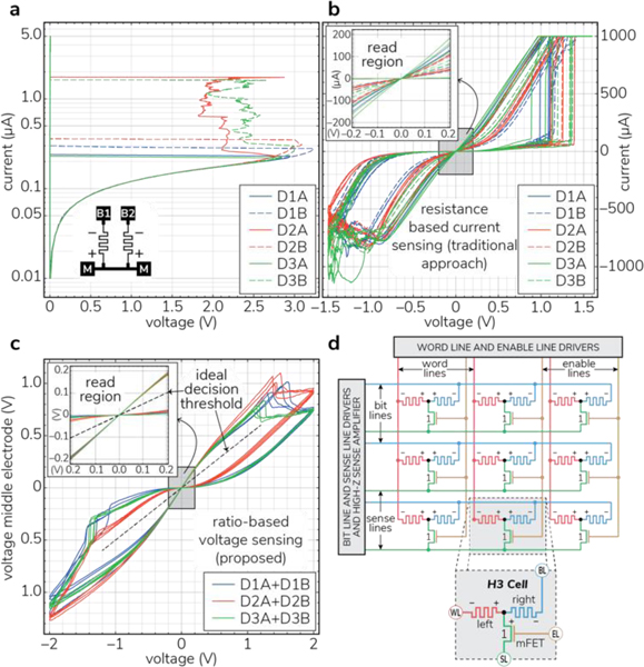
  • [7].Benjamin BV, Gao P, McQuinn E, Choudhary S, Chandrasekaran AR, Bussat J-M, Alvarez-Icaza R, Arthur JV, Merolla PA and Boahen K 2014. Neurogrid: A Mixed-Analog-Digital Multichip System for Large-Scale Neural Simulations Proc. IEEE; 102 699–716 [Google Scholar]
  • [8].Pantazi A, Wozniak S, Tuma T and Eleftheriou E 2016. All-memristive neuromorphic computing with level-tuned neurons Nanotechnology 27 355205 [DOI] [PubMed] [Google Scholar]
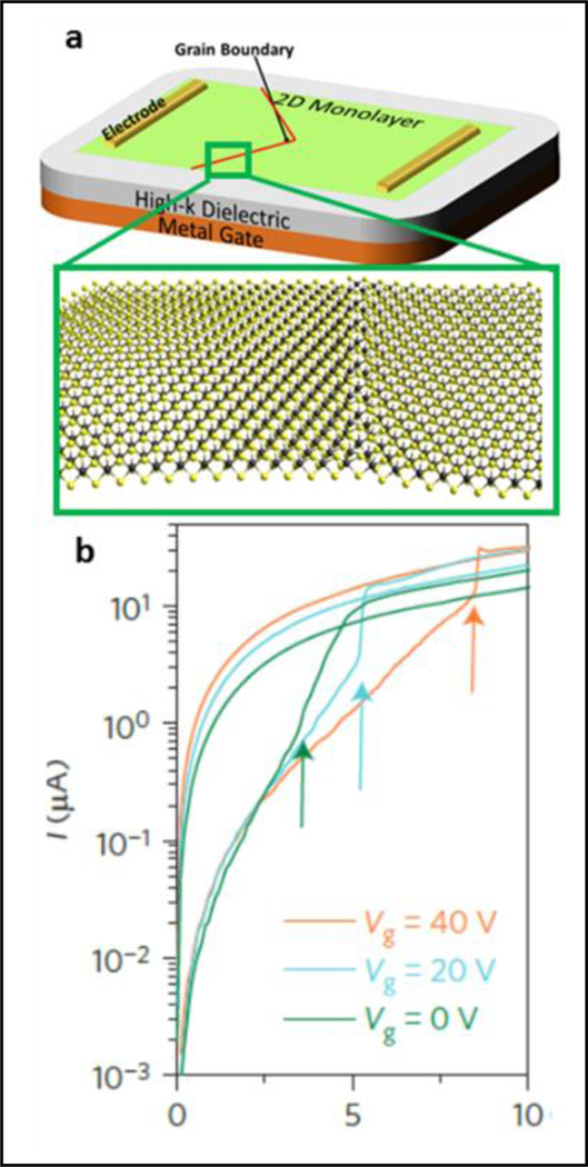
  • [9].Wang Z, Joshi S, Savel’ev S, Song W, Midya R, Li Y, Rao M, Yan P, Asapu S, Zhuo Y, Jiang H, Lin P, Li C, Yoon JH, Upadhyay NK, Zhang J, Hu M, Strachan JP, Barnell M, Wu Q, Wu H, Williams RS, Xia Q and Yang JJ 2018. Fully memristive neural networks for pattern classification with unsupervised learning Nat. Electron. 1 137–45 [Google Scholar]
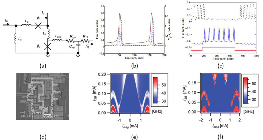
  • [10].Dutta S, Saha A, Panda P, Chakraborty W, Gomez J, Khanna A, Gupta S, Roy K and Datta S 2019. Biologically Plausible Ferroelectric Quasi-Leaky Integrate and Fire Neuron: IEEE) p T140–T1 [Google Scholar]
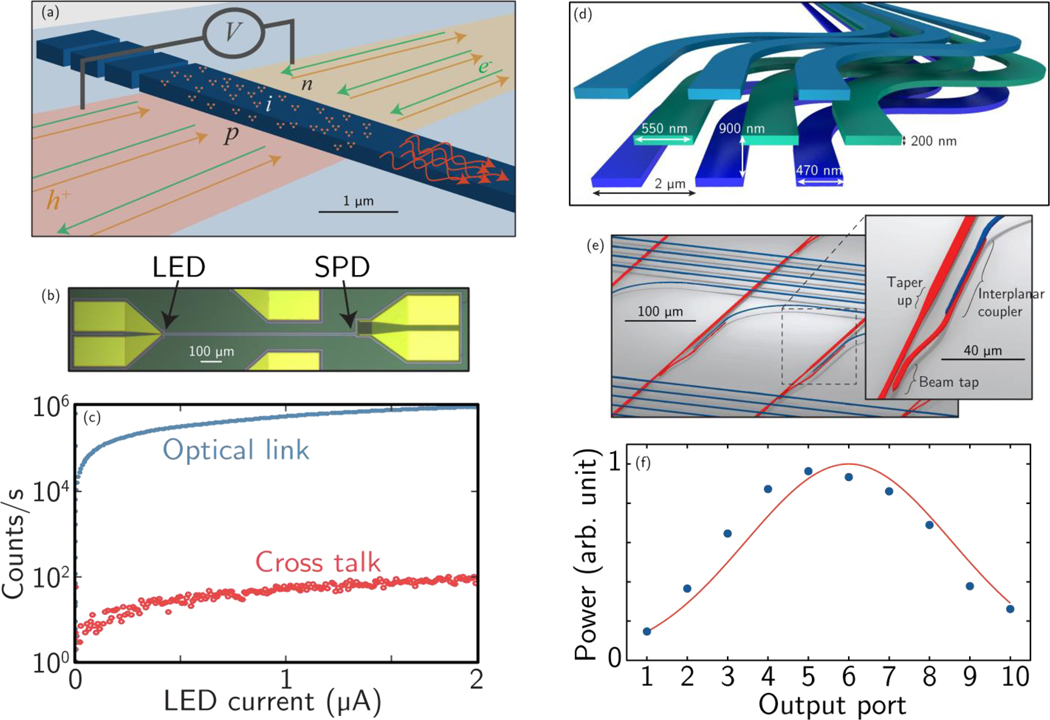
  • [11].Fang Y, Gomez J, Wang Z, Datta S, Khan AI and Raychowdhury A 2019. Neuro-mimetic Dynamics of a Ferroelectric FET Based Spiking Neuron IEEE Elect. Dev. Lett. [Google Scholar]
  • [12].Wijesinghe P, Ankit A, Sengupta A and Roy K 2018. An all-memristor deep spiking neural computing system: A step toward realizing the low-power stochastic brain IEEE Transactions on Emerging Topics in Computational Intelligence 2 345–58 [Google Scholar]
  • [13].Fang Y, Wang Z, Gomez J, Datta S, Khan AI and Raychowdhury A 2019. A Swarm Optimization Solver Based on Ferroelectric Spiking Neural Networks Front. Neurosci. 13 855. [DOI] [PMC free article] [PubMed] [Google Scholar]
  • [14].Kim S, Du C, Sheridan P, Ma W, Choi S and Lu WD 2015. Experimental Demonstration of a Second-Order Memristor and Its Ability to Biorealistically Implement Synaptic Plasticity Nano Lett. 15 2203–11 [DOI] [PubMed] [Google Scholar]
  • [15].Wang Z, Joshi S, Saveliev SE, Jiang H, Midya R, Lin P, Hu M, Ge N, Strachan JP, Li Z, Wu Q, Barnell M, Li G-L, Xin HL, Williams RS, Xia Q and Yang JJ 2017. Memristors with diffusive dynamics as synaptic emulators for neuromorphic computing Nat. Mater 16 101–8 [DOI] [PubMed] [Google Scholar]
  • [16].Pfeiffer M and Pfeil T 2018. Deep Learning With Spiking Neurons: Opportunities and Challenges Front. Neurosci. 12 774. [DOI] [PMC free article] [PubMed] [Google Scholar]
  • [17].Tavanaei A, Ghodrati M, Kheradpisheh SR, Masquelier T and Maida A 2019. Deep learning in spiking neural networks Neural Netw. 111 47–63 [DOI] [PubMed] [Google Scholar]
  • [18].Sengupta A, Ye Y, Wang R, Liu C and Roy K 2019. Going deeper in spiking neural networks: VGG and residual architectures Front. Neurosci. 13 95. [DOI] [PMC free article] [PubMed] [Google Scholar]
  • [19].Bellec G, Scherr F, Hajek E, Salaj D, Legenstein R and Maass W 2019. Biologically inspired alternatives to backpropagation through time for learning in recurrent neural nets arXiv preprint arXiv:1901.09049 [Google Scholar]
  • [20].Du C, Cai F, Zidan MA, Ma W, Lee SH and Lu WD 2017. Reservoir computing using dynamic memristors for temporal information processing Nat. Commun. 8 2204. [DOI] [PMC free article] [PubMed] [Google Scholar]
  • [21].Midya R, Wang Z, Asapu S, Zhang X, Rao M, Song W, Zhuo Y, Upadhyay N, Xia Q, and Yang JJ 2019. Reservoir Computing using Diffusive Memristors, Advanced Intelligent Systems 1, 1900084 [Google Scholar]

RESOURCES