

Abstract
Future multichip packages require Die-to-Die (D2D) interconnects operating at frequencies above 10 GHz; however, the extension of copper interconnects and epoxy dielectrics presents a trade-off between performance and reliability. This paper explores insertion losses and adhesion as a function of interface roughness at frequencies up to 18 GHz. We probe epoxy surface chemistry as a function of curing time and use wet etching to modulate surface roughness. The morphology is quantified by atomic force microscopy (AFM) and two-dimensional fast Fourier transform (2D FFT). Peel test and vector network analysis are used to examine the impacts of both type and level of roughness. The trade-offs between power efficiency and reliability are presented and discussed.
Keywords: Die-to-Die (D2D) interconnects, root mean square (RMS) roughness, spatial frequency, insertion loss, adhesion strength, atomic force microscopy (AFM), two-dimensional fast Fourier transform (2D FFT), x-ray photoelectron spectroscopy (XPS), vector network analysis (VNA), 90°-peel test
I. INTRODUCTION
The growth in artificial intelligence [1–3], terabit ethernet [4–6], internet of things (IoT) [7–10], and autonomous vehicles drive the need for robust, high-performance die-to-die (D2D) interconnects [11–13]. In recent years, several integration methods such as 2.1-D and 2.3-D have been proposed in addition to the more well-known 2.5-D and 3-D approaches. The 2.1-D approach leverages interconnect technology from traditional silicon back end of line (BEOL) processes and allows a relatively low-cost extension of D2D interconnects with fine linewidth and spacing (L/S) [10]. For example, the embedded multi-die interconnect bridge (EMIB) developed at Intel uses a thin silicon bridge with multilayer copper interconnects [1, 14]. The bridges include several interconnect layers with fine (~1 μm) L/S which may be used for signal routing or current redistribution. In addition to bridges with BEOL interconnects, the 2.1-D approach also requires copper redistribution layers and solder pads in organic dielectrics for conventional die-to-bridge chip connections (C2, copper pillar + solder cap). Likewise, the 2.3-D approach extends interconnect density and electrical performance by adding an organic or inorganic interposer. Conventional 2.5-D approaches rely on interposers with passive through-silicon vias (TSV) while 3-D approaches offer the greatest component density and shortest signal paths with vertical stacking. For example, several memory manufacturers recently announced 3D stacks of high bandwidth memory following the HBM3 protocol with data rates over 8 GB/s/IO [10]. New packaging technologies can enable higher D2D bandwidths by either increasing I/O density or increasing I/O speeds (several Gb/s/interconnect) [1].
From a cost and performance perspective, there is considerable interest in extending the use of copper interconnects and organic dielectrics to frequencies >10 GHz [1, 10]. At these frequencies, power efficiency and mechanical reliability can become convoluted, resulting in trade-offs between performance and reliability [15]. For example, increasing the roughness at dielectric-interconnect interfaces was traditionally considered beneficial due to the improved adhesion associated with mechanical interlocking [16]; however, transmission losses due to the skin effect are exacerbated by roughness at high frequencies [17]. Even though interfacial root mean square roughness (RMS roughness) of 200–400 nm improves mechanical adhesion [18, 19], its impact on insertion losses at high frequency (>10 GHz) is not negligible for future multichip packages. Transmission models for typical 10 mm D2D interconnects show that roughness alone can increase insertion losses by as much as 0.3 dB at 10 GHz [17, 20, 21]. This effect can result in a path loss of over 0.5 dB at 20 GHz and exacerbates the stresses caused by higher operating temperatures [17, 22, 23]. Therefore, mitigating power losses while maintaining interface reliability presents a challenge to future copper D2D interconnects with copper and organic dielectric interfaces [20].
The impact of surface roughness on signal loss increases with frequency due to the skin effect [24–26]. Several models have been proposed to account for surface roughness. As shown below, the general form of the Huray Equation in (1) describes the conductor power loss in a textured surface [27]. The Huray model considers the exponential decrease of current density along a path of interconnected copper [27, 28],
| (1) |
where is the power loss of a rough surface, is the power loss of a smooth surface, is an average non-flat Matte area perturbation related to the rough surface, is a flat hexagonal area on a rough surface, is the number of hypothetical copper spheres, is radius of a copper sphere on a rough surface, and is skin depth. As noted by Bok et al., simulation of a 10 mm microstrip using a finite element Huray model showed that a 20 % increase in surface area due to roughness can result in an insertion loss of 0.3–0.4 dB at 10 GHz and an insertion loss of 0.6 dB at 20 GHz [17].
Previous works on copper interconnects have considered the impact of interface roughness on power losses, however they have not explicitly considered the trade-offs with mechanical properties such as adhesion [15, 29–33]. In this report, we explore the mechanical and electrical impacts of smooth and rough epoxy-copper interfaces up to 18 GHz. Wet etching was used to control both the type and level of interface roughness for low-cost manufacturing. The roughness is controlled up to 92 nm RMS roughness to explore smooth interconnects (less than 200 nm RMS roughness of current interconnects [18, 19]) for the future multichip packages. The power efficiency was evaluated using copper transmission lines, and adhesion was evaluated using epoxy substrates including electroless and electrolytic copper films.
II. MATERIALS AND METHODS
Fiber-reinforced epoxy boards (FR-4) were used as substrates. Tetraethyl orthosilicate (TEOS) oxide wafers were obtained from University Wafer Inc., USA. Blend of epoxy (EPON 828, bisphenol-A diglycidyl ether epoxy resin) from Miller-Stephenson Chemicals, methyl-5-norbornene-2,3-dicarboxylic anhydride (NMA), and imidazole were mechanically mixed using a magnetic stir bar for 30 minutes prior to use [34]. The blends of epoxy include 52 % EPON 828, 47 % NMA, and 1 % imidazole. The epoxy blend was spincoated onto an FR-4 substrate using a spin coater (Laurell Technologies Corporation, USA) with a spin speed of 1600 rpm for 90 seconds to yield an 80-μm-thick film. The total curing time of samples in Table II was varied from 1.5 to 3 hours at 150 °C to investigate the impact of curing time on adhesion strength. The impact of curing time was investigated by x-ray photoelectron spectroscopy (XPS) [31, 35]. After the XPS investigation about the impact of curing degree on adhesion strength, the total curing time of 2 hours was applied to epoxy layers of the samples in Table I before the copper deposition, since it has a curing degree higher than 90 % where the glass transition temperature (Tg) of the epoxy is 150 °C. The cyclic ether ring at the ends of epoxide opens and forms an isopropyl segment during the curing as shown in Fig. 1 [36].
TABLE II.
XPS results with different curing time (ranging from 1.5 to 3 hours)
| Curing time (hours) | -OH | C-O-C | C=O |
|---|---|---|---|
| 1.5 | 20.2% | 53.3% | 26.5% |
| 2 | 23.6% | 52.5% | 23.9% |
| 3 | 25.5% | 50.8% | 23.7% |
TABLE I.
CONDITIONS OF WET-CHEMICAL TREATMENTS PROVINDING DIFFERENT RMS ROUGHNESS
| Name | Swell | Etch | RMS Roughness (nm) |
|---|---|---|---|
| Sample A | Not swelled | Not etched | 9 |
| Sample B | (2-(2-butoxyethoxy)ethanol) at 60 °C for 5 minutes | Case 11 for 40 minutes | 25 |
| Sample C | Case 11 for 80 minutes | 35 | |
| Sample D | Case 11 for 120 minutes | 50 | |
| Sample E | (2-(2-butoxyethoxy)ethanol) at 60 °C for 20 minutes | Case 22 for 30 minutes | 92 |
Case 1: 5 % H2SO4 and 5 % H2O2 at 60 °C
Case 2: 30 % H2SO4 and 30 % H2O2 at 60 °C
Fig. 1.

The reaction between diglycidyl ether of biphenyl A (DGEBA, EPON 828) and methyl-5-norbornene-2,3-dicarboxylic anhydride (NMA).
Three types of solutions were used to process epoxy-coated substrates including: a swelling solvent (2-(2-butoxyethoxy)ethanol) at 60 °C, a wet etchant (Case 1: 5 % H2SO4 and 5 % H2O2 at 60 °C, and Case 2: 30 % H2SO4 and 30 % H2O2 at 60 °C for generating higher than 90 nm RMS roughness), and a neutralizing bath (5 % NaOH) at 60 °C to increase the pH and zeta potential of epoxy films [29].
The samples were treated in five different conditions as shown in Table I: Sample A was not swelled and etched, Sample B was swelled for 5 minutes and etched under Case 1 for 40 minutes, Sample C was swelled for 5 minutes and etched under Case 1 for 80 minutes, Sample D was swelled for 5 minutes and etched under Case 1 for 120 minutes, and Sample E was swelled for 20 minutes and etched under Case 2 for 30 minutes.
The surface roughness on the epoxy layer was measured by atomic force microscopy (AFM Model Dimension 3100 AFM, Japan) using an AFM tip with a radius less than 8 nm and a scan rate of 1.0 Hz in tapping mode. The impact of pH on the surface charge of the epoxy surface was measured by the SurPASS electrokinetic analyzer (Anton Paar GmbH, Austria) before the electroless plating.
Following the wet chemical treatments, samples were activated with a PdCl2 and SnCl2 catalyst solution at 60 °C for 30 minutes before electroless copper plating to deposit ~1 μm thick copper layer [37]. The samples were electrolessly coated with copper at 45 °C [38]. The 250 mL of electroless copper plating bath contained 0.03 M CuSO4∙5H2O, 0.05 M ethylenediaminetetraacetic acid (EDTA), 0.5 M KOH, and 0.10 M formaldehyde (pH = 11.5–12.5) with 20 ppm 2,2’-dipyridyl [39].
After the formation of a thin copper layer, copper electroplating was performed with an electrolyte composed of 0.125 M CuSO4 and 0.22 M H2SO4. The copper thickness of 20 μm was used for the insertion loss measurements, and 40 μm thick copper was plated for the 90° peel testing.
Following electroplating, microstrips and adhesion structures were fabricated using traditional lithography and etching. A thin layer of S1813 photoresist was spun onto the samples at 3000 rpm for 45 seconds and baked for 1 minute at 115 °C [40]. The S1813 photoresist was exposed to 365 nm light [41]. Afterward, a 351 developer was applied to the surface of the photoresist. Finally, the samples were etched with 2.45 M CuCl2·2H2O and 6.18 M HCl to create 76.2 mm L × 1 mm W × 20 μm H copper microstrip interconnects as shown in Fig. 2 [42].
Fig. 2.

76.2 mm L × 1mm W × 20 μm H copper transmission line configuration on epoxy dielectric for VNA.
As shown in Fig. 3(a), SMA connectors were soldered onto 76.2 mm L × 1mm W × 20 μm H copper transmission line before a vector network analyzer (VNA, Copper Mountain, USA) was used to measure the s-parameters [43]. Soldered SMA connectors were connected to SMA cables and SMA adapters of the VNA as shown in Fig. 3(b). The s-parameters were measured using S2 VNA software with a wave impedance of 50 Ω [44]. Before the s-parameters were measured, the connectors were de-embedded from the S2 VNA software [45, 46].
Fig. 3.
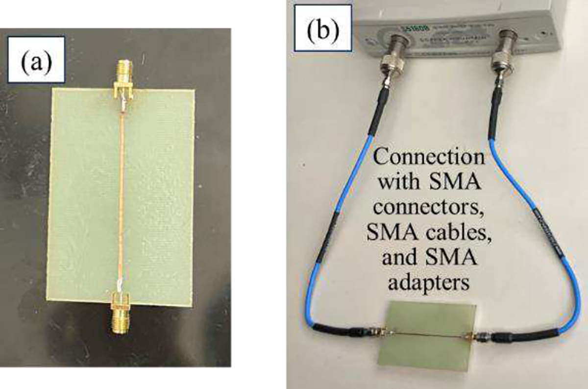
(a) 76.2 mm L × 1mm W × 20 μm H copper transmission line with solder-mounted SMA connectors, (b) Insertion loss measurement set up for VNA (calibrated with automatic calibration module).
The samples for the peel test were prepared by cutting the center with a sharp utility knife to produce a 10 mm wide copper strip as shown in Fig. 4. The 90 ° peel test was conducted at a rate of 25 mm/min based on the procedures described in ASTM B-533 Standard [43].
Fig. 4.

Sample preparation for 90-degree peel test by cutting the center to produce a 10 mm wide copper strip.
III. RESULTS AND DISCUSSION
Results are presented in the following sections: epoxy interfaces, interfacial roughness, adhesion behavior as a function of roughness, and electrical losses as a function of roughness.
A. Chemical and mechanical properties of the epoxy interface
In this section, we investigate the impact of curing and post-cure treatments (swell and etch) on the morphology and the chemical nature of the interface. The chemical interactions at the electroless copper and epoxy interface are complex and depend on the epoxy properties, copper properties, and electroless-catalyst (e.g., Pd-Sn colloids) properties. As noted by Lee et al., metal-polymer adhesion depends on both mechanical (interlocking) and chemical properties at interfaces [44]. Cured epoxies typically have hydroxyl and carboxylate surface groups with interfacial roughness in the range of 2–300 nm [18, 19]. In terms of chemical bonds, which is the strongest mode of adhesion after mechanical interlocking, it is possible to share oxygen atoms in the form of Cu-O-C bonds and Sn-O-C bonds [45, 46]. There are also relatively weaker interactions such as physisorption and chemisorption during the electroless plating [44, 47–49].
The impact of epoxy curing degree on peel strength was investigated by increasing the curing time for epoxy in the absence of adhesion promotors. As shown in Table II and Fig. 5, the peel strength increases with curing time, which is mainly ascribed to the increase in hydrophilic hydroxyl (OH) groups at the epoxy surface. Table II shows the composition of OH groups increases from 20.2 % to 25.5 % with the curing time increasing from 1.5 hours to 3 hours, while the composition of C-O-C groups decreases. Further, subsequent wet alkaline treatments before seeding also improve the surface charge of the dielectric by changing hydrophilicity. The surface zeta potential as a function of pH is shown in Fig. 6. The surface zeta potential decreases from 0.02 V to −0.08 V with the pH increasing from 3 to 10. The epoxy surface shows an isoelectric point at a pH of 3.5. The high concentration of surface hydroxyl groups created by curing and post-cure alkaline treatments is thought to improve the seeding process (for electroless copper deposition) and improve chemical interactions between the dielectric and metal.
Fig. 5.

Peel strength of the copper on the epoxy layer after 1.5, 2, and 3 hours curing time.
Fig. 6.

Relationship between pH ranging from 3 to 10 and zeta potential of the epoxy resin.
B. Interfacial Roughness
As described by Hayden et al., [29] it is important to differentiate the surface morphology of the dielectric by roughness type viz., “peak-valley” roughness and “pore-type” roughness. As shown in Fig. 7, peak valley roughness refers to higher spatial frequency with relatively shallow variations while pore-type roughness is observed at lower spatial frequencies with relatively deeper pores. Here, we quantify roughness type using AFM and 2D FFT. The FFT has been used by Kumar et al. and Patrikar et al. to show the impact of roughness modes on the performance of interconnects [50–52].
Fig. 7.

5 μm × 5 μm AFM images of the epoxy surface (a) Sample A (9 nm RMS roughness), (b) Sample B (25 nm RMS roughness), (c) Sample C (35 nm RMS roughness), (d) Sample D (50 nm RMS roughness), and (e) Sample E (92 nm RMS roughness).
Table I and Fig. 8 show the RMS roughness of the epoxy surface (measured by AFM) as a function of etching time. The surface RMS roughness increases from 9 nm (Sample A) to 50 nm (Sample D) RMS roughness after 120 minutes of acid etch treatment. More specifically, as shown in Table I and Fig. 7, the type of roughness also depends on etching times. In this case, the epoxy surface first develops a relatively uniform (i.e., higher spatial frequency, lower RMS roughness) “peak-valley” type roughness until 80 minutes of acid etch treatment producing RMS roughness of 35 nm (Sample C). With longer (Sample D) and more aggressive (Sample E) etching, more non-uniform “pore-type” roughness is observed (with underlying peak-valley roughness). The deep pores associated with pore-type roughness support mechanical interlocking [29].
Fig. 8.

Roughness development with different etch treatment times (ranging from 0 to 120 minutes) following a 5-minute swell treatment using (2-(2-butoxyethoxy)ethanol) at 60 °C for the EPON 828/NMA mixture. Etching solution included 5 % H2SO4 and 5 % H2O2 at 60 °C.
Fig. 10 shows the log (normalized intensity) of roughness at different spatial frequencies based on 2D FFT analyses in Fig. 9(a)-(e). The different spatial frequencies can be used to categorize roughness types (peak-valley roughness or pore-type roughness). In Fig. 10, we define “SF−3” as the spatial frequency at a normalized intensity of 10−3. In this case, the pore-type roughness ((d) and (e) in Fig. 7) has relatively low SF−3 values (approximately 0 to 15 μm−1), while the peak-valley roughness ((a), (b) and (c) in Fig. 7) has higher SF−3 values (approximately 15 to 25 μm−1). This comparison of spatial frequency provides a more quantitative way to describe the type of roughness.
Fig. 10.

log (normalized intensity) after 2D FFT of 5 μm × 5 μm AFM images from Fig. 7 using Gwyddion software as a function of spatial frequency from 0 to 25 μm−1. Y-axis indicates log (normalized intensity), where intensity refers to the intensity of spatial frequency in Fig. 9. X-axis corresponds to spatial frequency on the linecut in Fig. 9.
Fig. 9.

Two-dimensional Fast Fourier Transform of 5 μm × 5 μm AFM images from Fig. 7 following different RMS roughness of (a) 9 nm, (b) 25 nm, (c) 35 nm, and (d) 50 nm and (e) 92 nm. X-axes and Y-axes denote spatial frequency. Color legends correspond to intensity of spatial frequency. Insets represent conceptional cross-sectional sketches capturing the modes of roughness (peak-valley roughness versus pore-type roughness).
C. Interfacial Roughness and adhesion
As shown in Fig. 11, the peel strength depends on both the RMS roughness and the type of roughness. With regard to the peak valley roughness, the peel strength increases to 20 N/m at an RMS roughness of 35 nm in Fig. 11(a). In this domain, peak-valley roughness dominates, and adhesion is thought to increase due to the larger interfacial area resulting in an increased density of chemical and electrostatic interactions [16, 47, 48, 53]. When the morphology includes a greater degree of pore-type roughness, the peel strength increases by a factor of 1.8 (21 N/m at 50 nm RMS to 37 N/m at 92 nm RMS). The deep pores are thought to improve adhesion via mechanical interlocking [29, 54]. As shown in Fig. 11(b), the transition of adhesion strength as a function of roughness type is more evident when plotting the peel strength versus the SF−3. In this plot, there are clearly two domains associated with different adhesion mechanisms.
Fig. 11.

(a) Relationship between peel strength of the copper on the epoxy layer and interfacial RMS roughness (ranging from 9 to 92 nm), (b) Relationship between peel strength of the copper on the epoxy layer and SF−3. RMS roughness of each of the data points are labeled. Rrms represents RMS roughness.
D. Interfacial Roughness and Insertion Loss
Fig. 12 illustrates the effect of conductor roughness and the skin effect at high frequencies. For example, at a frequency of 10 GHz, the additional loss solely due to added roughness (from 9 nm (Sample A) to 92 nm (Sample E)) is 0.17 dB/mm. The additional losses due to roughness continue to grow at higher frequencies. At 18 GHz, the insertion loss due to roughness grows to 0.19 dB/mm, which is 12 % higher than the value at 10 GHz. Rough interfaces lead to absorption and scattering of electromagnetic waves resulting in power loss [27].
Fig. 12.

The impact of interfacial roughness (ranging from 9 to 92 nm RMS roughness) on insertion loss as a function of frequency. Rrms represents RMS roughness.
Fig. 13 presents the insertion losses as a function of RMS roughness and spatial frequency. The insertion loss at 18 GHz linearly decreases as SF−3 increases in Fig. 13(b). The linear nature of the relationship suggests that the same mechanisms, specifically absorption and scattering of electromagnetic waves at rough interfaces, are responsible for the losses across these spatial frequencies. In this case, the pore-type roughness shows a maximum insertion loss of 0.39 dB/mm at SF−3 of 5 μm−1 (primarily pore type) which is nearly twice the insertion loss of 0.20 dB/mm of a smooth surface (SF−3 of 24 μm−1).
Fig. 13.

(a) Nonlinear relationship between surface roughness (ranging from 9 to 92 nm RMS roughness) and insertion loss at 18 GHz, (b) Linear relationship between SF−3 (R2=0.9952) and insertion loss at 18 GHz. RMS roughness of each of the data points are labeled. Rrms represents RMS roughness.
In general, power losses increase as the interface roughness increases [27, 28, 55]. The impact of power efficiency () for a typical 5 mm Cu D2D interconnect may be modeled using Equation (2) [56]. Fig. 14 shows that power efficiency decreased by 9 % at 1 GHz due to the increase in RMS roughness (from 9 nm (Sample A) to 92 nm (Sample E)). At 18 GHz, power efficiency decreased by 16 %, which is 78 % larger than the value at 1 GHz. Rough interfaces have stronger impact on scattering of electromagnetic waves at higher frequencies lowering power efficiency [27]. It is interesting to note the nonlinear relationship between power efficiency and RMS roughness. In this study, an increase in the RMS roughness from 9 nm to 35 nm (peak-valley roughness) led to a 5% decrease in power efficiency; however, the increase in roughness from 35 nm to 92 nm (transition to pore-type roughness) caused an 11% decrease in power efficiency [57].
Fig. 14.

The impact of interfacial roughness (ranging from 9 to 92 nm RMS roughness) on power efficiency of a 5 mm copper transmission line on the epoxy layer.
| (2) |
Fig. 15 shows the trade-off between the power efficiency and adhesion strength as a function of roughness. Over this range of roughness, power efficiency decreases by 16 %, while the peel strength increases by a factor of 6.
Fig. 15.

Tradeoffs between power efficiency at 18 GHz and peel strength as a function of RMS roughness ranging from 9 to 92 nm.
IV. CONCLUSIONS
These results indicate that the extension of copper interconnects and polymer dielectrics to multi-GHz frequencies may be limited by the trade-off of mechanical reliability and electrical performance. Smooth interconnect-dielectric interfaces are critical for mitigating losses due to the skin effect in these frequency ranges, however, the absence of mechanical anchoring via interlocking results in relatively weak adhesion that can lead to delamination and mechanical failure. In the case of epoxy dielectrics, curing and alkaline wet treatments add hydroxyl groups and improve the adhesion to smooth copper; however, in the absence of mechanical interlocking, the adhesion strength is relatively low. This indicates that adhesion promoters or interlayers are needed to enable reversible expansion and contraction without delamination.
ACKNOWLEDGMENT
This work is supported in part by Semiconductor Research Corporation (SRC) under grant PKG 3074.001. S. Park acknowledges the National Institutes of Health for financial support (NIBIB P41-EB020594).
Footnotes
Color versions of one or more of the figures in this article are available online at http://ieeexplore.ieee.org.
Contributor Information
Junghyun Park, Gordon A. and Mary Cain Department of Chemical Engineering, Louisiana State University, Baton Rouge, LA 70803 USA.
Jiayou Xu, Gordon A. and Mary Cain Department of Chemical Engineering, Louisiana State University, Baton Rouge, LA 70803 USA.
Anthony Engler, Gordon A. and Mary Cain Department of Chemical Engineering, Louisiana State University, Baton Rouge, LA 70803 USA.
Jaimal Williamson, Texas Instruments Incorporated, Dallas, TX 75243 USA.
Varughese Mathew, NXP Semiconductors, Austin, TX 78735 USA.
Sunggook Park, Mechanical & Industrial Engineering Department and Center for Bio-Modular Multiscale Systems, Louisiana State University, Baton Rouge, LA 70803 USA.
John Flake, Gordon A. and Mary Cain Department of Chemical Engineering, Louisiana State University, Baton Rouge, LA 70803 USA.
REFERENCES
- [1].Mahajan R, Qian Z, Viswanath RS, Srinivasan S, Aygün K, Jen W-L, Sharan S, and Dhall A, “Embedded multidie interconnect bridge—A localized, high-density multichip packaging interconnect,” IEEE transactions on components, packaging and manufacturing technology, vol. 9, no. 10, pp. 1952–1962, 2019. [Google Scholar]
- [2].Loh GH, Jerger NE, Kannan A, and Eckert Y, “Interconnect-memory challenges for multi-chip, silicon interposer systems.” pp. 3–10. [Google Scholar]
- [3].Ravichandran S, Yamada S, Park G, Chen H-W, Shi T, Buch C, Liu F, Smet V, Sundaram V, and Tummala R, “2.5 D glass panel embedded (GPE) packages with better I/O density, performance, cost and reliability than current silicon interposers and high-density fan-out packages.” pp. 625–630. [Google Scholar]
- [4].Bernabe S, Wilmart Q, Hasharoni K, Hassan K, Thonnart Y, Tissier P, Desieres Y, Olivier S, Tekin T, and Szelag B, “Silicon photonics for terabit/s communication in data centers and exascale computers,” Solid-State Electronics, vol. 179, pp. 107928, 2021. [Google Scholar]
- [5].Jain P, “Recent trends in next generation terabit Ethernet and gigabit wireless local area network.” pp. 106–110. [Google Scholar]
- [6].Holloway JW, Dogiamis GC, and Han R, “Innovations in terahertz interconnects: High-speed data transport over fully electrical terahertz waveguide links,” IEEE Microwave Magazine, vol. 21, no. 1, pp. 35–50, 2019. [Google Scholar]
- [7].He X, Tehrani BK, Bahr R, Su W, and Tentzeris MM, “Additively manufactured mm-wave multichip modules with fully printed “smart” encapsulation structures,” IEEE Transactions on Microwave Theory and Techniques, vol. 68, no. 7, pp. 2716–2724, 2019. [Google Scholar]
- [8].Martins A, Pinheiro M, Ferreira AF, Almeida R, Matos F, Oliveira J, Silva RP, Santos H, Monteiro M, and Gamboa H, “Heterogeneous integration challenges within wafer level fan-out SiP for wearables and IoT.” pp. 1485–1492. [Google Scholar]
- [9].Lee HJ, Mahajan R, Sheikh F, Nagisetty R, and Deo M, “Multi-die Integration Using Advanced Packaging Technologies.” pp. 1–7. [Google Scholar]
- [10].Lau JH, “Recent Advances and Trends in Advanced Packaging,” IEEE Transactions on Components, Packaging and Manufacturing Technology, vol. 12, no. 2, pp. 228–252, 2022. [Google Scholar]
- [11].Wesling P, “The Heterogeneous integration roadmap: Enabling technology for systems of the future.” pp. 1–4. [Google Scholar]
- [12].Kim D-W, Au K, Luo HYLX, Ye YL, Bhattacharya S, and Lo GQ, “2.5 D silicon optical interposer for 400 Gbps electronic-photonic integrated circuit platform packaging.” pp. 1–4. [Google Scholar]
- [13].Shao YS, Clemons J, Venkatesan R, Zimmer B, Fojtik M, Jiang N, Keller B, Klinefelter A, Pinckney N, and Raina P, “Simba: Scaling deep-learning inference with multi-chip-module-based architecture.” pp. 14–27. [Google Scholar]
- [14].Mahajan R, Sankman R, Patel N, Kim D-W, Aygun K, Qian Z, Mekonnen Y, Salama I, Sharan S, and Iyengar D, “Embedded multi-die interconnect bridge (EMIB)--a high density, high bandwidth packaging interconnect.” pp. 557–565. [Google Scholar]
- [15].Cheah BE, Lo HL, and Kong J, “Study of dielectric material property impact on insertion loss for advanced packaging solutions.” pp. 134–135. [Google Scholar]
- [16].Schaubroeck D, Mader L, Dubruel P, and Vanfleteren J, “Surface modification of an epoxy resin with polyamines and polydopamine: Adhesion toward electroless deposited copper,” Applied Surface Science, vol. 353, pp. 238–244, 2015/10/30/, 2015. [Google Scholar]
- [17].Lo HL, and Cheah BE, “Study of conductor surface roughness impact on package insertion loss.” pp. 1–4. [Google Scholar]
- [18].Wang C, Ji X, Roy A, Silberschmidt VV, and Chen Z, “Shear strength and fracture toughness of carbon fibre/epoxy interface: effect of surface treatment,” Materials & Design, vol. 85, pp. 800–807, 2015. [Google Scholar]
- [19].Hayden HT, Enhanced adhesion between electroless copper and advanced substrates: Georgia Institute of Technology, 2008. [Google Scholar]
- [20].Guo J, Liang GS, and Liu X, “Frequency-dependent transmission line fractional model and its solution based on skin effect.” pp. 1208–1211. [Google Scholar]
- [21].Gold G, and Helmreich K, “A physical surface roughness model and its applications,” IEEE Transactions on Microwave Theory and Techniques, vol. 65, no. 10, pp. 3720–3732, 2017. [Google Scholar]
- [22].Casper BK, Haycock M, and Mooney R, “An accurate and efficient analysis method for multi-Gb/s chip-to-chip signaling schemes.” pp. 54–57. [Google Scholar]
- [23].Yu B, Liu Y, Ye Y, Ren J, Liu X, and Gu QJ, “High-Efficiency Micromachined Sub-THz Channels for Low-Cost Interconnect for Planar Integrated Circuits,” IEEE Transactions on Microwave Theory and Techniques, vol. 64, no. 1, pp. 96–105, 2016. [Google Scholar]
- [24].Spencer TJ, Saha R, Chen J, Bashirullah R, and Kohl PA, “Air cavity transmission lines for off-chip interconnects characterized to 40 GHz,” IEEE Transactions on Components, Packaging and Manufacturing Technology, vol. 2, no. 3, pp. 367–374, 2012. [Google Scholar]
- [25].Park S, Materials, processes, and characterization of extended air-gaps for the intra-level interconnection of integrated circuits: Georgia Institute of Technology, 2008. [Google Scholar]
- [26].Triverio P, Grivet-Talocia S, Nakhla MS, Canavero FG, and Achar R, “Stability, causality, and passivity in electrical interconnect models,” IEEE Transactions on Advanced Packaging, vol. 30, no. 4, pp. 795–808, 2007. [Google Scholar]
- [27].Huray PG, Oluwafemi O, Loyer J, Bogatin E, and Ye X, “Impact of copper surface texture on loss: A model that works,” DesignCon 2010, vol. 1, pp. 462–483, 2010. [Google Scholar]
- [28].Huray OOPG, Loyer J, Bogatin E, “Impact of Copper Surface Texture on Loss: A Model that Works,” in DesignCon 2010, 2010. [Google Scholar]
- [29].Hayden H, Elce E, Allen SAB, and Kohl PA, “Adhesion enhancement between electroless copper and epoxy-based dielectrics,” IEEE Transactions on Advanced Packaging, vol. 32, no. 4, pp. 758–767, 2009. [Google Scholar]
- [30].Siau S, Vervaet A, Schacht E, Degrande S, Callewaert K, and Van Calster A, “Chemical modification of buildup epoxy surfaces for altering the adhesion of electrochemically deposited copper,” Journal of the Electrochemical Society, vol. 152, no. 9, pp. D136, 2005. [Google Scholar]
- [31].Granado L, Kempa S, Gregoriades LJ, Brüning F, Bernhard T, Flaud V, Anglaret E, and Fréty N, “Improvements of the Epoxy–Copper Adhesion for Microelectronic Applications,” ACS Applied Electronic Materials, vol. 1, no. 8, pp. 1498–1505, 2019/08/27, 2019. [Google Scholar]
- [32].Bok S, Lim G-H, and Lim B, “UV/ozone treatment for adhesion improvement of copper/epoxy interface,” Journal of Industrial and Engineering Chemistry, vol. 46, pp. 199–202, 2017/02/25/, 2017. [Google Scholar]
- [33].Horn III AF, Reynolds JW, LaFrance PA, and Rautio JC, “Effect of conductor profile on the insertion loss, phase constant, and dispersion in thin high frequency transmission lines.” pp. 1–22. [Google Scholar]
- [34].Dias Filho NL, H. A. d. Aquino, G. Pires, and L. Caetano, “Relationship between the dielectric and mechanical properties and the ratio of epoxy resin to hardener of the hybrid thermosetting polymers,” Journal of the Brazilian Chemical Society, vol. 17, pp. 533–541, 2006. [Google Scholar]
- [35].Siau S, Roo B, and Vervaet A, XPS-study of Cu/epoxy Interfaces after different Wet Chemical Treatments, 2007. [Google Scholar]
- [36].Couture G, Granado L, Fanget F, Boutevin B, and Caillol S, “Limonene-based epoxy: Anhydride thermoset reaction study,” Molecules, vol. 23, no. 11, pp. 2739, 2018. [DOI] [PMC free article] [PubMed] [Google Scholar]
- [37].Chen M-S, Brandow SL, and Dressick WJ, “Additive channel-constrained metallization of high-resolution features,” Thin Solid Films, vol. 379, no. 1–2, pp. 203–212, 2000. [Google Scholar]
- [38].Dixit NK, Srivastava R, and Narain R, “Improving surface roughness of the 3D printed part using electroless plating,” Proceedings of the Institution of Mechanical Engineers, Part L: Journal of Materials: Design and Applications, vol. 233, no. 5, pp. 942954, 2019. [Google Scholar]
- [39].Park KJ, Lim T, Kim MJ, Kim KH, Hwang S-M, and Kim JJ, “In-situ transmittance measurement for characterization of organic additives in Cu electroless deposition,” Journal of Electroanalytical Chemistry, vol. 731, pp. 157–162, 2014/10/01/, 2014. [Google Scholar]
- [40].Zhang F-Y, Prasad AK, and Advani SG, “Investigation of a copper etching technique to fabricate metallic gas diffusion media,” Journal of Micromechanics and Microengineering, vol. 16, no. 11, pp. N23, 2006. [Google Scholar]
- [41].Rathsack BM, Photoresist modeling for 365 nm and 257 nm laser photomask lithography and multianalyte biosensors indexed through shape recognition: The University of Texas at Austin, 2001. [Google Scholar]
- [42].Cakir O, “Copper etching with cupric chloride and regeneration of waste etchant,” Journal of Materials Processing Technology, vol. 175, no. 1, pp. 63–68, 2006/06/01/, 2006. [Google Scholar]
- [43].“ASTM B Standard 533–85, 2002.” [Google Scholar]
- [44].Lee L-H, Fundamentals of adhesion: Springer Science & Business Media, 2013. [Google Scholar]
- [45].Duguet T, Gavrielides A, Esvan J, Mineva T, and Lacaze-Dufaure C, “DFT Simulation of XPS Reveals Cu/Epoxy Polymer Interfacial Bonding,” The Journal of Physical Chemistry C, vol. 123, no. 51, pp. 30917–30925, 2019/12/26, 2019. [Google Scholar]
- [46].Khdary NH, El Enany G, Almalki AS, Alhassan AM, Altamimi A, and Alshihri S, “Preparation of Cu/Sn-Organic Nano-Composite Catalysts for Potential Use in Hydrogen Evolution Reaction and Electrochemical Characterization,” Nanomaterials, vol. 13, no. 5, pp. 911, 2023. [DOI] [PMC free article] [PubMed] [Google Scholar]
- [47].Ge J, Turunen M, and Kivilahti J, “Surface modification and characterization of photodefinable epoxy/copper systems,” Thin Solid Films, vol. 440, no. 1–2, pp. 198–207, 2003. [Google Scholar]
- [48].Schaubroeck D, Van den Eeckhout E, De Baets J, Dubruel P, Vaeck L, and Calster A, “Surface Modification of a Photo-Definable Epoxy Resin with Polydopamine to Improve Adhesion with Electroless Deposited Copper,” Journal of Adhesion Science and Technology - J ADHES SCI TECHNOL, vol. 26, pp. 1–14, 10/01, 2012. [Google Scholar]
- [49].C. A. Hunter, and J. K. Sanders, “The nature of. pi.−. pi. interactions,” Journal of the American Chemical Society, vol. 112, no. 14, pp. 5525–5534, 1990. [Google Scholar]
- [50].Kumar S, and Sharma R, “Chip-to-Chip Copper Interconnects With Rough Surfaces: Analytical Models for Parameter Extraction and Performance Evaluation,” IEEE Transactions on Components, Packaging and Manufacturing Technology, vol. 8, no. 2, pp. 286–299, 2018. [Google Scholar]
- [51].Patrikar RM, Dong CY, and Zhuang W, “Modelling interconnects with surface roughness,” Microelectronics Journal, vol. 33, no. 11, pp. 929–934, 2002/11/01/, 2002. [Google Scholar]
- [52].Patrikar RM, “Modeling and simulation of surface roughness,” Applied Surface Science, vol. 228, no. 1, pp. 213–220, 2004/04/30/, 2004. [Google Scholar]
- [53].Siau S, Vervaet A, Schacht E, Demeter U, and Van Calster A, “Epoxy polymer surface modification through wet-chemical organic surface synthesis for adhesion improvement in microelectronics,” Thin Solid Films, vol. 495, no. 1–2, pp. 348–356, 2006. [Google Scholar]
- [54].Gent A, and Lin C-W, “Model studies of the effect of surface roughness and mechanical interlocking on adhesion,” The Journal of Adhesion, vol. 32, no. 2–3, pp. 113–125, 1990. [Google Scholar]
- [55].Hammerstad E, and Jensen O, “Accurate Models for Microstrip Computer-Aided Design.” pp. 407–409. [Google Scholar]
- [56].Instruments N, “The guide to selecting an rf switch,” white paper, 2014. [Google Scholar]
- [57].Beatty RW, “Insertion loss concepts,” Proceedings of the IEEE, vol. 52, no. 6, pp. 663–671, 1964. [Google Scholar]