Abstract
Fluorescent nanodiamonds (FNDs) with nitrogen-vacancy centers are pivotal for advancing quantum photonics and imaging through deterministic quantum state manipulation. However, deterministic integration of quantum emitters into photonic devices remains a challenge due to the need for high coupling efficiency and Purcell enhancement. We report a deterministic FND-integrated nanofocusing device achieved by assembling FNDs at a plasmonic waveguide tip through plasmonic-enhanced optical trapping. This technique not only increases the emission rate by 58.6 times compared to isolated FNDs but also preferentially directs radiation into the waveguide at a rate 5.3 times higher than that into free space, achieving an exceptional figure-of-merit of ∼3000 for efficient energy transfer. Our findings represent a significant step toward deterministic integration in quantum imaging and communication, opening new avenues for quantum technology advancements.
Keywords: fluorescent nanodiamond, plasmonic optical trapping, plasmonic coupling, silver nanowire
Quantum emitters, particularly nitrogen-vacancy (NV) centers in fluorescent nanodiamonds (FNDs), have emerged as pivotal components in advancing quantum information and imaging technologies due to their remarkable quantum efficiency, precise state control, and resilience against photobleaching and photoblinking. These emitters are increasingly recognized for their potential in applications ranging from super-resolution imaging1−3 to molecular tracking4−6 and broader quantum-related fields.7,8 Traditional setups involving these quantum emitters have relied on bulky optical configurations, prompting a pressing demand for their integration into more compact and efficient photonic structures.
Recent advancements have focused on merging FNDs with plasmonic architectures to leverage the enhancement effects offered by surface plasmon polaritons (SPPs). This integration is crucial for amplifying optical absorption, boosting emission rates, and enhancing the collection efficiency. Efforts to position FNDs accurately within these metallic nanostructures have employed a variety of techniques including self-assembly,9,10 double-patterning e-beam lithography,11 atomic force microscopy,12−16 and optical trapping within nanocavities.17 Building on these developments, our approach emphasizes deterministic integration of FNDs onto high-plasmonic-enhancement sites of a plasmonic waveguide. This strategy not only ensures precise alignment with SPP modes but also optimizes the interaction between the quantum emitters and the plasmonic environment, substantially increasing the system’s overall optical performance.
Crucially, three primary energy dissipation channels—direct free-space radiation, SPP generation, and nonradiative damping—define the efficiency of a quantum emitter within a plasmonic system. Of these, enhancing the SPP generation channel is pivotal for maximizing plasmonic utility. This enhancement is dependent on three factors: the Purcell factor FP, which quantifies spontaneous emission enhancement; the coupling efficiency between the quantum emitter and the SPP mode; and the damping rate, which is influenced by the propagation length of the SPPs. The product of these factors, normalized by the working wavelength, serves as an figure of merit (FOM) to assess the capacity for efficient long-range energy transfer. Among various plasmonic materials, silver nanowires (AgNWs) stand out due to their superior plasmonic properties and are particularly well-suited for quantum applications. The bicrystalline AgNWs have atomically smooth surfaces, making them an excellent choice for sustaining a long-range SPP with minimal loss. The unique geometry of AgNWs allows for tight field confinement and a high degree of light–matter interaction,18,19 which is crucial for enhancing the performance of quantum emitters like FNDs.
In this study, we harness the principle of plasmonic nanofocusing to realize the deterministic assembly of FNDs at the tip of a AgNW. The core mechanism centers on directing incident light through an optical fiber to the apex of a AgNW, forming a plasmonic hot spot where the electric field intensities are strategically concentrated. This hot spot is critical, as it represents the location where the plasmonic trapping force is maximized due to the peak electric fields. Moreover, this location also achieves a maximal plasmonic enhancement of quantum emissions and optimizes the coupling efficiency of radiation from the quantum emitters into the SPP mode of the waveguide. We employ a time-resolved localization technique to meticulously trace and analyze the trapping dynamics, providing a detailed view of the interactions of quantum emitters with the plasmonic traps. The findings from our analysis reveal that the quantum yield for SPP generation in this FND-AgNW system exceeds 35%, signifying that a substantial portion of the radiation is effectively captured and utilized by the nanofocusing probe. This efficient engagement of quantum emissions at the plasmonic hot spots is instrumental for advancing hybrid quantum sensing systems, enhancing both their sensitivity and resolution.
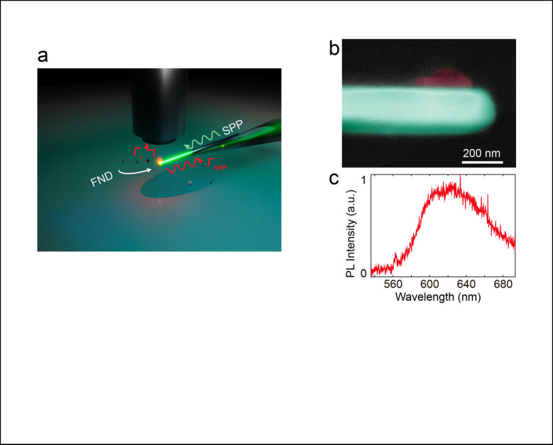
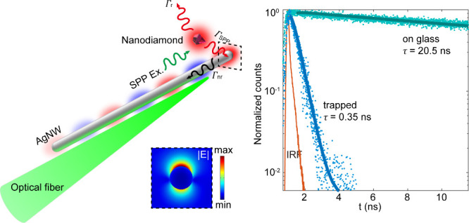
The high-external-efficiency nanofocusing technique is pivotal to our method, integrating plasmonic trapping, optical excitation, and efficient quantum signal collection. As depicted in Figure 1a, incident light is funneled through a tapered optical fiber, exciting tightly confined SPPs on the AgNW. This assembly is housed within a fluidic channel beneath an upright optical microscope, which allows for detailed analysis of particle dynamics in the plasmonic trap. A solution containing FNDs, with an average size of ∼40 nm, is introduced into the channel, and imaging is performed to precisely localize these particles. The scanning electron microscopy (SEM) image in Figure 1b, enhanced with false color for better visibility, shows an FND particle optimally positioned near the tip of the AgNW. Figure 1c displays the photoluminescence spectrum, illustrating the typical emission characteristics observed during these experiments.
Figure 1.
Plasmonic trapping for quantum emitters. (a) Schematic of the AgNW-fiber nanofocusing probe for plasmonic trapping of NV-FNDs at the probe tip. The FND has radiative channels into the free space (decay rate Γr) and the SPP waveguide (decay rate ΓSPP). The bottom panel shows the tightly confined SPP. (b) False-colored SEM image of the AgNW (green) and trapped FND (red). (c) A representative PL spectrum from a trapped FND, measured through the free-space radiation channel.
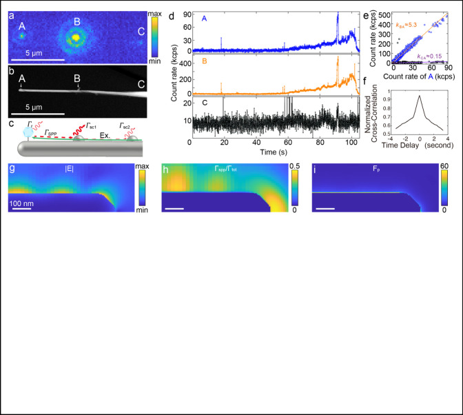
When an FND approaches the AgNW tip, it is illuminated by the evanescent field of the SPP, resulting in emission predominantly through two primary channels: direct free space radiation (decay rate Γr) and the SPP channel (decay rate ΓSPP). Variations in the direct radiation rate during the trapping process are recorded by monitoring the PL intensity from the trapping side with a camera. To accurately gauge the radiation rate into the SPP channel, nanoparticles are strategically attached to the AgNW waveguide as scatterers, identified as B and C in Figure 2a. The SEM image in Figure 2b confirms the presence of both the trapped FND particle and the scatterer at points A and B, respectively. The temporal fluorescence intensity profiles of spots A, B, and C throughout the trapping period of a typical FND are illustrated in Figure 2d. The FND particle approaches the SPP trapping spot A approximately 60 s into the experiment, as evidenced by a rise in fluorescent intensity at both sites A and B. Subsequently, a significant spike in fluorescent intensity is observed around the 90 s mark, likely due to the alignment of the FND dipole with the evanescent electric field during its random Brownian motion. This spike is followed by a marked decrease in fluorescent intensity, due to the plasmonic quenching as the dipole–metal distance diminishes to below 10 nm.
Figure 2.
Observation of the nanoparticle trapping by the plasmonic probe. (a) Representative wide-field PL image extracted from video footage showcasing an FND trapped at site A on a AgNW probe. Particles at sites B and C on the AgNW surface facilitate the coupling of SPPs into free space. (b) The SEM image validates the presence of the nanostructures at the specified locations. (c) Schematic representation of the energy transfer pathways within the FND-AgNW assembly. (d) Temporal fluorescence intensity profiles for PL emission from the three distinct locations. (e) Analysis of PL intensity correlations between the different spots. (f) Normalized cross-correlation of events from sites A and B. (g) Distribution of the electric field of the HE1 mode SPP introduced into the AgNW from the left port. (h) Visualization of SPP mode coupling efficiency from a quantum emitter, derived from the positional mapping of an electrical dipole emitter. (i) Spatial representation of the Purcell factor (Fp) for a dipole emitter at varying proximities.
Correlation analysis on the fluorescent intensities shown in Figure 2d demonstrates a high Pearson correlation coefficient of 0.95 between sites A and B, which is calculated using the following formula:
| 1 |
Here Ai and Bi are the individual intensity measurements for site A and B, and A̅ and B̅ are the average intensities. This substantial correlation underscores that emissions from both sites originate from a single FND, indicating synchronized fluorescence behavior due to a shared quantum event.
Cross-correlation is a measure of the similarity between two waveforms as a function of a time delay applied to one of them. This is especially useful in the context of time series analysis or signal processing to evaluate their correlations. Mathematically, the cross-correlation follows
| 2 |
where τ varies over the desired range of lags.
Figure 2f displays the cross-correlation between the two luminescent spots in Figure 2, over a range of time delays. The peak at zero lag indicates a high degree of correlation (near unity) between the two sites, suggesting that the fluctuations in the light intensity at both spots are synchronized and likely emanate from the same light source. The symmetrical shape of the curve around the zero delay further reinforces this interpretation, as it demonstrates that the temporal alignment of the signals maximizes their correlation, typical of signals sharing a common origin. This strong correlation supports the hypothesis that the observed emissions at both sites are manifestations of the same quantum events within the plasmonic structure.
Figure 2e illustrates
the correlation between the count rates from sites A and B, with a
line of best fit indicating a high intensity ratio  . This high ratio highlights the effective
SPP generation within the AgNW waveguide. Conversely, the correlation
analysis for site C shows a markedly weak relationship with site A,
indicated by a correlation coefficient
  . This minimal correlation reaffirms site
B’s dominant role as an effective SPP scatterer. After accounting
for SPP propagation loss, we estimate that approximately 84% of the
FND’s radiation is effectively coupled to the SPP channel.
To further understand the variations in radiation rate and collection efficiency throughout the trapping process, we employed finite element analysis to simulate the behavior of an FND at varying proximities to a AgNW. The model features an electric dipole, representing shallow emitters, oriented perpendicular to the metal surface within a cubic diamond matrix (10 nm in size, ε = 5.8). The SPP was launched to the AgNW waveguide from the left port, as depicted in Figure 2g. For an optical emitter in the vicinity of the evanescent SPP field, the energy decay rate follows Fermi’s golden rule:
| 3 |
where μ denotes the transition dipole momentum, |E| represents the electric field strength of the SPP, and D(ω, SPP) is the spectral density of SPP modes. The tight field confinement and reduced velocity of SPPs on AgNWs significantly boost spontaneous radiation, a feature that has propelled their use in photonic applications.20,21
Notably, the energy decay rate ΓSPP into the SPP mode, which is theoretically dependent on the cube of the wavelength-to-diameter ratio,22 shows a significant increase near the AgNW tip due to enhanced SPP density of states (DOS) from nanofocusing. As shown in Figure 2h, the ratio ΓSPP to the total damping rate Γtot reaches 0.5 near the tip, suggesting that half of the dipole emission is captured by the AgNW waveguide. This ratio remains at about 30% in the standing wave area, approximately 300 nm from the tip, aligning with the linear trend over a large range of fluorescent intensities seen in Figure 2e. Plasmonic quenching effects become pronounced when the FND approaches within 10 nm of the AgNW surface, correlating with the observed steep decline in PL intensity near the end of the trapping process, right before the FND nanoparticle adheres to the AgNW surface. Prior to entering the quenching zone, the system achieves a maximum Purcell factor of approximately 60.
Understanding the plasmonic trapping potential profiles is crucial to the deterministic assembly of FNDs within plasmonic systems. Accurate knowledge of these profiles enables precise control and optimization of the trapping process, which is essential for enhancing the device efficiency and functionality. We investigate the dynamics of FNDs during the trapping process using the localization method, where particle positions are determined with sub-10 nm precision. This method involves fitting the captured diffraction spot to a Gaussian point-spread function in each image frame, allowing for detailed observation of particle behavior under plasmonic influence. Its spatial accuracy reflects the divergence from the FND’s true position and is subject to system noise factors such as camera pixelation, read noise, and the mechanical vibrations of the microscope. By conducting measurements on a stationary FND instrument, we have determined the spatial accuracy of our imaging system to be approximately 12 nm.
Figure 3a illustrates
the tracks of luminescent spots located at sites A and B throughout
the trapping sequence, depicted in blue and orange, respectively.
The paths are marked by green dots at the starting positions and red
dots at the ending positions. Notably, the standard deviation of the
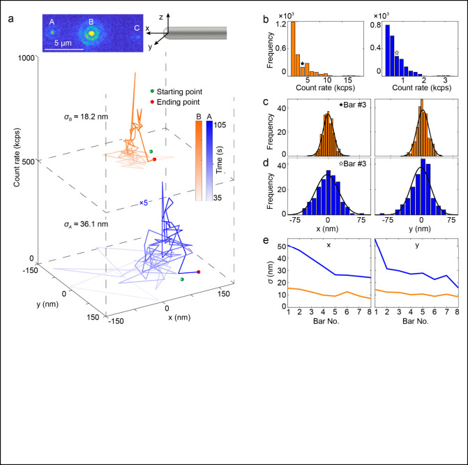
whole track A ( ) measures approximately 36.1 nm, significantly
exceeding the system’s measured accuracy. This increase is
primarily attributed to the Brownian motion experienced by the FND
prior to its stabilization within the trap. Conversely, the whole
track B shows a standard deviation (
 ) of about 18.2 nm, which is in closer alignment
with the system’s accuracy, suggesting that the scatterer at
this site remains relatively stationary and securely affixed to the
AgNW.
Figure 3.
Detailed trapping dynamics and localization analysis: (a) Trajectory mapping for the central positions of spots A (blue) and B (orange), deduced from two-dimensional Gaussian fitting applied to the PL intensity profiles. (b) Intensity-based histograms for points A and B. (c, d) Exemplary spatial distributions for particle locations at points B and A, respectively, corresponding to the PL intensity range of 4000–5000 counts per second (cps), as indicated above the third histogram bar. (e) Full width at half-maximum (fwhm) analysis for the spatial distribution of points A (blue) and B (orange) across varying intensity ranges, for x- and y-directions, respectively.
To deepen our understanding of the potential well profile derived from the trajectories, we analyzed changes in the standard deviation across various intensity ranges. Given that the emission intensity is inversely proportional to the distance from the emitter to its equilibrium position, variations in intensity provide insight into the dynamics at specific potential heights. From the standard deviations of the particle positions, we can infer the stiffness (k) of the potential well, using the equipartition theorem expressed as kBT = k⟨x2⟩, where kB is the Boltzmann constant, T is the temperature, and ⟨x2⟩ is the standard deviation of particle displacement from equilibrium.
Histograms of emission intensities from sites A and B are displayed in Figure 3b. These histograms demonstrate that within specified intensity ranges the particle positions adhere to a Gaussian distribution, as shown in Figures 3c and 3d. The corresponding standard deviations of the ith bar (σi) are detailed in Figure 3e, where the blue curves represent σ(i,A) for site A and the orange curves for σ(i,B) at site B. Specifically, when the FND particle approaches the edge of the plasmonic trap at approximately 60 s, the standard deviations of its motion at site A on the x and y axes are recorded as 50.6 and 55.5 nm, respectively. After normalization for the laser power (about 1 mW), the power-normalized stiffness values at the trap’s edge in the x- and y-directions are calculated to be 1.6 pN/nm/W and 1.4 pN/nm/W, respectively. As the particle approaches equilibrium, these deviations decrease to 24.1 nm in the x-direction and 15.8 nm in the y-direction, resulting in increased stiffness values of 7.2 pN/nm/W and 16.6 pN/nm/W. Notably, the stiffness in the y-direction exceeds that in the x-direction, highlighting the more restricted confinement of the SPP in the azimuthal and radial directions compared to the longitudinal (or axial) direction of the AgNW.
For the standard deviation at site B, depicted by the orange curves in Figure 3e, the standard deviation remains relatively consistent with the system’s measurement accuracy throughout the observation period. This consistency underscores the stability and reliability of the localization method under conditions of minimal particle motion, supporting the effectiveness of our analytical techniques in monitoring stationary scatterers within the plasmonic system.
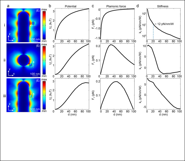
The optical trapping force can be simulated by integrating the Maxwell stress tensor across the surface of the FND nanoparticle. This calculation utilizes the field distributions derived from the finite element analysis. Among the various SPP modes supported by a nanowire waveguide, the HE1 mode is specifically chosen for this analysis, as it is predominantly excited by the tapered optical fiber coupler in aqueous conditions. Figure 4a i–iii displays the electric field distributions in both the axial and cross-sectional planes. For simplicity, the model represents the AgNW as a rounded cylinder with a circular cross-section, an approximation of its actual pentagon-shaped cross-section. The time-averaged optical forces are shown in Figure 4c, while the associated trapping potential and stiffness are derived in Figures 4b and 4d. The presence of standing waves, resulting from the interference of incident and tip-reflected SPPs, creates multiple zones of enhanced trapping along the axial direction. These zones generate a trapping force that peaks within these regions, aligning the FND nanoparticles at sites of strong plasmonic enhancement. Specifically, selecting the second interference point from the tip for illustration, it is demonstrated that the rapidly decreasing electric field in the radial direction generates a significant attractive force as the distance between the FND and AgNW decreases. This force produces a trapping potential of 3kBT with an excitation power of 1 mW, achieving a high stiffness value of up to 270 pN/(nm W) in the radial direction. The maximum stiffness values measured in the azimuthal and axial directions are 10.2 and 6.6 pN/nm/W, respectively. The measured stiffness of 16.6 pN/nm/W indicates that the trapping site is not fully aligned with the HE1 polarization.
Figure 4.
Computational assessment of trapping potentials: (a) Distribution profiles of the electric field for the HE1 mode across various cross-sectional planes. (b) Mapping of optical trapping potentials along different trajectories, as identified in panel (a). It is calculated by integrating the optical trapping forces (Fx, Fy, Fz) in (c), which are derived from Maxwell’s stress tensor. (d) Associated potential well stiffness (kx, ky, kz) exerted on the quantum dot, ascertained from the calculated force distributions.
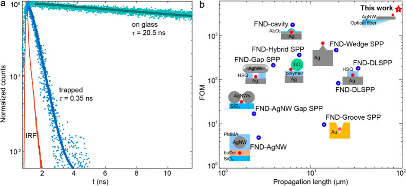
Upon the successful trapping of an FND nanoparticle on the AgNW surface, a significant enhancement in spontaneous emission was observed. The emission dynamics were precisely quantified using pulsed excitation at a wavelength of 515 nm, channeled through an optical fiber into the AgNW. The emitted PL signals were collected using an objective (NA = 0.9) to analyze the fluorescence lifetime. Details on the experiment setup are explained in the Supporting Information. As shown in Figure 5a, the emission decay profiles are accurately described by a single exponential function, which incorporates the instrument response function (IRF) to ascertain the fluorescence lifetime. This modeling approach is validated by the dominant influence of the transition into the SPP channel on the emission decay, consistent with our numerical analysis. Compared to a lifetime of 20.5 ns on a glass substrate (cyan curve), the lifetime on AgNW is drastically reduced to 0.35 ns, indicating a Purcell factor of 58.6, which aligns with the simulations in Figure 2.
Figure 5.
Photophysical characterization of the FND AgNW system. (a) Fluorescent decay curves (cyan: FNDs on glass, blue: FNDs on AgNW) with their convoluted fits and the IRF curve (red). (b) FOM and propagation length of different hybrid systems, including FND-AgNW,26 FND-AgNW Gap SPP,14 FND-Groove SPP,24,27 FND-Gap SPP,16 FND-Hybrid SPP,28 FND-Dielectric loaded SPP,11,29 FND-Wedge SPP,30 and FND-Cavity SPP.31
The enhancement factor (EF) of the plasmonic probe is estimated by comparing the steady-state emission rate from a single FND attached to AgNW to the emission rate of FNDs attached to the optical fiber (more details in the Supporting Information). We estimated the fluorescence enhancement factor through the formula23
| 4 |
It contains four determining terms
expressed as ratios of the quantum
emitter on the probe and glass. Specifically, η and η0 are the emission collection efficiencies of the imaging system,
with their ratio estimated as 1 since the same imaging conditions
are used in the measurement.  , which is ∼11.7 in this estimation,
is the electric field intensity ratio. Specifically, ESPP uses the electric field from the
launched SPP on a AgNW and E0 is calculated
from same optical power in a diffraction-limited laser spot. The ratio
between spontaneous radiation rate (
 ) is the Purcell factor from the lifetime
measurement (Figure 5).
  is the quantum yield ratio, which is ∼0.3
according to the simulations in Figure 2. Therefore, the EF can be estimated as ∼2400,
which is consistent with the observed PL enhancement during the trapping
process. More details about the experimental estimation of EF can
be found in the Supporting Information.
Further, we calculate the FOM for the coupled quantum emitter–plasmonic
waveguide system. The FOM is defined as the multiplication of the
total decay rate enhancement ( ), the energy transfer efficiency to the
plasmonic waveguide (∼35%), and the propagation length of the
SPPs normalized by the vacuum wavelength.24 The SPP mode that a dipole emitter principally excites is the HE1 mode, characterized by a substantial propagation length of
around 90 μm for the 620 nm SPP excitation on a AgNW waveguide
with a diameter of 200 nm.25 This impressive
propagation distance stems from the low scattering and ohmic losses
that are intrinsic to the atomically smooth and crystalline structure
of the waveguide. We estimate the FOM to be approximately 3000 for
this hybrid system, which stands as the highest FOM reported in current
scientific literature.11,14,16,24,26−31 This remarkable achievement is the result of an optimal blend of
substantial decay-rate enhancement and a relatively long propagation
length.
In conclusion, our work successfully demonstrated the deterministic assembly of quantum emitters onto regions of elevated plasmonic enhancement on a AgNW scanning probe via plasmonic trapping. Leveraging the superior plasmonic attributes of AgNWs, notably their significant plasmonic enhancement and minimal propagation loss, we achieved a high Purcell factor of 58.6. This leads to a spontaneous emission enhancement factor of approximately 2400 and an FOM of about 3000. This FOM is indicative of the system’s efficiency in supporting a quantum network. As an outlook, the integration of FND quantum emitters at the tip of a scanning probe paves the way for advancements in magnetic field nanoimaging and quantum information applications. These developments hold promise for not only enhancing the spatial resolution of quantum imaging but also facilitating the evolution of integrated quantum communications.
Methods
Plasmonic Trapping
A 532 nm laser beam is directed into the single-mode optical fiber used for the OF-AgNW probe. The FND solution (Adámas, carboxylated red FND, 1 wt %) is diluted 10,000-fold prior to use. The trapping process is observed and recorded using an upright optical microscope (Nikon, Eclipse Ni-U) equipped with an LU-plan Fluor 50× objective lens (NA = 0.5). For image capture, an s-CMOS camera (Andor, Zyla 5.5) is utilized. To effectively filter out the 532 nm excitation laser, we employed a long-pass filter (FEL 550, Thorlabs) in conjunction with a notch filter (NF533-17, Thorlabs). The recorded videos are captured at an exposure time of 35 ms per frame.
Acknowledgments
M.L. acknowledges support from the National Science Foundation (nos. 1654746 and 1810453). R.Y. acknowledges support from the National Science Foundation (nos. 1654794 and 2022652).
Supporting Information Available
The Supporting Information is available free of charge at https://pubs.acs.org/doi/10.1021/acs.nanolett.4c03163.
The authors declare no competing financial interest.
Supplementary Material
References
- Rittweger E.; Han K. Y.; Irvine S. E.; Eggeling C.; Hell S. W. STED microscopy reveals crystal colour centres with nanometric resolution. Nat. Photonics 2009, 3 (3), 144–147. 10.1038/nphoton.2009.2. [DOI] [Google Scholar]
- Weber M.; et al. MINSTED fluorescence localization and nanoscopy. Nat. Photonics 2021, 15 (5), 361–366. 10.1038/s41566-021-00774-2. [DOI] [PMC free article] [PubMed] [Google Scholar]
- Liu X.; Braun G. B.; Qin M.; Ruoslahti E.; Sugahara K. N. In vivo cation exchange in quantum dots for tumor-specific imaging. Nat. Commun. 2017, 8 (1), 343. 10.1038/s41467-017-00153-y. [DOI] [PMC free article] [PubMed] [Google Scholar]
- Zhao J.-Y.; et al. Ultrasmall Magnetically Engineered Ag2Se Quantum Dots for Instant Efficient Labeling and Whole-Body High-Resolution Multimodal Real-Time Tracking of Cell-Derived Microvesicles. J. Am. Chem. Soc. 2016, 138 (6), 1893–1903. 10.1021/jacs.5b10340. [DOI] [PubMed] [Google Scholar]
- Wells N. P.; et al. Time-Resolved Three-Dimensional Molecular Tracking in Live Cells. Nano Lett. 2010, 10 (11), 4732–4737. 10.1021/nl103247v. [DOI] [PMC free article] [PubMed] [Google Scholar]
- Zhang L.-J.; Xia L.; Xie H.-Y.; Zhang Z.-L.; Pang D.-W. Quantum Dot Based Biotracking and Biodetection. Anal. Chem. 2019, 91 (1), 532–547. 10.1021/acs.analchem.8b04721. [DOI] [PubMed] [Google Scholar]
- Yang C. H.; et al. Operation of a silicon quantum processor unit cell above one kelvin. Nature 2020, 580 (7803), 350–354. 10.1038/s41586-020-2171-6. [DOI] [PubMed] [Google Scholar]
- Uppu R.; Midolo L.; Zhou X.; Carolan J.; Lodahl P. Quantum-dot-based deterministic photon-emitter interfaces for scalable photonic quantum technology. Nat. Nanotechnol. 2021, 16 (12), 1308–1317. 10.1038/s41565-021-00965-6. [DOI] [PubMed] [Google Scholar]
- de Torres J.; Ferrand P.; Colas des Francs G.; Wenger J. Coupling Emitters and Silver Nanowires to Achieve Long-Range Plasmon-Mediated Fluorescence Energy Transfer. ACS Nano 2016, 10 (4), 3968–3976. 10.1021/acsnano.6b00287. [DOI] [PubMed] [Google Scholar]
- Tran T. T.; et al. Facile Self-Assembly of Quantum Plasmonic Circuit Components. Adv. Mater. 2015, 27 (27), 4048–4053. 10.1002/adma.201501142. [DOI] [PubMed] [Google Scholar]
- Siampour H.; et al. On-chip excitation of single germanium vacancies in nanodiamonds embedded in plasmonic waveguides. Light: Science & Applications 2018, 7 (1), 61. 10.1038/s41377-018-0062-5. [DOI] [PMC free article] [PubMed] [Google Scholar]
- Huck A.; Kumar S.; Shakoor A.; Andersen U. L. Controlled Coupling of a Single Nitrogen-Vacancy Center to a Silver Nanowire. Phys. Rev. Lett. 2011, 106 (9), 096801. 10.1103/PhysRevLett.106.096801. [DOI] [PubMed] [Google Scholar]
- Ratchford D.; Shafiei F.; Kim S.; Gray S. K.; Li X. Manipulating Coupling between a Single Semiconductor Quantum Dot and Single Gold Nanoparticle. Nano Lett. 2011, 11 (3), 1049–1054. 10.1021/nl103906f. [DOI] [PubMed] [Google Scholar]
- Kumar S.; Huck A.; Andersen U. L. Efficient Coupling of a Single Diamond Color Center to Propagating Plasmonic Gap Modes. Nano Lett. 2013, 13 (3), 1221–1225. 10.1021/nl304682r. [DOI] [PubMed] [Google Scholar]
- Kumar S.; Kristiansen N. I.; Huck A.; Andersen U. L. Generation and Controlled Routing of Single Plasmons on a Chip. Nano Lett. 2014, 14 (2), 663–669. 10.1021/nl403907w. [DOI] [PubMed] [Google Scholar]
- Kumar S.; Andersen S. K. H.; Bozhevolnyi S. I. Extremely Confined Gap-Plasmon Waveguide Modes Excited by Nitrogen-Vacancy Centers in Diamonds. ACS Photonics 2019, 6 (1), 23–29. 10.1021/acsphotonics.8b01225. [DOI] [Google Scholar]
- Geiselmann M.; Marty R.; Renger J.; García de Abajo F. J.; Quidant R. Deterministic Optical-Near-Field-Assisted Positioning of Nitrogen-Vacancy Centers. Nano Lett. 2014, 14 (3), 1520–1525. 10.1021/nl4047587. [DOI] [PubMed] [Google Scholar]
- Chang D. E.; Sørensen A. S.; Hemmer P. R.; Lukin M. D. Quantum Optics with Surface Plasmons. Phys. Rev. Lett. 2006, 97 (5), 053002. 10.1103/PhysRevLett.97.053002. [DOI] [PubMed] [Google Scholar]
- Issa N. A.; Guckenberger R. Fluorescence near metal tips: The roles of energy transfer and surface plasmon polaritons. Opt. Express 2007, 15 (19), 12131–12144. 10.1364/OE.15.012131. [DOI] [PubMed] [Google Scholar]
- Kim S.; Yan R. Recent developments in photonic, plasmonic and hybrid nanowire waveguides. Journal of Materials Chemistry C 2018, 6 (44), 11795–11816. 10.1039/C8TC02981D. [DOI] [Google Scholar]
- Ma X.; et al. 6 nm super-resolution optical transmission and scattering spectroscopic imaging of carbon nanotubes using a nanometer-scale white light source. Nat. Commun. 2021, 12 (1), 6868. 10.1038/s41467-021-27216-5. [DOI] [PMC free article] [PubMed] [Google Scholar]
- Chang D. E.; Sørensen A. S.; Demler E. A.; Lukin M. D. A single-photon transistor using nanoscale surface plasmons. Nat. Phys. 2007, 3 (11), 807–812. 10.1038/nphys708. [DOI] [Google Scholar]
- Hoang T. B.; et al. Ultrafast spontaneous emission source using plasmonic nanoantennas. Nat. Commun. 2015, 6 (1), 7788. 10.1038/ncomms8788. [DOI] [PMC free article] [PubMed] [Google Scholar]
- Bermúdez-Ureña E.; et al. Coupling of individual quantum emitters to channel plasmons. Nat. Commun. 2015, 6 (1), 7883. 10.1038/ncomms8883. [DOI] [PMC free article] [PubMed] [Google Scholar]
- Kim S.; Bailey S.; Liu M.; Yan R. Decoupling co-existing surface plasmon polariton (SPP) modes in a nanowire plasmonic waveguide for quantitative mode analysis. Nano Research 2017, 10 (7), 2395–2404. 10.1007/s12274-017-1438-1. [DOI] [Google Scholar]
- Akimov A. V.; et al. Generation of single optical plasmons in metallic nanowires coupled to quantum dots. Nature 2007, 450 (7168), 402–406. 10.1038/nature06230. [DOI] [PubMed] [Google Scholar]
- Kumar S.; et al. Efficient Coupling of Single Organic Molecules to Channel Plasmon Polaritons Supported by V-Grooves in Monocrystalline Gold. ACS Photonics 2020, 7 (8), 2211–2218. 10.1021/acsphotonics.0c00738. [DOI] [Google Scholar]
- Kumar S.; Bozhevolnyi S. I. Excitation of Hybrid Plasmonic Waveguide Modes by Colloidal Quantum Dots. ACS Photonics 2019, 6 (7), 1587–1593. 10.1021/acsphotonics.9b00379. [DOI] [Google Scholar]
- Siampour H.; Kumar S.; Bozhevolnyi S. I. Nanofabrication of Plasmonic Circuits Containing Single Photon Sources. ACS Photonics 2017, 4 (8), 1879–1884. 10.1021/acsphotonics.7b00374. [DOI] [Google Scholar]
- Kress S. J. P.; et al. Wedge Waveguides and Resonators for Quantum Plasmonics. Nano Lett. 2015, 15 (9), 6267–6275. 10.1021/acs.nanolett.5b03051. [DOI] [PMC free article] [PubMed] [Google Scholar]
- Chiang C.-C.; et al. Chip-Compatible Quantum Plasmonic Launcher. Advanced Optical Materials 2020, 8 (20), 2000889. 10.1002/adom.202000889. [DOI] [Google Scholar]
Associated Data
This section collects any data citations, data availability statements, or supplementary materials included in this article.


