Abstract
Ultra-wideband (UWB) technology is extensively used in indoor navigation, medical applications, and Internet of Things devices due to its low power consumption and resilience against multipath fading and losses. This paper examines a multiple-input multiple-output (MIMO), circularly polarized (CP) dielectric resonator antenna for UWB systems. Compact form factor, high gain, wideband response, improved port isolation, and high data rates are the major design goals. This arrangement consists of two identical DRAs with self-decoupled orthogonal orientations eliminating the need for extra decoupling structures while achieving an impressive maximum isolation of 43 dB. The corner-edge feeding mechanism of the extended feedline generates two orthogonal E-fields, facilitating circular polarization. Additionally, a printed hook-shaped stub integrated with the ground plane enhances CP performance across the two operating bands without altering the DR structure. Fabrication and testing exhibit an impressive 133 impedance bandwidth (2.5–14 GHz) with high port isolation. For a 3 dB axial ratio reference, the single-element design exhibits axial ratio bandwidths (ARBW) of 1.2 GHz (3.6–4.8 GHz) and 0.8 GHz (9.3–10.1 GHz). Remarkably, the MIMO configuration achieves a single ARBW of 0.5 GHz (3.9–4.4 GHz). Detailed investigations of MIMO performance parameters, including diversity gain, envelope correlation coefficient, channel capacity loss, and total active reflection coefficient, underscore the design’s efficacy, making it a good choice for UWB wireless applications.
Keywords: MIMO Antenna, DRA
Subject terms: Engineering, Applied physics
Introduction
Considering the exponential growth in the number of wireless devices and their limited bandwidth, the development of antenna technology for establishing effective wireless communication is more significant than ever. The simplest choice to equip wireless devices is with single input and single output (SISO) antennas, which have many shortcomings, such as low gain, low efficiency, and low data rates. In contrast to that, wireless devices equipped with compact MIMO antennas offer pattern diversity, polarization diversity, and high data rates. However, compact MIMO antennas potentially suffer from low mutual coupling, which affects their overall performance. To address this issue, numerous research works highlighting the antenna compactness and performance have been reported in the literature. The typical architectural approaches include defective ground structures (DGS)1–5 metallic vias in the dielectric resonators (DR)6,7, inserting metamaterials between the DRs8,9, or adding metallic structures of different orientations to the DR10,11. Substrate integrated waveguide (SIW) and CSSR techniques are equally helpful in achieving compactness, multiband operation, gain enhancement and introducing circular polarization.12–14
A circularly polarized DR antenna for mm-wave 5G application has been proposed in15. The reported design operates from 28.26 to 30.26 GHz with a percentage bandwidth of 26.3 % below -10 dB. The DRA has been placed on top of Roger as a substrate material with total dimensions of 5.76 × 6.76 × 0.254 mm3. The proposed design has the drawback of a complex design with a bulky shape. Furthermore, a triple-band MIMO DR antenna using an aperture couple feeding mechanism has been reported in16. The reported design has a 100 ×100 ×1.6 mm3 geometry using FR4 substrate as a dielectric material. The suggested design operates from 1.63 to 1.84 GHZ, 2.43 to 2.71 GHZ, and 3.28 to 3.73 GHZ with a bandwidth of 0.2GHz, 0.28GHz and 0.45 GHz, respectively. The proposed design has the drawback of being very large, having no UWB features, complex shape, no CP performance, and without studying link budget analysis. Thus complex structure and bulky size make it difficult to house the design in wireless devices. In17, a circularly polarized MIMO DRA using an offset feeding is presented. The proposed design has dimensions of 40 ×60 ×1.6 mm3 using FR4 as a substrate. The proposed design operates from 5.12 to 6.12 GHz with a total bandwidth of 0.9 GHz and axial ratio of 5.31–6.60 GHz with a gain of 4.4 dBi. Because of numerous stresses, a rectangular slot in the DR makes the fabrication difficult. Overall the design has a bulky shape with no link budget estimation. The design covers a narrow band and requires numerous changes to achieve the UWB band with MIMO characterization. A stacked cylindrical DR using a conformal-shaped microstrip feedline with the truncated ground plane is reported in18. The proposed design has used FR4 as a dielectric material with an overall geometry of 40×40 ×1.6 mm3. The operational bandwidth of the proposed design is 3.65–7.8 GHz (72.48%) with an AR of 4.38–6.86 GHz (44.12%). The suggested design has the drawback is its SISO arrangement, large geometry with complex shape with no UWB features, and link budget analysis. UWB antennas are particularly significant in applications where traditional narrowband or broadband antennas face limitations, such as in ultra-high-speed wireless networks, radar systems, medical imaging, and IoT devices. Due to high gain, wide impedance bandwidth, and 3D structure, DRAs are preferred over conventional microstrip patch antennas. Therefore, it is important to study UWB DRAs in detail. Numerous single and multiport wideband and UWB DRAs have been reported in the literature10,15,19–26. In27 a compact DRA is used as a filter antenna, showing its potential to work as a filter and antenna for different wireless applications. In19 copper rings are used with DRA to excite multimode within the DRA. This helps to achieve multiband operation from a single design. In20, a single-feed CP DRA for multiband wireless applications has been proposed. The design is a hybrid structure where copper patches have been added to achieve circular polarization. Despite good performance and CP operation, the bulky size (0.25 0.29 0.22) of the DR makes it difficult to house the design in wireless devices. A wideband CP DRA for 5G mm-wave applications has been proposed in15. The edge feeding mechanism and trapezoidal cutting of the DR enable CP radiation. Nonetheless, a costly and complex fabrication procedure, along with low gain and CP performance, reduces the usefulness of the design for 5G applications. In21, the orthogonal modes are generated by adding two annular vias within the DR. This technique enhances both the CP performance and gain of the design. Recent research findings show that MIMO antennas offer higher spectrum efficiency as compared to SISO devices. Without increasing the input power or bandwidth, MIMO antennas provide increased channel capacity over SISO antennas. In the literature, several MIMO architectures have been studied. A two-port MIMO CP DRA is proposed in10. The annular vias and z-shaped strip have generated two orthogonal modes, making the design circularly polarized. A self-decoupled linearly polarized MIMO DRA at 5.8 GHz is presented in22. A two-port MIMO DRA with a stub between the DRs for port isolation is proposed in23. The orthogonally positioned DRA isolation is further enhanced by suppressing the current flow between ports using a stub. In a study conducted in24, two ultra-wideband (UWB) antenna elements are positioned in a perpendicular arrangement to achieve polarization diversity, which also ensures a high level of isolation between them. To further improve the port’s isolation, a T-shaped strip is employed as a decoupling structure for this MIMO setup. In25, a metallic strip is inserted between the two identical staircase-shaped printed radiating elements, which helps to attain a high level of isolation. The suggested design has a small footprint of 25 30 mm while attaining the UWB band. A large-heightened dual mode CP DRA of the dimensions 40x40x18 mm2 with stair-shaped microstrip fed line is presented in26. The aforementioned DRAs offer good performance at the expense of either increased size or design complexity. It is important to note that achieving high port isolation without a decoupling technique is challenging. As of now, the literature does not offer any UWB antenna solution with MIMO, CP, and high port isolation achieved simultaneously. To enhance the effectiveness of the UWB technology, it is important to develop MIMO antennas featuring high data rates, low mutual coupling, and circular polarization. In particular, simple and cost-effective UWB MIMO DRAs with high port isolation and good CP performance are in high demand. As mentioned, the literature has reported very limited selection of UWB MIMO CP DRAs, making limited options for the detailed analysis. In this work, we propose a two-port UWB MIMO DRA characterized by compact size, enhanced port isolation, and wide axial ratio bandwidth, designed to meet the diverse requirements of UWB technology in various real-time applications. Our proposed design exhibits several distinctive attributes. To achieve these goals, we introduce a novel feedline extended along the edges of the DR, generating orthogonal electric fields. This unique field orientation initially induces CP operation within the DRA, which is further enhanced by adding a hook-shaped strip on the ground side. The design is then extended to MIMO configuration through orthogonal arrangement and 90-degree rotation of antenna elements which enhance the data rate and port isolation without adding any decoupling structure. As shown in Fig. 1, the design evolves from a simple microstrip-fed DRA, extended around the DR, featuring a novel compact CP architecture. Interestingly, the design has a very wide operating band from 2.5 to 14 GHz. With a maximum efficiency of around 92%, the proposed design offers a gain of over 3.5 dBi throughout the entire operating band while preserving a consistent radiation pattern. A measured diversity gain surpassing 9.98 and an envelope correlation coefficient (ECC) below 0.003 indicates the potential of our design in forthcoming medical and IoT applications. Recently published designs have shortcomings in terms of design compactness, performance and cost. Miniaturization has been achieved either by cutting DR into different shapes or by adding additional structure such as EBG to the DR. This is an expensive solution which although shift the resonance frequency to low range but increase the physical size. Similarly, we have MIMO DRAs to enhance the data rate but at the same time, complex techniques have been adopted to reduce the mutual coupling. Lack of CP feature makes these MIMO design useless for many important wireless applications. The novelty of the proposed design is the intelligent use of simple and cost effective techniques to achieve very wide band which not only cover UWB but also X-band and a part of S-band. Moreover, CP performance with MIMO characterization are two additional features which makes the proposed design superior to the existing published models.
Fig. 1.
The proposed 2-port UWB MIMO antenna system.
The primary contributions of this study may be summed up as follows:
The SISO arrangement of the proposed design is analyzed in detail, offering a very wide band, high gain, compact size, and two CP bands with good axial ratio performance.
The proposed design is converted to MIMO DRA array configuration, significantly enhancing the data rate and channel capacity.
To the best of the author’s knowledge, the design has competitively compact DRs (for UWB application) in terms of electrical length compared to published works
The proposed design offers a wide operating band (2.5–14 GHz) compared to the conventional 3.1–10.6 GHz UW band.
The proposed design is the first UWB DRA that has simultaneously achieved compactness, MIMO performance, and CP features while maintaining high port isolation without adding any decoupling technique. This makes the design simpler and cost-effective.
The compact size, high radiation efficiency, and CP features of the proposed design has the potential to address the path loss issue.
To the author’s knowledge, the detailed link budget analysis is performed for the first time for the proposed design, confirming its suitability for UWB wireless applications.
The remaining parts of the work are organized as follows. Section Proposed design overview and design steps presents the proposed MIMO DRA overview and design steps. Section Parametric analysis gives a detailed analysis of the design parameters. Section Antenna performance evaluation using full-wave simulation and measurements highlights the simulation and measurement results. Section MIMO parameters explains the MIMO parameter. Section Link budget analysis overviews the link budget analysis, whereas Section Conclusion concludes the work.
Proposed design overview and design steps
Antenna configuration
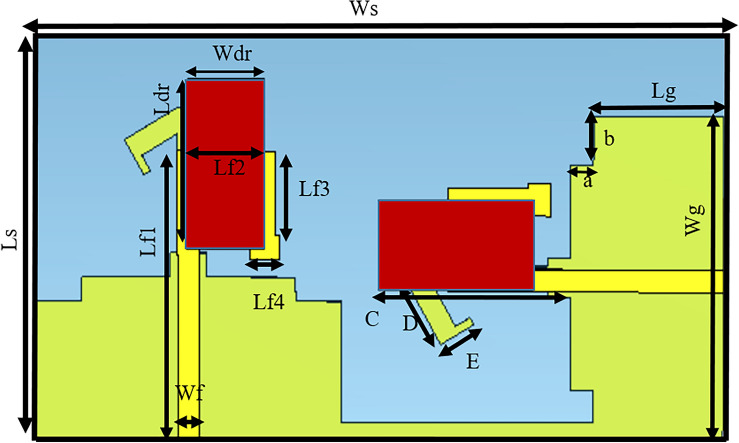
The detailed geometry of the proposed UWB MIMO DRA with extended feedline around the edges of the DR is given in Fig. 1. The proposed design comprises two port DRA positioned orthogonally to each other. Each DR has a microstrip feed line excitation extended around the DR edges for orthogonal modes excitation. The reduced ground plane generates a wide impedance bandwidth with a hook-shaped stub, which improves the axial ratio performance. A thin strip line between each MIMO ground provides a common reference point for the voltage. The DRs utilized in this study consist of Rogers substrates with a relative permittivity of 10. The feedline and hook-shaped stub are printed on an FR4 substrate with a permitivity of 4.4, tangent loss of 0.002, and 1.6 mm standard thickness. The overall dimensions of the proposed UWB MIMO CP DRA substrate are 50 90 1.6 mm3 (), where is the length of the substrate, is the width of the substrate, and is the height of the substrate. The dimensions of DR are 20 105 mm3 (). To provide common ground, the ground plane of each DRA is connected to other with 1 mm-thick microstrip line. The dimensions of the detailed geometry are listed in Table 1.
Table 1.
Optimized design parameters of proposed design.
| Parameters | Dimensions (mm) | Parameters | Dimensions (mm) |
|---|---|---|---|
| 50 | 20 | ||
| 90 | 40 | ||
| 1.6 | A | 3 | |
| 20 | B | 60 | |
| 10 | C | 21 | |
| 36 | D | 8 | |
| 10 | 2.2 | ||
| 7.7 | 1 | ||
| 4 | 2.8 |
Design equations
The single element of the proposed UWB MIMO DRA is predicated on the synergistic integration of two key components: the DR, serving as the primary radiator, and the feedline, responsible for exciting the DR to emit radiation. The design of both entities is underpinned by specific mathematical formulations. The DR, initially modeled as a waveguide, is governed by equations derived from the Dielectric Waveguide Model (DWM). The DRAs and waveguides work on the same principle. Both share many common properties as both are rectangular and have three dimensions with two degrees of freedom. There is no separate theory for DRA, and the initial dimensions of the DRA are based on the dielectric waveguide model (DWM). A DRA is like a waveguide filled with dielectric materials. Any feeding option disturbs the quality factor of the DR, enabling different operating modes within the DR. The three dimensions (Length, Width, and Height) of the rectangular DR in the proposed design are based on the following equations28.
| 1 |
Where
| 2 |
In (2) ,, are wave numbers in three cartesian directions given by Eqs. (3–5), is relative permittivity of the DR material, is free-space wave number, while and are the vacuum permeability and permittivity, respectively.
| 3 |
| 4 |
| 5 |
It is important to note that m, n, and p are the integers while a, b, and d are the three dimensions (Length, Width, and height) of the proposed DR. The calculation of the initial dimensions depends on many factors, including DR availability and overall cost. Once the DR with specific dimensions is finalized, the next step is to excite it using any excitation technique (coaxial probe, slot aperture, or microstrip feedline). In this work, the DR is excited with a 50 microstrip line. The 3.14 mm width of the extended feedline is obtained as follows:
| 6 |
In (6), is the characteristic impedance of the feedline, is the width of the feedline, is the relative permittivity of the substrate and is the height of the substrate.
Design evolution and working principles
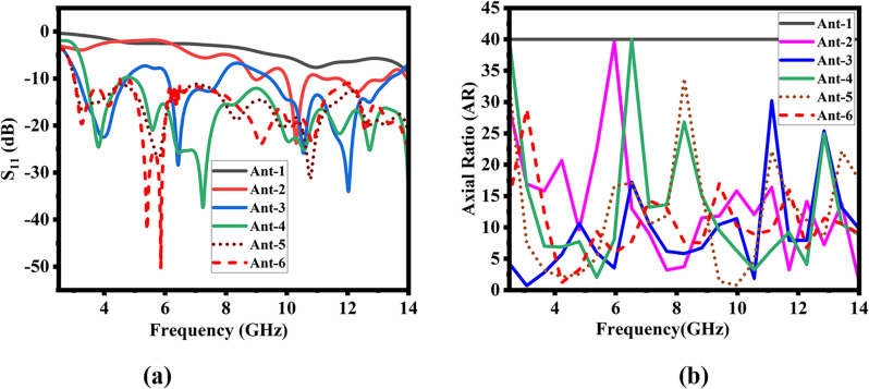
The overall design evolution of the proposed UWB MIMO CP DRA progresses through six steps, detailed in this section. Figure 2 presents full design evolution steps and their impact on the simulated results with Ant.1, Ant.2, Ant.3, Ant.4, Ant.5, and Ant.6 respectively. Their corresponding simulated results regarding reflection coefficients and axial ratio (AR) are shown in Fig. 3a,b, respectively. Ant-1, which is the basic framework, consists of a truncated ground and a rectangular DRA excited by a microstrip feed line with a 50-ohm characteristic impedance. Figure 3a shows the corresponding simulated results of Ant-1. At this stage, the design tends to resonate at a single resonance frequency beyond 14 GHz with no CP performance. In the second step (Ant-2), the feedline position is changed from the center to the edge of the DRA. In addition, on the ground side, a vertical stub is added to the middle of the partial ground. This configuration produces orthogonal modes inside the DR, circularly polarizing the design. At this stage, the design has a single operating band at 10.3 GHz with low impedance matching. Although the design at this stage has exhibited the CP nature, there is still a need to improve the axial ratio and impedance bandwidth. In step 3 (Ant-3) of the proposed design, the microstrip feed line is further extended to the other edges of the DR. Moreover, adding a metallic strip with bent to the ground stub improves the impedance bandwidth, resonating at 3.6 GHz, 6.09 GHz, 9.2 GHz, and 13.4 GHz, respectively. This stage makes the design dual band CP at 2.2–3.2 GHz and 10.3–10.4 GHz respectively. Analyzing the electric field distribution inside the DR, in Step 4 the DR is moved slightly upward such that the extended feedline now passes through the center of the DRA. This step makes the design UWB have CP performance at two bands. Step 5 further enhances CP performance by increasing the axial ratio bandwidth. Step 6 involves transforming the design into a MIMO configuration, effectively addressing data rate concerns. In the case of the MIMO antenna, it is important that all radiators have a common reference point. In case of not connected ground plane, the MIMO elements will be considered independent which is technically erroneous. To avoid this a thin microstrip line connects all the partial ground planes, giving them a common reference point. However, it is important to note that this orthogonal arrangement of the antenna elements for MIMO configuration has suppressed the orthogonal electric fields at higher frequencies. Consequently, the second CP band axial ratio performance has been degraded.
Fig. 2.
Different design steps of the proposed UWB CP DRA. (Ant-1 the basic design with center excitation, Ant-2 edge excitation of the DR with extended feedline, Ant-3 DR with extended feedline and addition of stub with the ground, Ant-4 is moving DR upward on the feedline, Ant-5 shows bent shaped strip with ground stub and Ant-6 is the MIMO arrangement of the proposed design).
Fig. 3.
(a) Scattering parameters of different stages (b) 3dB Axial Ratio of different design steps.
Equivalent circuit model
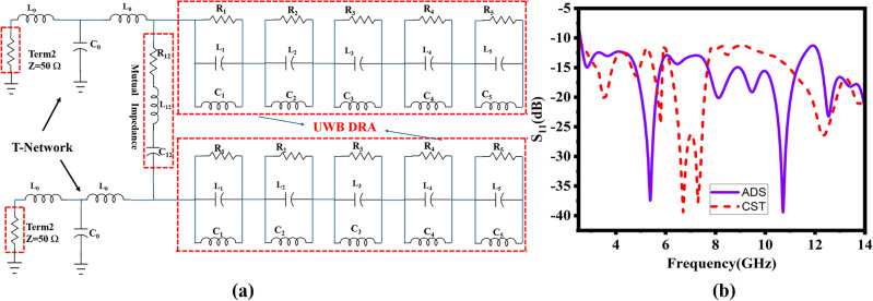
Determining the lumped model elements of the rectangular DRA depends on many important factors, which include operating modes, material of the DR and type of excitation (feeding). The rectangular DRA can be modeled with an equivalent circuit, which comprises of inductors (L), capacitors (C) and resistors (R). For simple DRA (similar to microstrip patch antenna) resonating on a single frequency, LC tank circuit is a proper manifestation to explain its working principal. In case of broadband or wide band DRAs, we need multiple cascaded LC circuits to reflect the similar concepts. Advance Design System (ADS) is helpful to produce and validate the equivalent circuit of the proposed DRA S11. As our MIMO design elements replicate each other, therefore only one element equivalent circuit is described and its S11 simulated result is reproduced in ADS as depicted in Fig. 4a,b. Equation (7–8)29 are used to determine the transmission line capacitance (C0) and inductance (L0). The resonance frequency for DRA can be calculated from DWM model. Equation (9–10)29 are used to determine the inductance and capacitance for the lumped model circuit of DRA. The real and imaginary impedance values, helpful in lumped circuit element calculation are imported from CST. After combining and tuning lumped circuit elements in ADS, it is realized that both simulated results from CST and ADS have close agreement as shown in Fig. 4b. While the values calculated for the lumped model, circuit can be summed up as: Lo=0.202 nH, Co=0.13 pF, R1=40.12 , L1=1.12 nH, C1=6.70066 pF, R2=30.8 , L2=12.31 nH, C2=6.70066 pF, R3=31.55 , L3=13.11 nH, C3=2.46236 pF, R4=43.16 , L4=14.11 nH, C4=2.67002 pF, R5=61.12 , L5=15.23 nH, C5=0.9313 pF.
| 7 |
| 8 |
| 9 |
| 10 |
Fig. 4.
(a) Equivelnt circuit (b) Simulated S11 results comparison of CST and ADS.
Parametric analysis
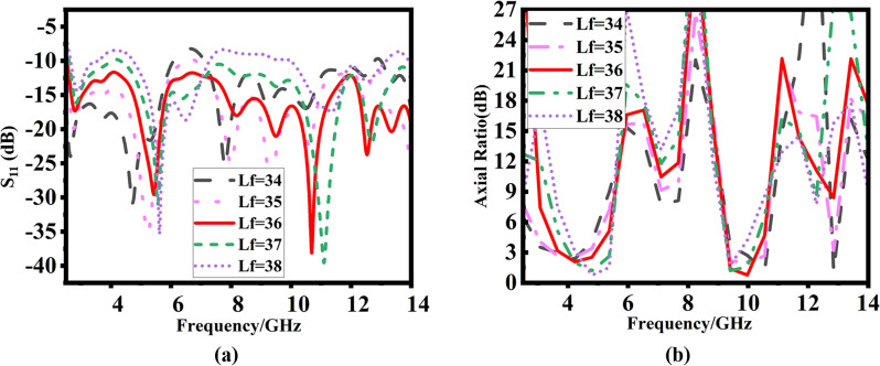
A comprehensive parametric study is conducted to assess the impact of various parameters on the performance of the antenna, which includes variations in feed line configuration, alterations in the position of the DR along the feed line, changes in the angle of the stub bend, and adjustments to the height of the DR. Analysis of these parameters focuses on their effects on the reflection coefficient and axial ratio of the antenna. The impact of feedline variation on the reflection coefficient and axial ratio is shown in Fig. 5a,b. A gradual increase in the feedline length significantly enhances the impedance matching and axial ratio. The smaller feedline length results in low impedance matching and axial ratio. At Lf of 36 mm length, the proposed design has better impedance matching and axial ratio performance. Further increase in the feedline length disturbs the impedance matching but generates a third axial ratio bandwidth. However, to maintain the UWB behavior of the proposed design, a 36 mm length is chosen to be final value of the feedline.
Fig. 5.
Effect of length of mounted feed: (a) return loss, (b) axial ratio.
Impact of variation in the DR position
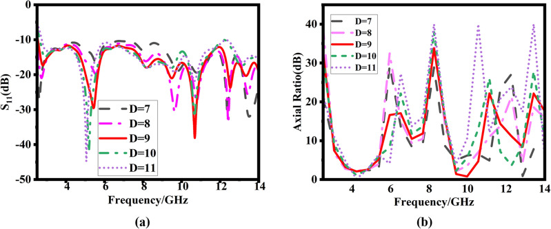
Changing the DR position on the feedline also impacts the impedance matching and axial ratio bandwidth. Figure 6a,b highlight changing the DR position on the feedline. Gradually moving DR upward on the feedline improves the impedance matching and enhances the AR performance. The maximum impedance matching and axial ratio bandwidths are achieved at the position where the feedline crosses the DR center. Further moving the DR upward reduces the impedance matching and narrows the axial ratio bandwidth.
Fig. 6.
Effect of DRA position on (a) return loss, (b) axial ratio.
Impact of variation in the bent angle of the L-shaped strip
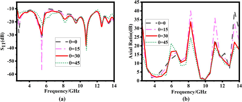
Another important parameter is the bent angle of the L-shaped strip in the truncated ground plane. It is important to note that this parameter greatly affects the axial ratio performance while affecting the reflection coefficient, as shown in Fig. 7. The AR performance is better at q = but it has a narrow bandwidth at lower frequencies. Gradual increase in the bent angle increases the impedance matching and axial ratio performance. The maximum response is observed at a bent angle of . Any further increase in the angle degrades both the performance parameters. Therefore, an angle of is finalized for the suggested design.
Fig. 7.
Effect of the L-shaped bend angle on (a) return loss and (b) axial ratio.
Impact of DR Height
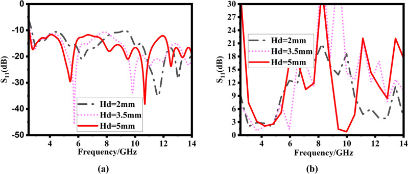
The effect of DR height on the return loss and axial ratio performance is studied in this section. Figure 8 shows that a gradual increase in the DR height enhances the impedance matching and axial ratio bandwidth range. At 5 mm DR height, the UWB with better impedance matching and two axial ratio bandwidth is achieved. With the available resources, a maximum of 5 mm DR height is selected for the final design.
Fig. 8.
Effect of variation of height of DR on (a) return loss, (b) axial ratio.
Antenna performance evaluation using full-wave simulation and measurements
This section comprehensively assesses the performance of the proposed design using simulation and measurement data. Across the UWB spectrum, various performance metrics such as reflection coefficients, radiation patterns, current distributions, gain, and efficiency are analyzed. Additionally, the port isolation coefficient between antenna elements is examined to evaluate their interconnection.
Experimental setup
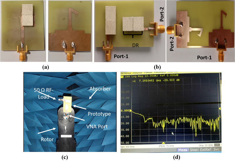
An electromagnetic tool, CST Microwave Studio, is used to model, simulate, and analyze the proposed MIMO array architecture. The proposed design is fabricated and measurements are conducted to validate the simulated outcomes. An anechoic chamber is used to measure the antenna gain performance. When performing the measurements, a vector network analyzer (VNA) is utilized, which enables precise reflection coefficient characterization and other important features, as illustrated in Fig. 9. One port of the proposed antenna prototype is terminated with a 50 matching load.
Fig. 9.
Fabricated antenna prototype and experimental validation: (a) single element (top and bottom views), (b) MIMO design (top and bottom views), (c) antenna in the anechoic chamber, (d) VNA-measured reflection characteristic.
Scattering parameters
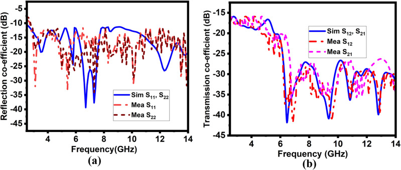
This section overviews the simulated and measured scattering parameters of the proposed design. These include the reflection coefficients and mutual coupling between the ports. The scattering parameters were measured by connecting the prototype to a Vector Network Analyzer (VNA). Figure 10a,b show the simulated and measured scattering parameters. Figure 10a shows that the simulated reflection coefficient (S11) has a 12.5 GHz impedance bandwidth for a dB reference value. The measured S11 also covers the same operating band with better impedance matching. The simulated and measured mutual impedance has also maintained a close agreement, however, a minor deviation is there at the lower band. This is due to inaccurate fabrication and the impact of surrounding noise during measurement. A minimum of 15 dB and a maximum of 43 dB isolation is attained over the UWB. Despite minor deviation, there is a strong correlation between the experimental and simulation results, indicating the reliability of EM analysis. Table 2 summarizes the scattering parameters with all relevant information.
Fig. 10.
(a) shows simulated and measured reflection coefficients (b) shows simulated and measured mutual coupling.
Table 2.
Simulated and measured S-parameters.
| Results | Resonating Freq. (GHz) | Bandwidth (GHz) | (dB) | (dB) |
|---|---|---|---|---|
| Simulated | 3.7, 5.8, 6.8, 10.3, 12.2 | 2.45 − 14 | < 17 | < 17 |
| Measured | 3, 5.2, 7.2, 10, 13.5 | 2.6 − 14 | < 16 | < 17 |
Gain and axial ratio
When examining antenna performance, the antenna’s gain is a crucial factor to consider, which provides useful information concerning the efficiency of power transmission between the transmitter and the receiver. The proposed design’s simulated and measured gain across the operating band is detailed in Fig. 11a. The measured and simulated findings are in good agreement. Across the operating band, an average gain of more than 3.5 dBi is attained, and around 7.2 GHz, a maximum measured gain of 5.5 dBi is observed. Initially, there is a gradual increase in the gain due to the dominant effect of the DR, attaining a maximum value of 7.2 GHz. A decline in gain beyond this frequency is noticed, showing the microstrip’s dominant effect. Thus, the overall gain reflects the hybrid nature of the proposed design. On the other hand, there are minor discrepancies between simulated and measured gain around 9 GHz and 13 GHz range, which can be attributed to factors such as human error, cable losses, and manufacturing imperfections. Despite the slight variation between observed and simulated gain, the effectiveness of the proposed design remains substantiated. Similarly, the simulated and measured axial ratio of the single element and MIMO are detailed in Fig. 11b,c. A single element of the proposed design has two wide axial ratio bandwidths, while the MIMO design has a single axial ratio bandwidth with a relatively narrow response. It is important to note that the circular polarization behavior is due to the existence of the orthogonal electric fields. In the case of the MIMO arrangement of the antenna, the orthogonal electric field modes of the one port are suppressed by the second port. The amount of suppression either vanishes the CP band or reduces the CP performance. In our case, the MIMO arrangement has highly degraded the upper band CP performance while slightly narrowing down the lower band CP performance. Thus, the cancellation effect is dominant in higher frequencies. The details of the measured and simulated gains are summarized in Table 3.
Fig. 11.
Simulated and measured results of the proposed design (a) Gain of single antenna element (b) Axial Ratio of Single antenna element (c) Axial Ratio of proposed MIMO design.
Table 3.
Simulated and measured gain and axial ratio of the proposed design.
| Results | Peak Gain (dB) | AR BW (SISO) | AR BW (MIMO) |
|---|---|---|---|
| Simulated | 5.04 | 3.6 − 4.8, 9.3 − 10.1 | 3.9 − 4.4 |
| Measured | 5.5 | 3.9 − 4.9, 9.24 − 10.3 | 3.86 − 4.54 |
Electric field distribution
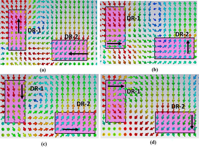
The electric field distribution within the DR gives a detailed overview of the CP behavior of the proposed design. The E-field distributions during a quarter of the period at 4.2 GHz are shown in Fig. 12. Due to low DR height, analyses of the E-field distribution are only carried out on the DR top surface. One port of the DR is excited, while the second is terminated with a 50 matching load. As shown in Fig. 12a,b,c,d, the E-field distribution is observed at , , and respectively. The analysis shows that each DR has maintained orthogonal E-field distribution at both , as shown in Fig. 12a,b and , as given in Fig. 12c,d respectively. Additionally, DR 2 exhibits minimal electric field activity for both observations, indicating low coupling and effective isolation between the MIMO elements.
Fig. 12.
E-field distribution of the proposed design at 4.2 GHz. (a) and (b) shows the current distribution at and phases while (c) and (d) shows the current distribution at and respectively.
Far field radiation pattern
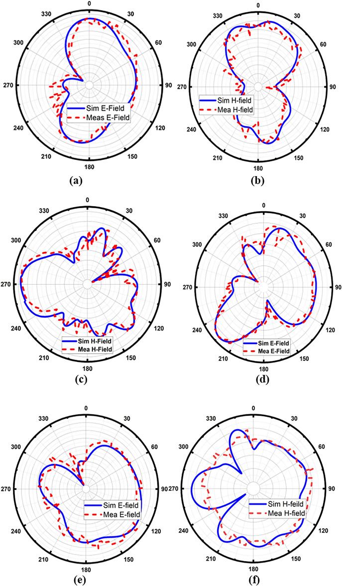
Figure 13 shows the 2D radiation pattern of the proposed design at 4.2 GHz, 6.5 GHz, and 12 GHz, respectively. While measuring the far field patterns, port 1 is excited while port two is terminated with 50 load. Figure 13a,b illustrate the E-field and H-field at 4.2 GHz, respectively, depicting the circular polarization of the proposed MIMO design. At this frequency, the E-field exhibits a broad and focused orientation towards 0°. Figure 13c,d display the far-field pattern at 6.5 GHz, where the main beam is directed towards 270° with a wide 3dB beam width. Similarly, Figure 13e,f depict the E and H fields at 6.5 GHz, respectively, showing the E-field oriented broadside and focused towards 225°. At 12 GHz, the E-field is directed towards 120° with a wide beam width. The findings of the simulation and measurement indicate a proximity at both ports. Every port displays identical simulated and measured radiation patterns, indicating consistent performance throughout the working spectrum. The measured and simulated radiation patterns do, however, differ slightly, which could be the result of cable losses or background noise. These elements have an impact on the antenna’s performance. Despite minor inconsistencies, the proposed MIMO array technology provides a good picture of the simulated and measured far-field radiation pattern.
Fig. 13.
Shows far-field pattern (a), (b) at 4.2 GHz, (c), (d) at 6.5 GHz, and (e), (f) at 12 GHz respectively.
Time domain analysis
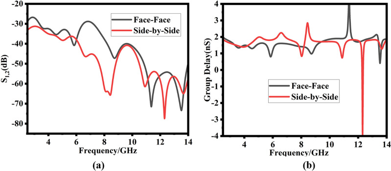
Time-domain analysis is one of the important considerations for the proposed design performance validation. In UWB technology, the transmitting and receiving signals are narrow pulses that suffer from dispersion and distortion due to multi-path and channel losses. Additional important parameters such as transmission coefficient and group delay are required to quantify such effects. To create far-field conditions, twin antennas are oriented face-to-face and side-by-side at a distance of 240 mm (24 cm, two times of ), as shown in Fig. 14a,b, respectively. Both antennas are excited using a Gaussian pulse of 5th order, as follows30.
| 11 |
Fig. 14.
Simulated results of the proposed UWB CP DRA: (a) transmission coefficient (b) group delay.
where t, A, and s stand for time, amplitude, and Gaussian spread pulse, respectively. Figure 14a,b show the simulated magnitude of the forward transmission coefficient and group delay, respectively. As shown in Fig. 14a, the forward transmission coefficient of both orientations is below dB throughout the operating bandwidth except for the pt at 6.5-of 2 GHz, where S12 is lower than dB. Importantly, the S12 value at 10.5–14 GHz has attained a good value of dB. Similarly, Figure 14b shows the simulated group delay for face-to-face and side-by-side orientations. It is observed that group delay showed stable results of approximately 1.5 ns and 2 ns for face-to-face and side-by-side orientations, respectively. Thus, it can be concluded that the proposed antenna design has linear features with smaller S12 values and stable group delay over the entire bandwidth. These characteristics enhance the proposed design potential and suitability for its real-time application.
MIMO parameters
This section evaluates the MIMO and diversity characteristics of the proposed antenna by calculating key MIMO parameters like the envelope correlation coefficient (ECC), diversity gain (DG), channel capacity loss (CCL), and total effective reflection coefficient (TARC).
Envelop correlation coefficient
The ECC is a crucial parameter in MIMO antenna systems since it gauges the isolation or correlation between the different communication branches. The ECC is calculated using (8) and (9) by utilizing the far-field radiation patterns of the proposed MIMO antenna31. For perfect isolation between the elements, the ECC value is ideally considered zero however, for practical applications, a value below 0.5 is sufficient to provide a high level of diversity performance31.
| 12 |
In (8), is the radiation pattern in terms of vector function , represents the spherical angles (elevation, azimuth), and are complex functions.
| 13 |
Figure 15 displays the ECC simulation and measurement outcomes of the proposed design. The maximum value is 0.001, a very low figure that spans a large section of the operational bandwidth with values nearly equal to zero. This smaller value indicates that in real-world MIMO communication systems, the MIMO channels will essentially be independent when using the proposed MIMO antenna array layout.
Fig. 15.
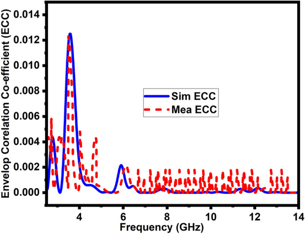
Simulated and measured ECC of the proposed design.
Diversity gain
The assessment of signal quality improvement achieved by diversity approaches is the main goal of DG computation. Figure 16 shows the proposed MIMO antenna measured and simulated DG. The figure shows that DG is roughly 10 dB throughout the operating bandwidth. This high value of diversity gain validates the various MIMO antenna functions of the proposed design. Enhancing signal robustness and reliability, the resulting DG shows how well the recommended antenna design functions in MIMO communication systems31.
| 14 |
Fig. 16.
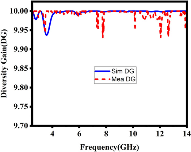
Simulated and measured DG of the proposed design.
Total active reflection coefficient (TARC)
The TARC is an additional parameter utilized to quantify MIMO diversity. TARC determines a MIMO antenna system’s effective operational bandwidth. The TARC of a two-port MIMO antenna, in which N represents the number of ports, represents the angle of observation, which varies from 0 to 2. where reflection and transmission coefficient is represented by S, depending on subscript31, can be expressed as
| 15 |
The TARC needs to be below 0 dB in a MIMO antenna system to improve communication. The TARC response of the suggested MIMO design is illustrated in Fig. 17, which varies the value of from at an interval of . This demonstrates that the adjustments in the feed phase difference have a negligible impact on the resonance behavior of the suggested prototype.
Fig. 17.
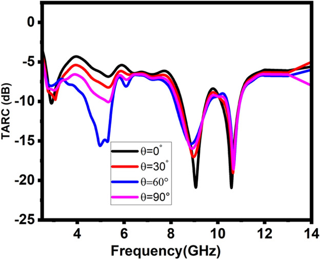
Shows the proposed design simulated TARC.
Channel capacity loss (CCL)
The CCL is another important diversity performance metric that is utilized in the process of analyzing the performance of MIMO antenna systems. The term can be described as the data transmission rate across a certain channel in a fading environment for an effective performance from the MIMO antenna. CCL can be computed as follows31. As illustrated in Fig. 18, the suggested designs have a CCL value < 0.4 bits/sec/Hz, ensuring the high throughput of the proposed 2-port MIMO system.
| 16 |
Where is the correlation matrix at the receiving antenna.
| 17 |
| 18 |
| 19 |
Figure 18, presenting simulated CCL, demonstrates the design’s robust performance across the UWB spectrum, with a slight exception noted at 4 GHz. Although there is a decline in CCL performance at this frequency, the value remains well within acceptable limits for real-time applications.
Fig. 18.
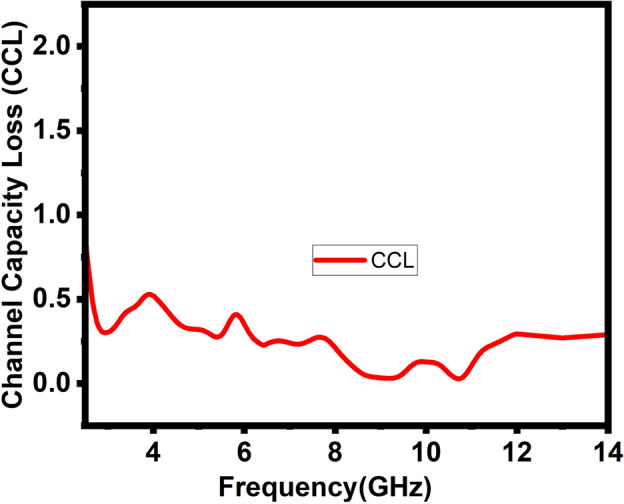
Simulated CCL of the proposed design.
Link budget analysis
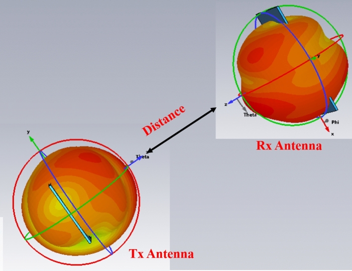
UWB technology is highly preferred in short-range communication due to wide bands and high data rates. Unfortunately, the reflection and diffraction of electromagnetic waves cause multipath fading problems, which affect the antenna’s overall performance. It is, therefore, important to test the designed antenna performance in a free-space virtual line-of-sight (LOS) environment, as shown in Fig. 19. In this experimental setup, the transmitting (TX) antenna remains fixed, while the receiving (RX) antenna is continuously moved from 100 centimeters to 50 meters. Because of this displacement, it is possible to investigate the path loss phenomenon, which ultimately helps evaluate the link budget for the proposed design31.
Fig. 19.
Link budget estimation for VLOS environment of proposed MIMO system.
A link margin with values greater than 0 indicates effective and reliable wireless communication32. The link margin is the difference between the received power and available power. The received power by the receiving antenna is obtained as
| 20 |
Where, represents the energy-to-noise ratio for single-bit transmission, the symbol K represents the Boltzmann constant, whereas T represents Kelvin’s temperature, which is assumed to be 290. As given in equation 18, BR refers to the data transfer rate the communication link can sustain while maintaining a minimal link margin33.
| 21 |
The link budget is mathematically represented by equation (18)34
| 22 |
Where FSPL denotes free space path loss, denotes MIMO antenna system gain where are the other losses that are not considered explicitly. In the NLOS scenario, the analysis gets more complicated as a result of obstacles and reflection. The equation that describes the NLOS link budget is given in (19)35:
| 23 |
Where is an extra loss due to obstacles and NLOS conditions.
The link budget estimation over varied bit rates of the proposed MIMO antenna system is calculated at 2.8 GHz, 4.2 GHz, 5.523 GHz, 8.9 GHz, and 10.7 GHz. Figure 20a shows LOS communication, where the path loss exponent (n) is 1.5. Decreasing the data rates to 0.1 Gbps enhances the link margin. It is essential to note that for all the data rates, the LOS communication coverage distance is more than 80 m for a link margin of 20 dB. Figure 20b shows free space communication with path loss exponent 2. It is observed that with a bit rate of 5 Gbps and a 20 dB link margin, a reliable communication link can be established for a distance up to around 35 m. Moreover, at a reduced bit rate of 2 Gbps, communication is enhanced to 55 m. Further, reducing the data rate to 0.1 Gbps for free space communication increases the communication distance by more than 80 m. For NLOS communication, the link budget estimation is shown in Fig. 20c. it is clear from the figure that for a bit rate of 5 Gbps and 2 Gbps, data transfer between the Tx and Rx is possible up to 15 m and 18 m, respectively. Further reducing the bit rate to 0.1 Gbps makes the data transfer possible to 40 m.
Fig. 20.
Link budget estimation at 2.8 GHz.
Figure 21 represents link budget analysis at 4.2 GHz, where the MIMO design is circularly polarized. The LOS communication for path loss exponent of 1.5 is shown in Fig. 20a; the possible communication distance for 5 Gbps is 35 m, while for a reduced bit rate of 2 Gbps, the data transfer rate is increased to 55 m distance for the 20 dB link margin. For a bit rate of 0.1Gbps, the communication is possible to over 80 m. Figure 21b explains the link margin for accessible space communication with a path loss exponent of 2. For a bit rate of 5 Gbps, data transfer is possible for a short distance of 15 m. Decreasing the bit rate by 2 Gbps enhances the communication distance up to 25 m. NLOS communication with path loss exponent three is presented in Fig. 21c. It is seen that a bit rate of 5 Gbps supports a 5 m distance, a 2 Gbps data rate supports up to 8 m, and 0.1 Gbps supports up to 25 m distance.
Fig. 21.
Link budget estimation at 5.04 GHz.
The link budget estimation for the proposed design is also analyzed at 5.523 GHz, as shown in Fig. 22. Figure 22a demonstrates that for LOS communication at 5 Gbps, the proposed design supports communication up to 30 m, with a further decrease in the data rate to 2Gbps, the communication is feasible across a distance of 40 m for a 20 dB link margin. For a 0.1 Gbps bit rate, the communication distance is increased to more than 80 m. Figure 22b explains the link margin for accessible space communication at 5.523 GHz. For a bit rate of 5 and 2 Gbps, the communication distance is 15 and 20 m, respectively. However, for 0.1 Gbps, the communication distance is enhanced to 80 m. Figure 22c displays the non-line-of-sight (NLOS) link margin. As shown in the figure, for a 20 dB link margin, at 5 and 2 Gbps, the maximum communication distances are 5 and 8 m, respectively. Figure 23 elucidates the link budget estimation at 8.9 GHz, showcasing a behavior consistent with other frequencies, albeit with variations in communication ranges for varying bit rates.
Fig. 22.
Link budget estimation at 5.523 GHz.
Fig. 23.
Link budget estimation at 8.9 GHz.
Figure 24 describes details of the link budget estimation for the proposed design at 10.7 GHz. At this frequency, the design has relatively low simulated and measured gains. This impact is reflected in all three scenarios. Considering the different bit rates, there is a decrement in communication distance for all three cases.
Fig. 24.
Link budget estimation at 10.7 GHz.
A detailed comparison between the proposed design and recently published research works is detailed in Table 4. The comparison is mainly based on physical and electrical lengths, operating bandwidth, axial ratio bandwidth, mutual coupling, and gain. The comparison table confirms the dominant performance of the proposed design compared to published works in that it is compact regarding DR physical and electrical lengths. The design offers a wider operating band with a good CP performance. Moreover, it also provides high MIMO performance in terms of ECC, DG, CCL, and TARC. The detailed link budget analysis also shows the proposed design’s effectiveness in data rate by increasing the distance between the transmitter and receiver. The proposed design covers X-band, C-band, UW band and a part of S-band. With this much compactness, high data rates, wideband response and CP features, the proposed design is a good candidate of short range communication, satellite and C-band application. With these performance parameters, it can also be equally useful for IoT and microwave medical imaging (brain tumor and breast cancer detection).
Table 4.
Comparison of antenna sizes, operating bands, and other features.
| References | 36 | 37 | 38 | 39 | 40 | 41 | 42 | 43 | 44 | 45 | This work |
|---|---|---|---|---|---|---|---|---|---|---|---|
| Size (mm2) | 9549.71.6 | 44451.6 | 50500.762 | 80801.6 | 30251.6 | 31.527.5x0.76 | 105541.6 | 26260.75 | 40400.8 | 66.3 401.6 | 50901.6 |
| (10.50.018) | (0.750.770.02) | (0.60.60.015) | (1.11.10.03) | (0.30.270.017) | (0.3030.260.007) | (1.640.840.025) | (0.320.320.01) | (0.460.460.18) | 0.8 0.50.02 | (0.40.750.013) | |
| DR size (mm3) | 181820 | 313111 | 121210 | 1065 | 1518.56 | 23.419.225.78 | 168 | 201212 | 20.820.815.5 | 21.521.510 | 20105 |
| (0.15 0.15 0.21) | (0.220.220.18) | (2.95.8914.4) | (0.140.060.07) | (0.160.20.06) | (0.220.080.24) | (0.950.123) | (0.240.250.25) | (0.180.180.13) | 0.270.270.12 | (0.160.080.04) | |
| Operating band (GHz) | 3.15-3.93 | 5.18–5.62 | 4.24–4.57 | 5.71–8.20 | 3.3-10.8 | 2.89-5.95 | 4.7–6.4 | 3.71–7.4 | 2.67–4.27 | 3.8 -4.2 | 2.5 – |
| (%) | (24.7) | (8.4) | (7.7) | (37) | (125) | (69.23) | (30.9) | (66.8) | (46.1) | 10 | (133) |
| Axial ratio | 3.34–4.02 | 5.2–5.68 | 4.29–6.72 | 7.72-8.04 | NA | 3.71-5.82 | 4.5–5.7 | 3.72-6.53 | 3.08–3.88 | 3.79-4.9 |
SISO 3.6–4.8 , 9.3–10.1 MIMO (3.9–4.4) |
| AR bandwidth (%) | 18.5 | 8.82 | 44.14 | 4.55 | NA | 44.8 | 23.52 | 54.8 | 23 | 6.8 | 33, 8.6, 12.8 |
| UWB | |||||||||||
| MIMO | |||||||||||
| Gain (dBi) | 4.6 | 2.1 | 3.8 | 6.34 | 10 | 4.6 | 5.4 | 5 | 5.04 | ||
| Isolation (dB) | 15 | 15 | 20 | 46 | |||||||
| Link budget analysis | No | No | No | No | No | No | No | No | No | No | Yes |
Conclusion
A low profile, wideband, circularly polarized, highly compact, and high-isolation MIMO DRA for UWB application is developed and thoroughly investigated. A DR with an extended feedline and a truncated ground plane with a hook-shaped stub has been incorporated, generating a wide impedance bandwidth with better impedance matching, having two CP bands for SISO arrangement, and one CP band for MIMO arrangement. Without any additional decoupling techniques, the orthogonal orientation of the MIMO design has kept the mutual coupling below 45 dB over 12.5 GHz fractional bandwidth. The fabricated design has validated the simulated results with 5.5 dBi measured peak gain, 12.6 GHz measured fractional bandwidth, 9.99 dB peak measured diversity gain, and 0.01 ECC. The low CCL, TARC, and excellent link budget results confirm the effectiveness of the proposed design for the UWB application.
Acknowledgements
The authors would like to thank Dassault Systemes, France, for making CST Microwave Studio available. This work is partially supported by the National Science Centre of Poland Grant 2020/37/B/ST7/01448, by the Nobelium Joining Gdansk Tech Research Community DEC-17/2021/IDUB/I.1, and by the Icelandic Research Fund Grant 2410297.
Author contributions
S. Khan, O. Khan, and S. Koziel implemented the invented research idea and analyzed the data and results. S. A. A. Shah, B. T. Malik, and N. Gohar supervised the work and helped with article write-up, review, and drafting. S. Koziel financially supported the study. All authors reviewed the manuscript.
Data availability
The datasets used and/or analyzed during the current study are available from the corresponding author upon reasonable request.
Footnotes
Publisher’s note
Springer Nature remains neutral with regard to jurisdictional claims in published maps and institutional affiliations.
Contributor Information
Shahid Khan, Email: shahid.khan@pg.edu.pl.
Slawomir Koziel, Email: koziel@ru.is.
References
- 1.Gu, L., Yang, W., Liao, S., Xue, Q. & Che, W. Novel coupling cancellation method by loading planar path for wideband high-isolation wide-scanning millimeter-wave phased array. IEEE Trans. Antennas Propag.70, 10520–10530 (2022). [Google Scholar]
- 2.Sun, L., Li, Y. & Zhang, Z. Decoupling between extremely closely spaced patch antennas by mode cancellation method. IEEE Trans. Antennas Propag.69, 3074–3083 (2020). [Google Scholar]
- 3.Lai, Q. X., Pan, Y. M. & Zheng, S. Y. A self-decoupling method for mimo antenna array using characteristic mode of ground plane. IEEE Trans. Antennas Propag.71, 2126–2135 (2023). [Google Scholar]
- 4.Jafargholi, A., Jafargholi, A. & Choi, J. H. Mutual coupling reduction in an array of patch antennas using cll metamaterial superstrate for mimo applications. IEEE Trans. Antennas Propag.67, 179–189 (2018). [Google Scholar]
- 5.Liu, F. et al. Dual-band metasurface-based decoupling method for two closely packed dual-band antennas. IEEE Trans. Antennas Propag.68, 552–557 (2019). [Google Scholar]
- 6.Dadgarpour, A., Zarghooni, B., Virdee, B. S., Denidni, T. A. & Kishk, A. A. Mutual coupling reduction in dielectric resonator antennas using metasurface shield for 60-ghz mimo systems. IEEE Antennas Wirel. Propag. Lett.16, 477–480 (2016). [Google Scholar]
- 7.Luo, C.-M., Hong, J.-S. & Zhong, L.-L. Isolation enhancement of a very compact uwb-mimo slot antenna with two defected ground structures. IEEE Antennas Wirel. Propag. Lett.14, 1766–1769 (2015). [Google Scholar]
- 8.Su, S.-W., Lee, C.-T. & Chang, F.-S. Printed mimo-antenna system using neutralization-line technique for wireless usb-dongle applications. IEEE Trans. Antennas Propag.60, 456–463 (2011). [Google Scholar]
- 9.Zhang, Y., Deng, J.-Y., Li, M.-J., Sun, D. & Guo, L.-X. A mimo dielectric resonator antenna with improved isolation for 5g mm-wave applications. IEEE Antennas Wirel. Propag. Lett.18, 747–751 (2019). [Google Scholar]
- 10.Elahi, M., Joung, J. & Lim, S. Isolation and bandwidth enhancement in compact cp mimo dra in h-plane using z-shaped strip. IEEE Antennas Wirel. Propag. Lett.22(11), 2700–2704 (2023). [Google Scholar]
- 11.Abedian, M. et al. High isolation circularly polarized in-band full-duplex anisotropic dielectric resonator antenna. Sci. Rep.13, 5937 (2023). [DOI] [PMC free article] [PubMed] [Google Scholar]
- 12.Kumar, A. Substrate integrated waveguide cavity-backed slot antenna with low cross-polarization over the full bandwidth. Microw. Opt. Technol. Lett.66, e34019 (2024). [Google Scholar]
- 13.Chaturvedi, D., Kumar, A. & Althuwayb, A. A. A dual-band dual-polarized siw cavity-backed antenna-duplexer for off-body communication. Alex. Eng. J.64, 419–426 (2023). [Google Scholar]
- 14.Chaturvedi, D. & Kumar, A. A qmsiw cavity-backed self-diplexing antenna with tunable resonant frequency using csrr slot. IEEE Antennas and Wireless Propagation Letters (2023).
- 15.Gaya, A., Jamaluddin, M. H., Alali, B. & Althuwayb, A. A. A novel wide dual band circularly polarized dielectric resonator antenna for milli meter wave 5g applications. Alex. Eng. J.61, 10791–10803 (2022). [Google Scholar]
- 16.Anuar, S. U. et al. Triple band mimo dielectric resonator antenna for lte applications. AEU-Int. J. Electron. Commun.118, 153172 (2020). [Google Scholar]
- 17.Sahu, N. K., Das, G. & Gangwar, R. K. Circularly polarized offset-fed dra elements & their application in compact mimo antenna. Eng. Sci. Technol. Int. J.28, 101015 (2022). [Google Scholar]
- 18.Patri, U. & Kumar, A. A novel ultra wideband circularly polarized stacked cylindrical dielectric resonator antenna with modified ground plane. Int. J. RF Microwave Comput. Aided Eng.32, e23221 (2022). [Google Scholar]
- 19.Iqbal, A., Bouazizi, A., Kundu, S., Elfergani, I. & Rodriguez, J. Dielectric resonator antenna with top loaded parasitic strip elements for dual-band operation. Microw. Opt. Technol. Lett.61, 2134–2140 (2019). [Google Scholar]
- 20.Illahi, U. et al. Design and development of a singly-fed circularly polarized rectangular dielectric resonator antenna for wimax/satellite/5g nr band applications. AEU-Int. J. Electron. Commun.126, 153443 (2020). [Google Scholar]
- 21.Elahi, M., Altaf, A., Yang, Y., Lee, K.-Y. & Hwang, K. C. Circularly polarized dielectric resonator antenna with two annular vias. IEEE Access9, 41123–41128 (2021). [Google Scholar]
- 22.Lai, Q. X., Pan, Y. M. & Zheng, S. Y. A self-decoupling method for mimo linear and planar dielectric resonator antenna arrays based on transmission c haracteristics of feeding structure. IEEE Trans. Antennas Propag.71(7), 5708–5716 (2023). [Google Scholar]
- 23.Sani, M. M., Chowdhury, R. & Chaudhary, R. K. An ultra-wideband rectangular dielectric resonator antenna with mimo configuration. IEEE Access8, 139658–139669 (2020). [Google Scholar]
- 24.Chen, H. N., Song, J.-M. & Park, J.-D. A compact circularly polarized mimo dielectric resonator antenna over electromagnetic band-gap surface for 5g applications. IEEE Access7, 140889–140898 (2019). [Google Scholar]
- 25.Roshna, T., Deepak, U., Sajitha, V., Vasudevan, K. & Mohanan, P. A compact uwb mimo antenna with reflector to enhance isolation. IEEE Trans. Antennas Propag.63, 1873–1877 (2015). [Google Scholar]
- 26.Kumar, R., Thummaluru, S. R. & Chaudhary, R. K. Improvements in wi-max reception: A new dual-mode wideband circularly polarized dielectric resonator antenna. IEEE Antennas Propag. Mag.61, 41–49 (2019). [Google Scholar]
- 27.Naeem, U., Iqbal, A., Shafique, M. F. & Bila, S. Efficient design methodology for a complex dra-siw filter-antenna subsystem. Int. J. Antennas Propag.2017, 6401810 (2017). [Google Scholar]
- 28.Sarfraz, H. et al. Next-generation multiband wireless systems: A compact cssr-based mimo dielectric resonator antenna approach. IEEE Access (2023).
- 29.Koc Polat, H., Geyikoglu, M. D. & Cavusoglu, B. Modeling and validation of a new reconfigurable patch antenna through equivalent lumped circuit-based design for minimum tuning effort. Microw. Opt. Technol. Lett.62, 2335–2345 (2020). [Google Scholar]
- 30.Kumari, R. & Gangwar, R. K. Circularly polarized slot-coupled square dielectric resonator antenna for wlan applications. Microw. Opt. Technol. Lett.60, 2787–2794 (2018). [Google Scholar]
- 31.Raheel, K. et al. Design and performance evaluation of orthogonally polarized corporate feed mimo antenna array for next-generation communication system. IEEE Access (2024).
- 32.Shah, S. A. A., Lim, Y.-H. & Yoo, H. A novel development of endovascular aortic stent system featuring promising antenna characteristics. IEEE Trans. Antennas Propag.70, 2214–2222 (2021). [Google Scholar]
- 33.Shah, S. A. A., Basir, A., Lim, Y.-H. & Yoo, H. A novel efficient wirelessly powered biotelemetric endovascular aortic stent antenna system. IEEE Transactions on Antennas and Propagation (2023).
- 34.Shariff, B. P. et al. High-isolation wide-band four-element mimo antenna covering ka-band for 5g wireless applications. IEEE Access (2023).
- 35.Kiourti, A. & Nikita, K. S. Miniature scalp-implantable antennas for telemetry in the mics and ism bands: Design, safety considerations and link budget analysis. IEEE Trans. Antennas Propag.60, 3568–3575 (2012). [Google Scholar]
- 36.Chen, H. N., Song, J.-M. & Park, J.-D. A compact circularly polarized mimo dielectric resonator antenna over electromagnetic band-gap surface for 5g applications. IEEE Access7, 140889–140898 (2019). [Google Scholar]
- 37.Kumari, R. & Gangwar, R. K. Circularly polarized slot-coupled square dielectric resonator antenna for wlan applications. Microw. Opt. Technol. Lett.60, 2787–2794 (2018). [Google Scholar]
- 38.Dash, S. K. K., Khan, T. & Kanaujia, B. K. Circularly polarized dual facet spiral fed compact triangular dielectric resonator antenna for sensing applications. IEEE Sens. Lett.2, 1–4 (2018). [Google Scholar]
- 39.Varshney, G., Singh, R., Pandey, V. S. & Yaduvanshi, R. S. Circularly polarized two-port mimo dielectric resonator antenna. Progr. Electromagn. Res. M91, 19–28 (2020). [Google Scholar]
- 40.Kumari, P., Gangwar, R. K. & Chaudhary, R. K. An aperture-coupled stepped dielectric resonator uwb mimo antenna with amc. IEEE Antennas Wirel. Propag. Lett.21, 2040–2044 (2022). [Google Scholar]
- 41.Trinh-Van, S., Yang, Y., Lee, K.-Y. & Hwang, K. C. Single-fed circularly polarized dielectric resonator antenna with an enhanced axial ratio bandwidth and enhanced gain. IEEE Accessd8, 41045–41052 (2020). [Google Scholar]
- 42.Gupta, S., Sharma, A., Das, G., Gangwar, R. K. & Khalily, M. Wideband circularly polarized dielectric resonator antenna array with polarization diversity. IEEE Access7, 49069–49076 (2019). [Google Scholar]
- 43.Abedian, M. et al. Novel wideband circularly polarized dra with squint-free radiation characteristics. Sci. Rep.11, 7198 (2021). [DOI] [PMC free article] [PubMed] [Google Scholar]
- 44.Wang, C. et al. A wideband circularly polarized dielectric resonator antenna with flat gain response within the passband. AEU-Int. J. Electron. Communi.177, 155224 (2024). [Google Scholar]
- 45.Dwivedi, A. K., Sharma, A., Singh, A. K. & Singh, V. Metamaterial inspired dielectric resonator mimo antenna for isolation enhancement and linear to circular polarization of waves. Measurement182, 109681 (2021). [Google Scholar]
Associated Data
This section collects any data citations, data availability statements, or supplementary materials included in this article.
Data Availability Statement
The datasets used and/or analyzed during the current study are available from the corresponding author upon reasonable request.


