Abstract
Ternary metal carbide TiAlC has been proposed as a metal gate material in logic semiconductor devices. It is a hard-to-etch material due to the low volatility of the etch byproducts. Here, a simple, highly controllable, and dry etching method for TiAlC has been first presented using nonhalogen N2/H2 plasmas at low pressure (several Pa) and 20 °C. A capacitively coupled plasma etcher was used to generate N2/H2 plasmas containing active species, such as N, NH, and H to modify the metal carbide surface. The etch rate of TiAlC was obtained at 3 nm/min by using the N2/H2 plasma, whereas no etching occurred with pure N2 plasma or pure H2 plasma under the same conditions. The surface roughness of the TiAlC film etched by N2/H2 plasma was controlled at the atomic level. A smooth etched surface was achieved with a root-mean-square roughness of 0.40 nm, comparable to the initial roughness of 0.44 nm. The plasma properties of the N2/H2 plasmas were diagnosed by using a high-resolution optical emission spectrometer, detecting the NH molecular line at 336 nm. The etching behavior and plasma–surface reaction between N2/H2 plasma and TiAlC were investigated by using in situ spectroscopic ellipsometry, in situ attenuated total reflectance-Fourier transform infrared spectrometry, and X-ray photoelectron spectroscopy. The findings indicate that the N–H, C–N, and Ti(Al)–N bonds form on the TiAlC surface etched by the N2/H2 plasmas. The mechanism for etching of TiAlC involving transformation reactions between inorganic materials (metal carbides) and inorganic etchants (N2/H2 plasma) to form volatile organic compounds such as methylated, methyl-aminated, and aminated metals is proposed. Nonhalogen or nonorganic compound etchants were used during the etching process. The study provides useful insights into microfabrication for large-scale integrated circuits.
Keywords: metal carbide, TiAlC, metal compound etching, nonhalogen dry etching, N2/H2 plasma, plasma-surface reaction
1. Introduction
Metal carbides (TiC and TiAlC) and metal nitrides (TiN, TaN, AlN, and TiAlN) have been proposed to be used as metal gate materials in a logic semiconductor device.1−4 Ternary metal compound TiAlC belongs to high-melting point, high-hardness, and high-wear resistance materials.1,5 TiAlC is a hard-to-etch material, and the conventionally wet etching of Ti compounds using H2O2 mixtures causes poor etching performance and device damage.6 In advanced fabrication of the next-generation fin-type or nanosheet field effect transistor of 3D multilayer semiconductor devices, it is strongly demanded to develop a dry etching method that enables a high controllability and high reproducibility of etchant species and their energies as well as high selectivity between metal compounds for both isotropic and anisotropic applications. Plasma etching is a dry method that meets these requirements and has been widely applied to a variety of materials.7−9
In general, dry etching of metals or metal compounds requires halogen etchants or complicated cyclic process including surface modification (oxidation, fluoridation, or chlorination) and removal of the modified layer by organic compounds (formic acid, acetylacetone, or hexafluoroacetylacetone) or subsequences of ligand exchange with the support of accelerating substrate temperature, up to several hundred degrees due to low volatility of the modified layer at room temperature.10−12 The traditional etchants used for plasma etching are halogen-based gases. TiC etching was studied using fluorine-containing (CF4, CHF3, and SF6) high-density plasmas.13 Al2O3–TiC etching in halogen-based plasmas such as fluorine-containing (CF4 and SF6) plasmas14 and chlorine-containing (Cl2/BCl3/Ar) high-density plasmas15,16 was investigated; however, the difference in etch rates of Al2O3 and TiC grains in the substrate results in the rough-etched morphologies. To find reasonable etchants for new materials, predicting volatile products for etching metal compounds is indispensable. Fluorine-based plasma is not suitable for etching Al-based compounds due to the formation of a nonvolatile product [AlF3, boiling point (bp) more than 1290 °C].16,17 Chlorine-based plasmas can form volatile products with TiAlC, such as TiCl4 (bp ∼136 °C) and AlCl3 (bp ∼183 °C).18 Nonhalogen etchants for etching of Ti compounds were proposed in our previous study, in which a feasible dry etching method for ternary material TiAlC using a wet-like plasma generated from a floating wire (FW)-assisted high-density vapor plasma of Ar gas mixed with a liquid vapor source of NH4OH-based mixtures at medium pressure was demonstrated.19 By using this high-density plasma source,20−22 a generated rich radical source (1014 cm–3) can produce a large amount of etchant or coreactant species to enhance the reaction rate with the sample surface. The results indicate that species such as N, NH, and H radicals play a key role in surface modification and etching of TiAlC.
In this study, low-pressure dry etching of the ternary material TiAlC has been first presented using plasmas generated from nonhalogen and noncorrosive N2/H2 gas mixtures, where the ratio between N2 and H2 can be easily controlled. A capacitively coupled plasma (CCP) etcher was used to generate N2/H2 plasmas at several Pa. The substrate temperature was controlled at 20 °C. The etch rate of TiAlC was around 3 nm/min using the N2/H2 plasma, whereas no etching occurred using only N2 plasma or H2 plasma. The surface roughness of the TiAlC film etched by N2/H2 plasma can be controlled at the atomic level. A smooth etched surface was achieved with a root-mean-square roughness (rms) of 0.40 nm, comparable to the initial roughness of 0.44 nm. The plasma properties of N2/H2 plasmas were diagnosed using a high-resolution optical emission spectrometer (HR-OES) with detection of the NH molecular line at 336 nm. The etching behavior and plasma–surface reaction between N2/H2 plasma and TiAlC were investigated by using in situ spectroscopic ellipsometry, in situ attenuated total reflectance-Fourier transform infrared spectrometry (ATR-FTIR), and X-ray photoelectron spectroscopy (XPS). The findings indicate the formation of N–H, C–N, and Ti(Al)–N bonds on the TiAlC surface during the N2/H2 plasma exposure. To predict volatile products, density functional theory (DFT) was employed to model organometallic molecules using the Gaussian 16 program.23 Methylation, methylamination, amination, and hydrogenation of the TiAlC film can be obtained by controlling the active species such as N, NH, and H. The mechanism for etching ternary metal carbide TiAlC by N2/H2 plasma, based on both chemical reactions and physical sputtering through transformation reactions between an inorganic material (metal carbide) and an inorganic etchant (N2/H2 plasma) to form volatile organic compounds, is proposed here.
2. Experimental Procedures
2.1. Plasma Discharges for Etching
A CCP etcher was used to generate N2/H2 plasmas, and the upper and lower electrodes were operated with 100 and 2 MHz sources, respectively. Figure 1 shows the schematic of the CCP etcher with an in situ spectroscopic ellipsometer for real-time measurement and an in situ ATR-FTIR spectrometer.
Figure 1.
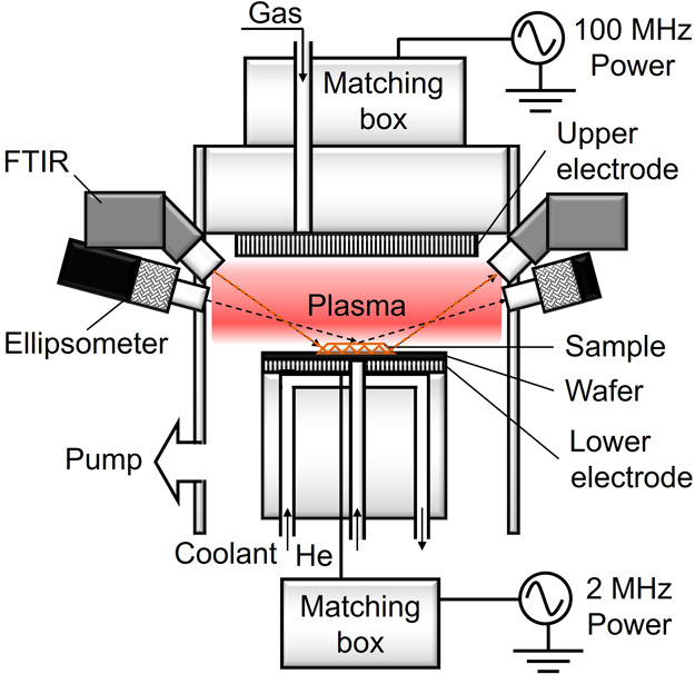
Schematic of the CCP etcher with an in situ spectroscopic ellipsometer for real-time measurement and an in situ ATR-FTIR spectrometer.
The samples (15 mm × 20 mm) were fixed on a 100 mm Si carrier wafer placed on the lower electrode with an electrostatic chuck. To improve the thermal conductivity between the chuck and wafer, a He backflow was controlled at a pressure around 600–700 Pa. The distance between the top electrode and the sample surface during the plasma discharge is 30 mm, and that between the top electrode and the sample surface for the ATR-FTIR measurement is 90 mm. To fix the sample on Si wafer, fluorinated grease with high chemical stability at low vapor pressure and a temperature range of −70 to 200 °C was used. The background vacuum pressure was around 5–6 × 10⁻⁴ Pa before plasma exposure. The substrate temperature was controlled at 20 °C with a coolant circulator. Details of the process parameters for plasma etching condition are presented in Table 1, where Vpp represents the plasma potential.
Table 1. Plasma Etching Condition.
| N2/H2 gas mixture ratio dependence | |||||
|---|---|---|---|---|---|
| excitation power (W) | 300 | ||||
| bias power (W) | 200 | ||||
| substrate temperature (°C) | 20 | ||||
| working pressure (Pa) | 4 | ||||
| N2/H2 flow rate (sccm/sccm) | 150/0 | 100/50 | 75/75 | 50/100 | 0/100 |
| H2 % | 0.00 | 33.33 | 50.00 | 66.67 | 100.00 |
| Vpp (V) | 1500 | 1265 | 1255 | 1255 | 1210 |
| working pressure (Pa) | 2 | ||||
| N2/H2 flow rate (sccm/sccm) | 100/0 | 75/25 | 50/50 | 25/75 | 0/100 |
| H2 % | 0 | 25 | 50 | 75 | 100 |
| Vpp (V) | 1410 | 1260 | 1260 | 1240 | 1210 |
In this study, the excitation power and bias power were fixed at 300 W and 200 W, respectively. The working pressure was controlled at 4 and 2 Pa. H2 % is defined as the H2 volume percentage in total of volume of N2 gas and H2 gas mixture [H2/(N2 + H2) %]. Various H2 % were controlled from 0% (pure N2 gas) to 100% (pure H2 gas). The values of Vpp was monitored during the plasma process.
2.2. Plasma Diagnostics
The OES of the N2/H2 plasmas were detected by using a spectrometer (Ocean Photonics, HR4000CG-UV-NIR) with the wavelength from 200 to 900 nm. It was observed through a quartz window on the chamber wall and was directed toward the center between two electrodes. The exposure time was set to maximize the intensity (best resolution), so it was set at 40 and 20 ms for the respective working pressures of 4 and 2 Pa because the maximum intensity at 2 Pa is much higher than that at 4 Pa. The number of accumulations for all of measurements by using this OES was set at 3.
The emission of NH (336.00 nm) was detected by a HR-OES. A computer-controlled Acton 750 monochromator equipped with an intensified charge-coupled device (ICCD) detector (Andor DH734-18U-03) was used to provide a spectral resolution of about 0.007 nm at gratings of 2400 groove mm–1. The spectral resolution here is defined by the distance between two measured continuous wavelength points. The center wavelength for this measurement is set at 337.13 nm that is the band head of N2 second positive system (SPS) (0,0).24 The number of accumulations for all of the measurements by using the HR-OES was set at 20. A slit size of the ICCD detector was set at 20 μm.
2.3. Material Preparation and Characterization
The pristine TiAlC films were prepared on Si wafer by a radio frequency reactive ion plating process with Ti and Al sources and C2H2 gas. 40 nm TiAlC film/Si samples were prepared with the size of 15 mm × 20 mm. For ATR-FTIR spectrometry measurement, the 10 nm TiAlC film was deposited on germanium (Ge) trapezoid prism with the same conditions, as deposited on a Si wafer. The Ge prism had a dimension of 52 mm × 20 mm, a thickness of 2 mm, and an angle of 45° for the bevel edges.
The crystalline structure of the pristine TiAlC sample was evaluated by a high-resolution double-crystal X-ray diffractometer (HRXRD, 9 kW Rigaku Smartlab diffractometer, Rigaku Co. Ltd.) with the arrangement of θ–2θ using Bragg-Brentano geometry. The radiation source was from CuKα (1.542 Å), and the scan step was set at 0.02°/step. The XRD pattern of the pristine TiAlC sample used in this study shows that it is a polycrystalline Al-doped TiC (see Supporting Information, Figure S1).
The spectra and composition of the pristine TiAlC sample after removing native oxide were evaluated with an XPS chamber equipped with an Ar sputter at 3 keV and 1 μA to a sputter area of 4 mm × 4 mm for 40 min. The XPS spectra were obtained by using a spectrometer (Ulvac-Phi, XPS 1600) with an Al Kα (photon energy = 1486.6 eV) source in an analysis chamber evacuated down to a base pressure of 7 × 10⁻⁷ Pa. The XPS spectra of pristine TiAlC film before removing native oxide exhibit the chemical bonds such as the Ti–C bond (455.0 eV), Ti–O bond (461.0 eV), Al–Al bond (72.7 eV), Al–C (73.7 eV), and Al–O (75.3 eV) (see Supporting Information, Figure S2a). There is no Ti–Al bond existing in the TiAlC film. After removal of the native oxide (Al–O, Ti–O, C–O, C=O), around 43.4% oxygen in the atomic composition from the surface, the atomic composition ratio of Ti/Al/C/O is around 38:18:35:9 (approximately 4:2:4:1) (see Supporting Information, Figure S2b). Around 9% of oxygen exists inside the TiAlC film.
The film thickness of TiAlC was analyzed by using in situ spectroscopic ellipsometry (M-2000, J.A. Woollam Co.) in real time during the plasma exposure with a Xe arc light source (FLS-300) that can measure the multiwavelength range from 200 to 1000 nm with an incident angle of 75°. The model used for spectral fitting of ellipsometry data of the TiAlC sample was improved from our previous study19 (see Supporting Information, Table S1). Cross-sectional microstructure and thickness of samples were characterized by a cold field-emission scanning electron microscope (FE-SEM, SU-8230, Hitachi).
To analyze the surface modification of the TiAlC, XPS spectra were obtained using a spectrometer (ESCALAB 250, Vacuum Generator, UK) equipped with an Al Kα (photon energy = 1486.6 eV) source that was operated at a pass energy of 20.0 eV and a spot size of 400 μm on the samples. The measurements were performed in a vacuum chamber evacuated to a base pressure of 5 × 10⁻⁷ Pa. Peak deconvolution and elemental concentrations were analyzed by the Advantage program. The calibration was carried out for charge shifting by setting graphitic adventitious C 1s spectrum (C–C peak) to 284.8 eV. Due to good electrical conductivity of the TiAlC samples and the sample fixed with metal clamps, the charge shifts rarely exceeded 0.5 eV.
To evaluate the damage to the surface of TiAlC film etched by N2/H2 plasmas, surface roughness of the TiAlC film was measured by atomic force microscopy (AFM) in Park system (FX40) with noncontact mode for the scan area of 1 μm × 1 μm. The data were analyzed using the Gwyddion program.
2.4. In Situ Monitoring the Structure Modification of the TiAlC Surface by N2/H2 Plasma and IR Spectra Simulation for Prediction of Volatile Products
For confirmation of chemical mechanism and reaction products, IR absorption spectroscopy allows us to determine the local chemical structure of the active surface.25 The change in the chemical bonding structure of the TiAlC surface during the processing was analyzed using an in situ ATR-FTIR system. An IR light source provided by the FTIR system (iS50, Thermo Fisher Scientific) and a liquid-cooled HgCdTe (MCT) detector were used with a resolution of 4 cm–1. The absorbance spectra were taken with the wavenumber ranging from 800 to 4000 cm–1.
To understand experimental spectra and predict volatile products, DFT was used to suggest IR band assignments.25 In this study, the predicted organometallic molecules for volatile products were built using the Gaussian 16 program.23 The molecular structure was optimized at the B3LYP/6-31+G(d,p) level of theory. A homogeneous scaling factor of 0.962 is applied for all simulated spectra to correct of the neglect of anharmonicity.26
3. Results and Discussion
3.1. Etching of TiAlC after Exposing to N2/H2 Plasmas
Depending on the chemistry of the plasma exposure, the etching of TiAlC mainly occurs with N2/H2 plasmas at 4 Pa and 20 °C, as shown in Figure 2. During the N2/H2 plasma (H2 %: 50%) exposure, the thickness of TiAlC decreased 5.45 nm (from 39.96 to 34.51 nm) after the first 5 min exposure and then significantly reduced 13.01 nm (from 34.51 to 21.50 nm) after the second 5 min exposure, indicating that the TiAlC film can be etched by N2/H2 plasma (Figure 2a). In the first 2 min of N2/H2 plasma exposure, native oxide (TiO2 and Al2O3) needs to be removed, so only surface modification occurs instead of etching, after which linear etching can be obtained. To understand the role of N-based or H-based species, the TiAlC film was exposed under pure N2 plasma or pure H2 plasma at the same condition as N2/H2 plasma, and the results show that almost no etching occurs.
Figure 2.
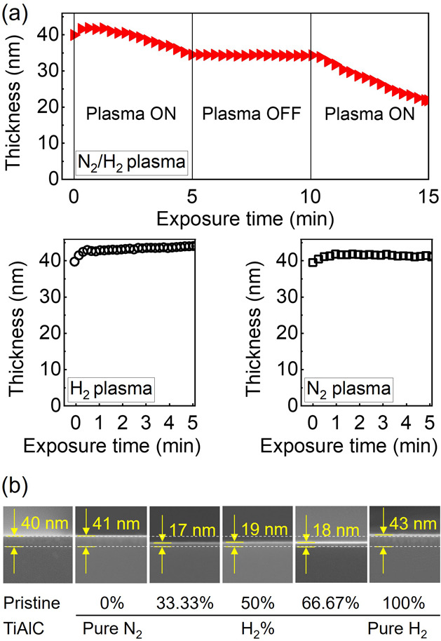
Change of film thickness of the TiAlC film as a function of plasma treatment time by (a) N2/H2 plasma (H2 %: 50%), N2 plasma, and H2 plasma and (b) FE-SEM images of TiAlC at various N2/H2 gas ratios after 10 min plasma exposure. Excitation power: 300 W, bias power: 200 W, working pressure: 4 Pa, and substrate temperature: 20 °C.
During the H2 plasma exposure, the thickness of TiAlC increased from 39.87 to 43.91 nm after 5 min exposure, indicating no etching to the TiAlC surface by H2 plasma. The atomic radii27 and atomic weights28 of the elements used in this study are listed (see Supporting Information, Table S2). The H atom has the smallest atomic radius (1.54 Å) compared to other elements, such as C (1.90 Å), Al (2.39 Å), and Ti (2.57 Å). H ions (H3+ and H+) and H atoms in the pure H2 plasma can be considered as the main reactive species that are easy to deep penetration to the TiAlC film (a significant increase of the thickness of the top layer), possibly leading to the formation of hydrogenated films without becoming volatile products. H2 molecules, H ions, and atoms are supposed to be not efficiently sputter TiAlC because of low-molecular (or atomic) weight, so almost no etching of TiAlC occurs by H2 plasma even though high ion energy was applied (Vpp was approximately 1210 V). TiAlC is a ternary material and contains two metals, Ti and Al. In general, volatilization of metal hydrides during the exposure of metal films to H2 plasmas is difficult, for instance, Cu can be etched by H2 plasmas; however, Ti, Ta, Ni, Cr, and Al are not etched at least under the conditions used to etch Cu, as studied by Choi and Wu et al.29−32
Compared to the hydrogen molecule and atom, the nitrogen molecule and atom exhibit higher molecular (atomic) weight, so it is possible to provide sufficient momentum transfer from N2 plasma to the sample surface.33,34 During the N2 plasma exposure, the thickness of the TiAlC layer slightly increased from 39.79 to 41.21 nm after 5 min exposure, showing a minor sputter effect of N2 plasma to TiAlC even though high ion energy (Vpp was approximately 1500 V) was applied. This implies that forming metal nitrides on the TiAlC surface can be dominant during the N2 plasma exposure, and there is almost no obvious etching effect by both physical sputtering and chemical reaction of N2 plasma with the TiAlC surface.
In comparison with exposure under only pure N2 plasma or pure H2 plasma, etching of TiAlC obviously occurs with the synergy effect from both N ion/atom and H ion/atom in terms of both chemical and physical characteristics. To confirm the etching effect of N2/H2 plasmas on the TiAlC film, the thickness of TiAlC before and after exposure to various N2/H2 plasmas with H2 % ranging from 0% (pure N2) to 100% (pure H2) for 10 min was investigated, as shown in Figure 2b (also see Supporting Information, Table S3). When the TiAlC sample is exposed under H2 plasma or N2 plasma, the thickness of TiAlC before and after plasma exposure is the same 40 nm or higher, indicating that almost no obvious etching effect can be observed in FE-SEM images. When increasing H2 % from 33.33% to 66.67% in the N2/H2 mixtures, the thickness of TiAlC films that could be observed from FE-SEM images (Figure 2b) is around 17–19 nm, indicating an obvious decrease of thickness for all the samples under N2/H2 plasmas exposure.
Figure 3 shows the etch rate of TiAlC at various N2/H2 gas ratios at two working pressures 4 and 2 Pa at the same excitation power of 300 W, bias power of 200 W, and substrate temperature of 20 °C. The etch rate of TiAlC can be achieved higher at lower working pressure. The maximum etch rate of TiAlC for both working pressures 4 and 2 Pa can be obtained at H2 % of around 50% with values of 1.85 and 3.02 nm/min, respectively. With the H2 % less than 33% and higher 67%, the etch rate of TiAlC decreases, indicating that optimizing the N2/H2 ratio is necessary to obtain the greatest etch rate.
Figure 3.
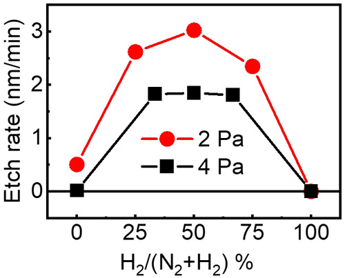
Etch rate of TiAlC at various N2/H2 gas ratios at two working pressures 4 and 2 Pa. Excitation power: 300 W, bias power: 200 W, and substrate temperature: 20 °C. The error bars for the repeated experiments in this figure are smaller than the symbol size.
In addition to the etch rate, H atom penetration to the film is also an important factor because this potentially produces voids in the film. From the FE-SEM and ellipsometry results (Figure 2 and Table S3), the thickness of TiAlC after 10 min H2 plasma exposure increased around 3–6 nm. The optimal percentage of H2 in the N2/H2 gas mixture to obtain the best etch rate and to minimize the H penetration to the TiAlC film can be around 25% to 75%.
3.2. Properties of N2/H2 Plasmas
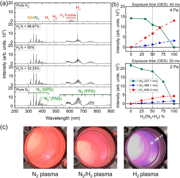
To realize the mechanism of plasma–surface interaction between the N2/H2 plasmas with the surface of TiAlC, the properties of the N2/H2 plasmas are presented here. Figure 4a shows the OES of N2/H2 plasmas at various N2/H2 gas ratios at a working pressure of 4 Pa. The strong emissions of N2 bands such as N2 second positive system SPS (transition C3Πu → B3Πg),35,36 N2+ first negative system FNS,37 and N2 first positive system FPS38 were detected in all of N2-based gas mixture plasmas. The H line emissions were displayed with an increase of the intensity in the order from Hγ (434.1 nm) to Hβ (486.1 nm) and to Hα (656.3 nm).
Figure 4.
(a) Optical emission spectra of N2/H2 plasmas at various N2/H2 gas ratios at the wavelength ranging from 200 to 900 nm at a working pressure of 4 Pa. (b) Relationship between optical emission intensities of N2 (band head at 337.1 nm), Hβ (486.1 nm), and Hα (656.3 nm) of N2/H2 plasmas and various N2/H2 gas ratios at working pressures of 4 and 2 Pa. (c) Photographic images of N2 plasma, N2/H2 plasma, and H2 plasma at 4 Pa. Excitation power: 300 W, bias power: 200 W, working pressure: 4 Pa, and substrate temperature: 20 °C. The error bars in this figure are smaller than the symbol size. SPS: second positive system, FNS: first negative system, and FPS: first positive system.
Figure 4b presents the relationship between optical emission intensities of N2 (band head at 337.1 nm), Hβ (486.1 nm), and Hα (656.3 nm) of N2/H2 plasmas and various N2/H2 gas ratios at working pressures of 4 and 2 Pa. When increasing H2 %, the emissions of both Hβ (486.1 nm) line and Hα (656.3 nm) line gradually increase with higher rate for the intensity of Hα (656.3 nm) line, whereas the emission of N2 (337.1 nm) gradually decreases at H2 % less than 50% and significant decreases after that. The absolute intensity of N2 (337.1 nm) at 2 Pa is almost double in comparison with that at 4 Pa; however, to protect the OES detector, the exposure time was decreased 50% from 40 (4 Pa) to 20 ms (2 Pa). Interestingly, the ratio between the intensity of N2 (337.1 nm) band head and that of Hα at 2 Pa is much higher than the ratio at 4 Pa, for example, at H2 % of 50%, these ratios are 6.18 (2 Pa) and 1.63 (4 Pa), as shown in Table 2.
Table 2. Relationship between the Intensity Ratios of I (N2-337.1 nm)/I (Hα-656.3 nm) and I (N2-337.1 nm)/I (NH-336.0 nm) with the Etch Rate of TiAlCa.
| working pressure | 2 Pa | 4 Pa |
|---|---|---|
| I(N2-337.1 nm)/I (Hα-656.3 nm) | 6.18 | 1.63 |
| I(N2-337.1 nm)/I (NH-336.0 nm) | 4.67 | 4.26 |
| etch rate | 3.02 nm/min | 1.85 nm/min |
H2 %: 50%, excitation power: 300 W, bias power: 200 W, substrate temperature: 20 °C, and plasma exposure time: 10 min.
Figure 4c displays photographic images of N2 plasma, N2/H2 plasma, and H2 plasma at 4 Pa. Depending on the type of plasma, the color gradually changes from orange (N2 plasma) to pink-orange (N2/H2 plasma) and purple (H2 plasma). To produce N, H, and NH reactive species, both NH3 plasma and N2/H2 plasma can be used. NH3 can dissociate by energetic electron collisions to form radicals such as NH2 (571 nm), NH (336 nm), N2 (357 nm), Hβ (486.1 nm), and Hα (656.3 nm).39−41 Very strong NH can be produced from NH3 plasma at both high pressure and low pressure and at both E-mode (low power and capacitive component are dominant) and H-mode (high power and inductive component are dominant) due to the following dissociation19,39
| 1 |
In case of using N2/H2 plasma, depending on the ratio of the N2/H2 mixture, power supply, and working pressure, strong NH optical emission can be detected, for example, from a direct current arc plasma jet at 13.33 kPa and 60% N2/40% H2 gas mixture,41 or is not able to be detected as in the case of using various N2/H2 plasmas at the same working pressure of 13.33 kPa, but using very high-frequency power of 150 MHz.42 The lifetime of the NH2 and NH radicals is very short with less than 10 ms in low-pressure plasma due to the exothermic reactions NH + NH → N2 + H2 (ΔH = −7 eV).43
It is difficult to detect separately the low-intensity NH emission with the N2 emission by the medium-resolution OES system because the optical emission of the NH band is at 336.00 nm [NH (0,0)] that is overlapped by the N2 SPS with the band head at 337.13 nm [N2 (0,0) SPS].24,37,38 To detect the NH emission, the HR-OES system with a spectral resolution of 0.007 nm was used in this study, as shown in Figure 5.
Figure 5.
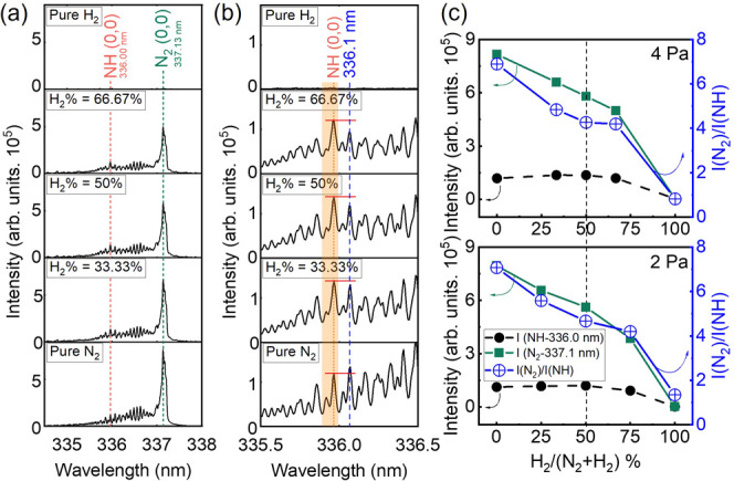
High-resolution optical emission spectra of N2/H2 plasmas at various N2/H2 gas ratios (a) at the wavelength ranging from 334.5 to 338 nm and (b) at the wavelength ranging from 335.5 to 336.5 nm. (c) Relationship between optical emission intensity of N2 and NH of N2/H2 plasmas at various N2/H2 gas ratios and working pressures of 4 and 2 Pa. Excitation power: 300 W, bias power: 200 W, and substrate temperature: 20 °C. The error bars in this figure are smaller than the symbol size.
Figure 5a shows the positions of the NH-336.00 nm peak and N2-337.13 nm peak. The NH peak is overlapped by the tail of the N2 337.13 nm peak, as shown in Figure 5b, so even when using pure N2 plasma, this peak can still be seen. In addition, H atoms and molecules can easily penetrate the chamber wall, so a small amount of hydrogen is still present in the pure N2 plasma. The NH peak becomes clearer with an increase in the H2 %. The intensity of the N2 peak decreases linearly, while the intensity of the NH peak slightly increases as the H2 concentration reaches 50% (Figure 5c). Both the intensities of the N2 peak and the NH peak decrease when continuously increasing the H2 % from 50% to 100%, but the decrease in the N2 intensity is more rapid. The ratios between the intensity of the N2 (337.1 nm) band head and that of NH at 2 Pa are slightly higher than the ratio at 4 Pa. For example, at a H2 % of 50%, these ratios are 4.67 (2 Pa) and 4.26 (4 Pa), as shown in Table 2.
Table 2 presents the relationship between the intensity ratios of I(N2-337.1 nm)/I(Hα-656.3 nm) and I(N2-337.1 nm)/I(NH-336.0 nm) with the etch rate of TiAlC at an H2 % of 50%. N2/H2 plasmas can produce N2, N, H, and NH species. The ratio I(N2-337.1 nm)/I(Hα-656.3 nm) at 2 Pa is 6.18, which is much higher as compared to that at 4 Pa (1.63), and the ratio I(N2-337.1 nm)/I(NH-336.0 nm) at 2 Pa is 4.67, which is slightly higher as compared to that at 4 Pa (4.26). These two ratios show the same tendency with the etch rate of TiAlC. A higher etch rate of TiAlC can be obtained at 2 Pa (3.02 nm/min) than that at 4 Pa (1.85 nm/min). This indicates that the reaction of N2/H2 plasma with TiAlC to form volatile products involves not only NH and H as reactive species but also N species. These nitrogen-containing species play a crucial role in etching TiAlC. In addition to the ratios of reactive species, lower pressure can enhance the volatility of byproducts that were formed by the reaction of N2/H2 plasma with the TiAlC surface.
The optical emission lines of the N atom are at 673.7,44 740, 820, and 860 nm.45 These peaks overlap with the emission band of the N2 molecules, making it difficult to quantify the absolute density of H and N atoms in their ground states. Our research group reported that, using vacuum ultraviolet absorption spectroscopy, an N density of 1.6 × 1011 cm–3 and an H density of 3 × 1011 cm–3 were obtained at the H2 % of 50% with an excitation power of 400 W in the same reactor.46 Based on the previous results, the absolute density of N atoms and H atoms in our study can be estimated to be on the order of 1010 to 1011 cm–3.
3.3. Surface Modification of TiAlC by the N2/H2 Plasmas
The surface modification of the TiAlC film before and after exposure to N2/H2 plasma is shown in Figure 6 (also see Supporting Information, Table S4). As can be seen in Ti 2p and Al 2p spectra, the pristine TiAlC surface before plasma exposure was covered by native oxides Ti–O and Al–O. Active plasma species from N2/H2 plasma such as N, H, and NH react with the TiAlC surface and replace the native oxides Ti–O and Al–O bonds to become Ti–N and Al–N bonds. It is worth noting that although the TiAlC sample after N2/H2 plasma treatment was exposed in the air and then measured by XPS, the N2/H2 plasma-treated TiAlC samples were not reoxidized significantly, meaning that the reaction products containing Ti–N and Al–N bonds can act as a barrier to avoid the oxidation of the air environment. Based on the work of Biesinger et al.47 and Chang and Chiu,48 the Ti 2p spectrum was deconvoluted, as shown in Figure 6a. On the basis of the Shirley background, the Ti 2p peak of the pristine sample could be fitted into three components located at 455.5 eV for Ti 2p3/2 of Ti–C, 456.5 eV for Ti 2p3/2 of O–Ti–C, and 459.4 eV for 2p3/2 of Ti–O. After N2/H2 plasma treatment, the components of Tip 2p3/2 at 456.3 eV for N–Ti–C, 457.3 eV for Ti–N, and 458.3 eV for O–Ti–N obviously appeared.
Figure 6.
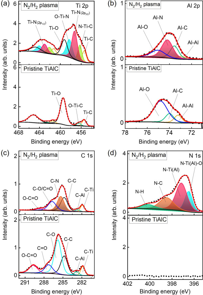
XPS spectra of the TiAlC surface before and after N2/H2 plasma treatment for elements (a) Ti 2p, (b) Al 2p, (c) C 1s, and (d) N 1s. Excitation power: 300 W, bias power: 200 W, N2/H2 ratio: 50/50, working pressure: 2 Pa, and substrate temperature: 20 °C.
Figure 6b shows the bonds Al–Al, Al–C, Al–N, and Al–O, respectively, located at 72.9, 73.6, 74.2, and 75.0 eV. The C 1s peak was deconvoluted with an agreement with Biesinger and Grey49,50, in which the C–Ti bond (281.9 eV), C–Al bond (282.7 eV), C-C bond (284.8 eV), and C–N bond (285.3 eV) were assigned (Figure 6c). The N 1s peak after N2/H2 treatment was deconvoluted as O–Ti(N)–N (396.4 eV), Ti(Al)–N (397.0 eV), C–N (398.4 eV), and N–H (400.0 eV), and, as shown in Figure 6d. In addition to metal-N bonds, N–C and N–H bonds can also be detected. In the study of Vandenbroucke et al., the peaks of tetrakis(dimethylamino)titanium (TDMAT) were detected at 398.0 eV [(H3C)2N–Ti] and 400.4 eV (N–C).51
In comparison with forming metal hydrides, Ti–N and Al–N have similar properties to Ti–C and Al–C in terms of bond length and bond energy. Nitridation of TiAlC is possible, as demonstrated in our previous study.19 Ti–N, Al–N, Ti–C, and Ti–C bonds are not as stable as the Ti–O and Al–O bonds. It is expected that these unstable nitride and carbide bonds after being treated by N2/H2 plasma with numerous dangling bonds can react easily with H atoms to form methylated metal (M-CH3), methylaminated metal (M-N–CH3), amidated metal (M-NH2), or hydrogenated metal (M-H) which are the parts of the volatile products.
3.4. In Situ Monitoring the Modification of the TiAlC Surface Structure during One Cycle Etching Using N2/H2 Plasmas
To investigate the dependence of TiAlC surface modification on bias power after 1 min of N2/H2 plasma exposure, absorbance change of the TiAlC surface at bias powers of 0 W (B0W), 50 W (B50W), 100 W (B100W), and 200 W (B200W) obtained from the in situ ATR-FTIR is presented in Figure 7. The experiment was done with the sequence of 0 to 50 W to 100 W and to 200 W. The reference spectrum for each absorbance spectrum was the preceding one. This means that the reference spectrum for the absorbance spectrum under the conditions without bias (B0W) was the spectrum of pristine TiAlC before applying N2/H2 plasma (treated by Ar sputtering). For the condition using bias power (B50W), the reference spectrum is that of condition B0W. The positive value means mainly surface modification, and the negative value means etching or surface modification and etching simultaneously occurring with the dominant of etching. For the N–H stretch vibration at the absorption band ranging from 3000 to 3500 cm–1, the peak is positive at 0 W and gradually decreases with an increase of bias power to 200 W (Figure 7a). A similar tendency can be observed in the area ranging from 1000 to 1300 cm–1 (Figure 7b). There are many absorption peaks between 800 and 1300 cm–1, namely, spectral feature X. The assignment for the peaks in this region is complicated with many overlapped peaks, which can be discussed later with the simulation results.
Figure 7.
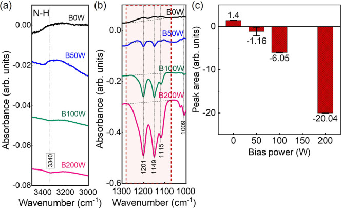
Absorbance change of the TiAlC surface was measured after 1 min of N2/H2 plasma exposure at bias powers of 0 W (B0W), 50 W (B50W), 100 W (B100W), and 200 W (B200W). Data were obtained using in situ ATR-FTIR, focusing on two specific regions: (a) N–H stretch vibration band (3000–3500 cm–1) and (b) spectral feature ranging from 1000 to 1300 cm–1. (c) The absorbance peak area was obtained by integrating the intensities over the wavenumber ranging from 1070 to 1288 cm–1, using a linear baseline. Excitation power: 300 W, N2/H2 ratio: 50/50, working pressure: 2 Pa, and substrate temperature: 20 °C.
As shown in Figure 7c, a significant change of peak area for the absorbance calculated in the wavenumber ranging from 1070 to 1288 cm–1 at bias power 0 W is 1.40, bias power 50 W is −1.16, bias power 100 W is −6.05, and bias power 200 W is −20.04. The dependence of peak area on bias power indicates that without bias power, only surface modification of TiAlC occurs at the excitation power of 300 W. The etching occurs when applying the bias power.
During the continuous etching of TiAlC, surface modification and etching occur simultaneously, so it is difficult to understand the etching mechanism. The separation of surface modification (without using bias power) and etching (with using bias power) is important to understand the plasma–surface reaction, suggesting the concepts for the development of the atomic layer etching (ALE) process. Details of the ALE-like process conditions for N2/H2 plasma exposure and ATR-FTIR results for one cycle of modification/etching of TiAlC at various H2% ratios are described in Table 3.
Table 3. Details of the ALE-like Process Conditions for N2/H2 Plasma Exposure and ATR-FTIR Results for One Cycle of Modification/Etching of TiAlC at Various H2% Ratiosa.
| H2% | process | bias power (W) | exposure time (min) | area (arb. units) | total area change (arb. units) |
|---|---|---|---|---|---|
| 20 | modification | 0 | 4.1 | 8.93 ± 0.05 | |
| etching | 200 | 1 | –13.3 ± 0.60 | 22.23 | |
| 50 | modification | 0 | 3.2 | 8.72 ± 0.12 | |
| etching | 200 | 1 | –12.73 ± 0.54 | 21.45 | |
| 75 | modification | 0 | 3.4 | 8.84 ± 0.16 | |
| etching | 200 | 1 | –12.79 ± 0.57 | 21.63 |
The peak area for the absorbance was integrated over the intensities in the wavenumber ranging from 800.3 to 1388.5 cm–1 with a linear base line. Excitation power: 300 W.
The absorbance changes of the TiAlC during one cycle of plasma–surface reactions (modification-etching) of TiAlC using N2/H2 plasma exposure for surface modification (without using bias power) and etching (using bias power) obtained from in situ ATR-FTIR are demonstrated here, as shown in Figure 8. The reference spectrum for each absorbance spectrum is the preceding one. To reach the self-limitation for surface modification, the plasma exposure time for surface modification was carried out until there was no increase of film thickness (in situ ellipsometry was carried out at the same time) around 3–4 min for surface modification and etching for 1 min for one cycle of each N2/H2 ratio.
Figure 8.
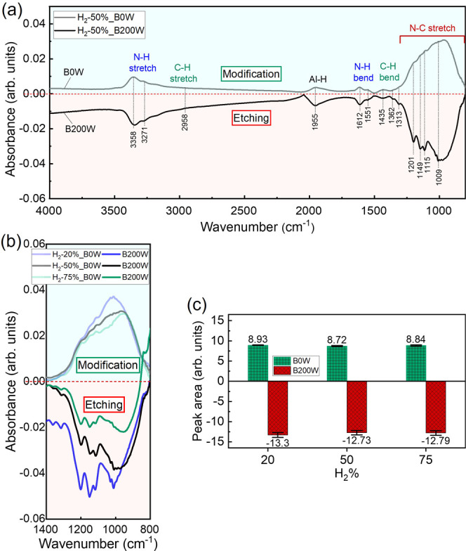
Absorbance change of the TiAlC during one cycle etching using N2/H2 plasma exposure for surface modification (without using bias power, B0W) and etching (using bias power, B200W) obtained from in situ ATR-FTIR for (a) one cycle at the H2 % of 50% and (b) one cycle at various H2 % with the wavenumber ranging from 800 to 1388.5 cm–1. (c) The absorbance peak area was obtained by integrating the intensities over the wavenumber ranging from 800 to 1388.5 cm–1, using a linear baseline. Excitation power: 300 W, bias power: 200 W, N2/H2 ratio: 50/50, working pressure: 2 Pa, and substrate temperature: 20 °C.
Figure 8a shows that ATR-FTIR analysis after the surface of TiAlC was modified by N2/H2 plasma exposure at an H2 % of 50%. The modified TiAlC surface has an absorption band between 3100 and 3450 cm–1 (attributed to the N–H stretching vibration peaks), around 2985 cm–1 (attributed to the C–H stretching vibration peaks), around 1955 cm–1 (attributed to the Al–H vibration peaks), around 1612 cm–1 (attributed to the N–H bending vibration peaks), between 1300 and 1500 cm–1 (attributed to the C–H bending vibration peaks), and between 800 and 1300 cm–1 (possibly attributed to the N–C bending vibration peaks). The modified layer was formed with the positive absorption bands, whereas these bands become negative when etching occurred. The absorbance peak area was calculated for the vibration band ranging from 800.3 to 1388.5 cm–1, as shown in Figure 8b and Table 3. The modified area can be obtained around 8.7–8.9, the etch area can be obtained around 12.7–13.3 for all the H2 ratios from 20% to 75%, and the total area change for all of the conditions is around 21.5–22.2.
To understand experimental spectra and predict volatile products, DFT can be used to suggest IR band assignments due to the fact that the difficulty of interpretation of IR for chemical structures is bonds broken/formed through reaction, loss of symmetry upon precursor adsorption, strong polarization effects, and limitations in measurement at low concentration such as monolayer coverage.25 Volatile candidates can contain bonds such as M-H, M-NH2, M-N(CH2), M-N(CH3)2, M-N(CHNH)2, M-CH3, or M-CN, where M is a metal (Al or Ti in this study). The DFT-calculated IR spectra of potential volatile products of Al-based organometallic molecules and Ti-based organometallic molecules are presented in Figures S3 and S4 (see the Supporting Information). High-intensity N–C stretching vibration peaks can be seen in the simulated IR spectra of Al(N(CH3)2)3 at 976, 1158, and 1273 cm–1 and Ti(N(CH3)2)4 at 936, 1138, and 1239 cm–1. Based on simulated results, the absorption band X between 800 and 1300 cm–1 can be attributed to the vibration peaks of the N–C band. The vibration peaks of C–C/C–O bonds (1080 cm–1),52 –CH=CH2 bond (860 cm–1),53 Ti(Al)–C bond of the pristine TiAlC film, and Ti(Al)–N bond of the modified layer can also coexist in this region.
The potential volatile products (organometallic compounds) formed by the reaction between N2/H2 plasma and the TiAlC surface are presented in Table S5 (see the Supporting Information). These candidates, such as trimethylaluminum, tris(dimethylamido)aluminum(III), and dimer tetrakis(dimethylamido)titanium(IV), contain methylated metal (M-CH3) and methylaminated metal (M-N–CH3) groups and exhibit high volatility or low boiling points (less than 126 °C). Therefore, it is possible that the volatile products formed by the reaction between TiAlC and N2/H2 plasmas have similar structures. In addition to the chemicals having a single bond type between metal and methyl (M-CH3), methylamine (M-N–CH3), or amide (M-NH2), the volatile products can also be combinations of different bonds, such as Al(CH3)(NH2)H and Ti(N(CH3)2)(NH2)3, as shown in Figure 9. This assumption is based on the ATR-FTIR results and simulation results, where the peak positions closely match. To cover a variety of assumptions, the formula M(N(CH3)2)a(CH3)b(NH2)cHd can represent volatile products, where M is a metal (Al or Ti in this study) and a, b, c, d, and e range from 0 to 4.
Figure 9.
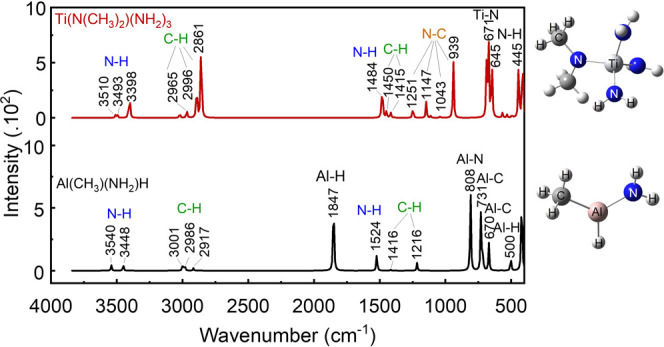
DFT-calculated IR spectra of Ti(Al)-based organometallic molecules Al(CH3)(NH2)H and Ti(N(CH3)2)(NH2)3. The inset images are their molecular structures.
3.5. Surface Roughness of the TiAlC Film after Etching by N2/H2 Plasmas
To evaluate the damage to the surface of TiAlC films etched by N2/H2 plasmas, the surface roughness of TiAlC films before and after N2/H2 plasma etching is presented in Figure 10. The smooth surface of TiAlC films etched by N2/H2 plasma was achieved with an rms of 0.27–0.46 nm, compared to 0.44 nm for the pristine TiAlC film. Figure 10a shows line profiles for surface roughness of TiAlC films etched by N2/H2 plasmas at various H2 % with 3D AFM images (insets). The surface of all the TiAlC films etched by N2/H2 plasma for 5 min is quite uniform with similar properties to that of the pristine surface (rms ≤0.5 nm). For the TiAlC film etched by pure N2 plasma (H2 % = 0%), although no obvious etching occurs (Figure 2), the surface roughness becomes smoother (rms = 0.27 nm) due to the influence of the sputtering effect, as presented in Figure 10b. For the TiAlC films exposed by pure H2 plasma (H2 % = 100%), although no etching occurs, an increase in surface roughness (rms = 0.50 nm) is due to the implantation of H atoms and ions into the TiAlC film. Figure 10c exhibits the dependence of surface roughness (rms) of TiAlC films on plasma exposure time at H2 % of 50%. The surface roughness of the TiAlC film after 5 min of etching is almost the same as that of pristine TiAlC film (rms = 0.44 nm) and slightly reduces to 0.40 nm after 10 min of etching.
Figure 10.
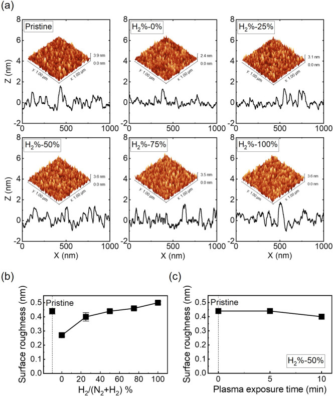
(a) Line profiles for surface roughness of TiAlC films etched by N2/H2 plasmas at various H2 %. Insets show 3D AFM images. (b) Surface roughness (rms) of TiAlC films etched by N2/H2 plasmas at various H2 %. (c) Dependence of surface roughness (rms) of TiAlC films on plasma exposure time at H2 % of 50%. Excitation power: 300 W, bias power: 200 W, working pressure: 2 Pa, and substrate temperature: 20 °C.
Although Ti, Al, and C can be etched by fluorine- or chlorine-based plasmas, the difference in etch rates of Al, Ti, and C can cause rough etched morphologies, which have been discussed in the work of C. Pakpum and N. Pussadee.16 The pre-etch AlTiC surface has a roughness (the arithmetic mean roughness, Ra) of 0.98 ± 0.55 nm, while the surface etched by BCl3/Cl2/Ar plasma has a roughness of 110.7 ± 13.7 nm. The results for the surface roughness of AlTiC etched by CF4 plasma and BCl3/Cl2/Ar plasmas indicate that the etched surface of all halogen-treated AlTiC samples shows significant increases of 2 orders of magnitude in surface roughness (more than 100 nm) compared to that of the pristine sample (around 1 nm). The smooth or low-damage TiAlC surface obtained by N2/H2 plasma etching in our study indicates that there is no obvious selective etching for each element (Ti, Al, and C) by N2/H2 plasma etching. The surface roughness of TiAlC films etched by N2/H2 plasma can be controlled at the atomic level. This is an important result for semiconductor applications.
3.6. Proposed Mechanism of Dry Etching TiAlC by N2/H2 Plasma
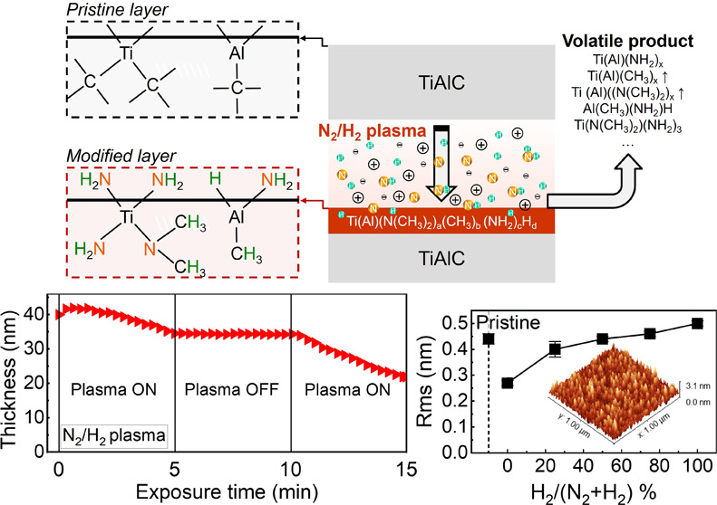
Based on the analysis of the plasma properties, etching rate, surface modifications, and surface roughness of TiAlC films exposed to N2/H2 plasma using OES, in situ spectroscopic ellipsometry, XPS, in situ ATR-FTIR, and AFM, the proposed etching reaction mechanism between N2/H2 plasma and the TiAlC surface is presented in Figure 11. The XPS results (Figure 6) show that the formation of N–H, C–N, and Ti(Al)–N bonds is crucial for the formation of volatile products. Groups such as methylated (−CH3) metal, methylaminated (-N-(CH3)2) metal, aminated (−NH2) metal, and hydrogenated (−H) metal can be part of the candidate products, as shown in the FTIR results (Figure 8), the DFT results (Figures S3 and S4, and Figure 9), and Table S5. By utilization of the synergy effect of N and H in terms of both chemical and physical characteristics during the exposure of the metal carbide surface to N2/H2 plasma, a defective nitride and carbide layer can form, containing with multiple dangling bonds which are capable of trapping numerous hydrogen atoms. H atoms diffused and accumulated in the defective nitride and carbide layer, thereby accelerating the reaction of metal nitride and carbide with H atoms and forming volatile products.
Figure 11.
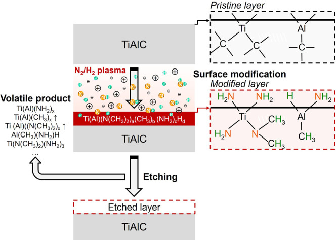
Proposed mechanism for etching TiAlC using N2/H2 plasma.
The Ti oxides and Al oxides are low permeability materials.54,55 These native oxides are very stable because the high dissociation energies of Ti–O and Al–O are 662 and 512 kJ/mol, respectively, compared to those of other Ti and Al compounds, as presented (see Supporting Information, Table S6). The bond length of Al–O is 1.87 Å that is almost 50% shorter in comparison with those of Al–C (3.88 Å) and Al–N (3.83 Å). This Al oxide layer with high density can hinder the reaction of Al–C with other reactive species. Therefore, removing these native oxides is important. The pristine TiAlC film used in this study has a columnar structure that can trap and react with the O atoms during the deposition process, so some amount of Ti–O and Al–O still existed not only on the TiAlC surface (respectively see the XPS result from Figure 6a,b) but also inside the columnar structure (see Supporting Information, Figure S2). Those oxides become passivation parts to avoid the reaction of Al–C and Ti–C with reactive species, resulting in difficulty in etching this material. Ar sputtering is supposed to be able to remove the native oxides from the TiAlC surface; however, it is not able to go deeply to the TiAlC film to remove the Ti–O and Al–O bonds between the columnar regions. Replacing Ti–O and Al–O with bonds of lower dissociation energy can reduce the surface bonding energy of Ti–C and Al–C covered by the native oxides that exist not only on the top surface of the TiAlC film but also within its columnar structure. Although the C–N bond can be formed after N2/H2 plasma exposure, as shown in the C 1s spectrum (Figure 6c), the C–Ti bond still remained, meaning that N atoms do not fully replace C of the metal carbide, but they filled the C vacancy in the polycrystal TiAlC and reacted with Ti–O and Al–O bonds that exist inside the columnar structure of the TiAlC film to form Ti–N and Al–N bonds (Figure 6). The H atom has a small radius (1.54 Å), so it can penetrate deeply to the TiAlC film and potentially replaces the O atom in metal oxides to become metal hydrides with much lower bond energies such as Al–H (285 kJ/mol) and Ti–H bond (1.70 kJ/mol). However, H penetration to the metal film may produce an active vacancy–hydrogen complex in the metal part, and these nonequilibrium vacancies tend to segregate, forming void in the metal bulk.56−58 Moreover, in the consideration of etching aspect, due to the low volatility of TiHx and AlHx, as mentioned in the study of Choi and Hess,29 pure H2 plasma is not a good candidate to etch TiAlC. In comparison with forming metal hydrides, Ti–N and Al–N have similar properties with Ti–C and Al–C in terms of bond length and bond energy and are not stable as Ti–O and Al–O bonds. The defective nitride and carbide layer, formed after exposure to N2/H2 plasma, contains multiple dangling bonds that are capable of trapping numerous hydrogen atoms. A similar effect was studied when using plasma to grow a nitride layer, which can act as a hydrogen trapping layer for austenitic stainless steel film.59 Therefore, these unstable nitrides and original carbide bonds after treatment by N2/H2 plasma can have numerous dangling bonds to react easily with H atoms to form methylated metal (M-CH3), methylaminated metal (M-N–CH3), amidated metal (M-NH2), or hydrogenated metal (M-H) bonds that are parts of the volatile products, as shown in the FTIR results (Figure 8), the DFT results (Figures S3 and S4, and Figure 9), and Table S5. For more considerations about the volatile products, the methyl group (CH3−) can be another alkyl group (CnH2n+1−). In addition to the forming volatile metal hydrides, methylated metal or alkylated metal etch products generated with hydrocarbon etching plasma were investigated.60,61 Therefore, in this study, by controlling the active species such as N, NH, and H, methylation, methylamination, amination, and hydrogenation of the TiAlC film can be formed and become part of the volatile products. Importantly, the surface roughness of the TiAlC film etched by N2/H2 plasma in this study can be controlled at the atomic level (rms around 0.4 nm). This indicates that there is no obvious selective etching for each element (Ti, Al, and C) by N2/H2 plasma etching, providing useful insights into the microfabrication for large-scale integrated circuits in semiconductor devices.
4. Conclusions
A simple, highly controllable, and dry etching method for ternary metal carbides TiAlC using nonhalogen N2/H2 plasmas at low pressure and 20 °C is presented. The etch rate of TiAlC was around 3 nm/min using the N2/H2 plasma at an excitation power of 300 W, a bias power of 200 W, and 2 Pa. Almost no etching occurred when using pure N2 plasma or pure H2 plasma. The NH molecular line at 336 nm from N2/H2 plasmas was detected using HR-OES. The relationship between the intensity ratios of I(N2-337.1 nm)/I(Hα-656.3 nm) and I(N2-337.1 nm)/I(NH-336.0 nm) and the etch rate of TiAlC, with higher intensity ratios resulting in a higher etch rate at lower pressure (2 Pa), was investigated. The formation of N–H and C–N bonds on TiAlC during the plasma–surface reaction between N2/H2 plasma and TiAlC was detected using XPS and in situ ATR-FTIR, indicating that the N2/H2 plasmas contain etchant species including N, NH, and H that react with the metal carbide surface to form methylated (−CH3)–, methylaminated (−N–(CH3)2)–, aminated (−NH2)–, and hydrogenated (−H) metals as volatile products. After N2/H2 etching, a smooth etched surface was achieved with an rms of 0.40 nm, comparable to the initial roughness of 0.44 nm. The results demonstrate a concept for developing etching of metal carbide using low-pressure and low-temperature nonhalogen plasmas through transformation reactions between inorganic materials (metal carbide) and inorganic etchants (N2/H2 plasma) to form volatile organic compounds using nonhalogen, noncorrosive, nontoxic gases, or nonorganic compound etchants.
Acknowledgments
The authors would like to thank Prof. Nikolay Britun at Center for Low-temperature Plasma Sciences (cLPS), Nagoya University for his support of using the high-resolution optical emission spectroscopy measurement, Liugang Hu for the discussion about using the Gaussian program, and Shohei Nakamura for supporting AFM measurement.
Data Availability Statement
The data sets generated during and/or analyzed during the current study are available from the corresponding author on reasonable request.
Supporting Information Available
The Supporting Information is available free of charge at https://pubs.acs.org/doi/10.1021/acsami.4c11025.
Best fit parameters of the TiAlC layer obtained by the Gen-Osc model, XRD pattern of pristine TiAlC film grown on Si wafer, in situ XPS spectra and atomic percentage of TiAlC before and after Ar sputter, atomic radii and atomic weights of the elements used in this study, film thickness change of TiAlC before and after exposing to N2/H2 plasmas, details of peak binding energy and full width at half-maximum of TiAlC film before and after exposure to N2/H2 plasma, DFT-calculated IR spectra of Al-based organometallic molecules, DFT-calculated IR spectra of Ti-based organometallic molecules, boiling points of potential volatile products, and bond length and bond dissociation energy of metal–metal (M–M) and metal compounds (M–X) (PDF)
Author Contributions
Thi-Thuy-Nga Nguyen: conceptualization, data curation, formal analysis, investigation, methodology, visualization, and writing—original draft. Kazunori Shinoda: resources, data curation, and validation. Shih-Nan Hsiao: resources, data curation, and validation. Kenji Maeda: resources and validation. Kenetsu Yokogawa: funding acquisition and validation. Masaru Izawa: project administration and supervision. Kenji Ishikawa: funding acquisition and validation. Masaru Hori: project administration, validation, and supervision. All authors have discussed and agreed to the published version of the manuscript.
The authors declare no competing financial interest.
Supplementary Material
References
- Xiang J.; Li T.; Zhang Y.; Wang X.; Gao J.; Cui H.; Yin H.; Li J.; Wang W.; Ding Y.; Xu C.; Zhao C. Investigation of TiAlC by Atomic Layer Deposition as N Type Work Function Metal for FinFET. ECS J. Solid State Sci. Technol. 2015, 4 (12), P441–P444. 10.1149/2.0231512jss. [DOI] [Google Scholar]
- Westlinder J.; Sjöblom G.; Olsson J. Variable Work Function in MOS Capacitors Utilizing Nitrogen-Controlled TiNx Gate Electrodes. Microelectron. Eng. 2004, 75 (4), 389–396. 10.1016/j.mee.2004.07.061. [DOI] [Google Scholar]
- Lima L. P. B.; Dekkers H. F. W.; Lisoni J. G.; Diniz J. A.; Elshocht S. V.; Gendt S. D. Metal gate work function tuning by Al incorporation in TiN. J. Appl. Phys. 2014, 115 (7), 074504. 10.1063/1.4866323. [DOI] [Google Scholar]
- Jeon S.; Park S. Tunable Work-Function Engineering of TiC–TiN Compound by Atomic Layer Deposition for Metal Gate Applications. J. Electrochem. Soc. 2010, 157 (10), H930. 10.1149/1.3459932. [DOI] [Google Scholar]
- Jyothi J.; Biswas A.; Sarkar P.; Soum-Glaude A.; Nagaraja H. S.; Barshilia H. C. Optical Properties of TiAlC/TiAlCN/TiAlSiCN/TiAlSiCO/TiAlSiO Tandem Absorber Coatings by Phase-Modulated Spectroscopic Ellipsometry. Appl. Phys. A: Mater. Sci. Process. 2017, 123 (7), 496. 10.1007/s00339-017-1103-2. [DOI] [Google Scholar]
- Oniki Y.; Altamirano-Sánchez E.; Holsteyns F. (Invited) Selective Etches for Gate-All-Around (GAA) Device Integration: Opportunities and Challenges. ECS Trans. 2019, 92 (2), 3–12. 10.1149/09202.0003ecst. [DOI] [Google Scholar]
- Cui S.; Sun K.; Liao Z.; Zhou Q.; Jin L.; Jin C.; Hu J.; Wen K. S.; Liu S.; Zhou S. Flexible Nanoimprint Lithography Enables High-Throughput Manufacturing of Bioinspired Microstructures on Warped Substrates for Efficient III-Nitride Optoelectronic Devices. Sci. Bull. 2024, 69 (13), 2080–2088. 10.1016/j.scib.2024.04.030. [DOI] [PubMed] [Google Scholar]
- Zhou S.; Liu X.; Yan H.; Chen Z.; Liu Y.; Liu S. Highly Efficient GaN-Based High-Power Flip-Chip Light-Emitting Diodes. Opt. Express 2019, 27 (12), A669. 10.1364/OE.27.00A669. [DOI] [PubMed] [Google Scholar]
- Zhou S.; Zhao X.; Du P.; Zhang Z.; Liu X.; Liu S.; Guo L. J. Application of Patterned Sapphire Substrate for III-Nitride Light-Emitting Diodes. Nanoscale 2022, 14, 4887–4907. 10.1039/d1nr08221c. [DOI] [PubMed] [Google Scholar]
- Altieri N. D.; Chen J. K.-C.; Minardi L.; Chang J. P. Review Article: Plasma–Surface Interactions at the Atomic Scale for Patterning Metals. J. Vac. Sci. Technol., A 2017, 35 (5), 050203. 10.1116/1.4993602. [DOI] [Google Scholar]
- Johnson N. R.; Sun H.; Sharma K.; George S. M. Thermal Atomic Layer Etching of Crystalline Aluminum Nitride Using Sequential, Self-Limiting Hydrogen Fluoride and Sn(Acac)2 Reactions and Enhancement by H2 and Ar Plasmas. J. Vac. Sci. Technol., A 2016, 34 (5), 050603. 10.1116/1.4959779. [DOI] [Google Scholar]
- Cano A. M.; Lii-Rosales A.; George S. M. Thermal Atomic Layer Etching of Aluminum Nitride Using HF or XeF2for Fluorination and BCl3for Ligand Exchange. J. Phys. Chem. C 2022, 126 (16), 6990–6999. 10.1021/acs.jpcc.1c10972. [DOI] [Google Scholar]
- Hsiao R.; Miller D.; Nguyen S.; Kellock A. Titanium Carbide Etching in High Density Plasma. Appl. Surf. Sci. 1999, 148, 1–8. 10.1016/S0169-4332(99)00143-9. [DOI] [Google Scholar]
- Pakpum C.; Limsuwan P. A Deep AlTiC Dry Etching for Fabrication of Burnish and Glide Slider Head. Procedia Eng. 2012, 32, 1037–1042. 10.1016/j.proeng.2012.02.051. [DOI] [Google Scholar]
- Fukushima N.; Katai H.; Wada T.; Horiike Y. High-Rate and Smooth Surface Etching of Al2O3-TiC Employing Inductively Coupled Plasma (ICP). Jpn. J. Appl. Phys. 1996, 35, 2512. 10.1143/jjap.35.2512. [DOI] [Google Scholar]
- Pakpum C.; Pussadee N. Deep Reactive Ion Etching of Alumina Titanium Carbide Using Chlorine-Based Plasma. Surf. Coat. Technol. 2016, 306, 194–199. 10.1016/j.surfcoat.2016.05.076. [DOI] [Google Scholar]
- DuMont J. W.; George S. M. Competition between Al2O3 Atomic Layer Etching and AlF3 Atomic Layer Deposition Using Sequential Exposures of Trimethylaluminum and Hydrogen Fluoride. J. Chem. Phys. 2017, 146 (5), 052819. 10.1063/1.4973310. [DOI] [PubMed] [Google Scholar]
- Clancey J. W.; Cavanagh A. S.; Smith J. E. T.; Sharma S.; George S. M. Volatile Etch Species Produced during Thermal Al2O3 Atomic Layer Etching. J. Phys. Chem. C 2020, 124 (1), 287–299. 10.1021/acs.jpcc.9b06104. [DOI] [Google Scholar]
- Nguyen T. T. N.; Shinoda K.; Hamamura H.; Maeda K.; Yokogawa K.; Izawa M.; Ishikawa K.; Hori M. Dry Etching of Ternary Metal Carbide TiAlC via Surface Modification Using Floating Wire-Assisted Vapor Plasma. Sci. Rep. 2022, 12 (1), 20394. 10.1038/s41598-022-24949-1. [DOI] [PMC free article] [PubMed] [Google Scholar]
- Nguyen T. T. N.; Sasaki M.; Odaka H.; Tsutsumi T.; Ishikawa K.; Hori M. Remotely Floating Wire-Assisted Generation of High-Density Atmospheric Pressure Plasma and SF6 -Added Plasma Etching of Quartz Glass. J. Appl. Phys. 2019, 125 (6), 063304. 10.1063/1.5081875. [DOI] [Google Scholar]
- Nguyen T. T. N.; Sasaki M.; Tsutsumi T.; Ishikawa K.; Hori M. Formation of Spherical Sn Particles by Reducing SnO2 Film in Floating Wire-Assisted H2/Ar Plasma at Atmospheric Pressure. Sci. Rep. 2020, 10 (1), 17770. 10.1038/s41598-020-74663-z. [DOI] [PMC free article] [PubMed] [Google Scholar]
- Nguyen T. T. N.; Sasaki M.; Hsiao S. N.; Tsutsumi T.; Ishikawa K.; Hori M. Low-Temperature Reduction of SnO2 by Floating Wire-Assisted Medium-Pressure H2/Ar Plasma. Plasma Processes Polym. 2022, 19 (6), 2100209. 10.1002/ppap.202100209. [DOI] [Google Scholar]
- Frisch M. J.; Trucks G. W.; Schlegel H. B.; Scuseria G. E.; Robb M. A.; Cheeseman J. R.; Scalmani G.; Barone V.; Petersson G. A.; Nakatsuji H.. Gaussian 16. Revision C.01; Inc.: Wallingford CT, 2016.
- Pearse R. W. B.; Gaydon A. G.. The Identification of Molecular Spectra; Chapman & Hall Ltd: London, 1950. [Google Scholar]
- Mustard T. J. L.; Kwak H. S.; Goldberg A.; Gavartin J.; Morisato T.; Yoshidome D.; Halls M. D. Quantum Mechanical Simulation for the Analysis, Optimization and Accelerated Development of Precursors and Processes for Atomic Layer Deposition (ALD). J. Korean Ceram. Soc. 2016, 53 (3), 317–324. 10.4191/kcers.2016.53.3.317. [DOI] [Google Scholar]
- National Institute of Standards and Technology , May 2022. https://cccbdb.nist.gov/vibscalejust.asp.
- Rahm M.; Hoffmann R.; Ashcroft N. W. Atomic and Ionic Radii of Elements 1–96. Chem.—Eur. J. 2016, 22 (41), 14625–14632. 10.1002/chem.201602949. [DOI] [PubMed] [Google Scholar]
- Meija J.; Coplen T. B.; Berglund M.; Brand W. A.; De Bièvre P.; Gröning M.; Holden N. E.; Irrgeher J.; Loss R. D.; Walczyk T.; Prohaska T. Atomic Weights of the Elements 2013 (IUPAC Technical Report). Pure Appl. Chem. 2016, 1, 265–291. 10.1515/pac-2015-0305. [DOI] [Google Scholar]
- Choi T. S.; Hess D. W. Chemical Etching and Patterning of Copper, Silver, and Gold Films at Low Temperatures. ECS J. Solid State Sci. Technol. 2015, 4 (1), N3084–N3093. 10.1149/2.0111501jss. [DOI] [Google Scholar]
- Choi T.-S.; Levitin G.; Hess D. W. Mechanistic Considerations in Plasma-Assisted Etching of Ag and Au Thin Films. ECS J. Solid State Sci. Technol. 2013, 2 (6), P275–P281. 10.1149/2.012306jss. [DOI] [Google Scholar]
- Wu F.; Levitin G.; Hess D. W. Low-Temperature Etching of Cu by Hydrogen-Based Plasmas. ACS Appl. Mater. Interfaces 2010, 2 (8), 2175–2179. 10.1021/am1003206. [DOI] [Google Scholar]
- Wu F.; Levitin G.; Choi T. S.; Hess D. W. Subtractive Etching of Cu at Low Temperature in Hydrogen-Based Plasmas. ECS Trans. 2012, 44 (1), 299. 10.1149/1.3694330. [DOI] [Google Scholar]
- Trieschmann J.; Ries S.; Bibinov N.; Awakowicz P.; Mráz S.; Schneider J. M.; Mussenbrock T. Combined Experimental and Theoretical Description of Direct Current Magnetron Sputtering of Al by Ar and Ar/N2 Plasma. Plasma Sources Sci. Technol. 2018, 27 (5), 054003. 10.1088/1361-6595/aac23e. [DOI] [Google Scholar]
- Yi C. X.; Wang S. K.; Xu X. B.; Tian Y. F.; Bao M. D. Study on Plasma Cleaning of Surface Contaminants on Pure Copper. Mater. Res. Express 2023, 10, 016506. 10.1088/2053-1591/acac61. [DOI] [Google Scholar]
- Ventura L. R.; Fellows C. E. The N2 second positive (C3Π → B3Π) system reviewed: Improved data and analysis. Quant. Spectrosc. Radiat. Transfer 2019, 239, 106645. 10.1016/j.jqsrt.2019.106645. [DOI] [Google Scholar]
- Jans E. R. Rovibronic Molecular Line List for the N2(C3Πu–B3Πg) Second Positive System. Quant. Spectrosc. Radiat. Transfer 2024, 312, 108809. 10.1016/j.jqsrt.2023.108809. [DOI] [Google Scholar]
- Song M. A.; Lee Y. W.; Chung T. H. Characterization of an Inductively Coupled Nitrogen-Argon Plasma by Langmuir Probe Combined with Optical Emission Spectroscopy. Phys. Plasmas 2011, 18 (2), 023504. 10.1063/1.3554706. [DOI] [Google Scholar]
- Hsu C.-C.; Yang Y.-J. The Increase of the Jet Size of an Atmospheric-Pressure Plasma Jet by Ambient Air Control. IEEE Trans. Plasma Sci. 2009, 38, 496–499. 10.1109/TPS.2009.2038701. [DOI] [Google Scholar]
- Draškovič-Bračun A.; Mozetič M.; Zaplotnik R. E- and H-Mode Transition in a Low Pressure Inductively Coupled Ammonia Plasma. Plasma Processes Polym. 2018, 15 (1), 1700105. 10.1002/ppap.201700105. [DOI] [Google Scholar]
- Gorjanc M.; Mozetič M.; Primc G.; Vesel A.; Spasić K.; Puač N.; Petrović Z. L.; Kert M. Plasma Treated Polyethylene Terephthalate for Increased Embedment of UV-Responsive Microcapsules. Appl. Surf. Sci. 2017, 419, 224–234. 10.1016/j.apsusc.2017.04.177. [DOI] [Google Scholar]
- Tamaki M.; Tomii Y.; Yamamoto N. The Role of Hydrogen in Plasma Nitriding: Hydrogen Behavior in the Titanium Nitride Layer. Plasmas Ions 2000, 3 (1–4), 33–39. 10.1016/S1288-3255(00)00108-8. [DOI] [Google Scholar]
- Ohmi H.; Sato J.; Shirasu Y.; Hirano T.; Kakiuchi H.; Yasutake K. Significant Improvement of Copper Dry Etching Property of a High-Pressure Hydrogen-Based Plasma by Nitrogen Gas Addition. ACS Omega 2019, 4 (2), 4360–4366. 10.1021/acsomega.8b03163. [DOI] [PMC free article] [PubMed] [Google Scholar]
- Fridman A.. In Plasma Chemistry; Fridman A., Ed.; Cambridge University Press: New York, 2008. [Google Scholar]
- Nagai H.; Takashima S.; Hiramatsu M.; Hori M.; Goto T. Behavior of Atomic Radicals and Their Effects on Organic Low Dielectric Constant Film Etching in High Density N2/H2 and N2/NH3 Plasmas. J. Appl. Phys. 2002, 91 (5), 2615–2621. 10.1063/1.1435825. [DOI] [Google Scholar]
- Kuo S. Y.; Kei C. C.; Hsiao C. N.; Chao C. K.; Lai F. I.; Kuo H. C.; Hsieh W. F.; Wang S. C. Catalyst-Free GaN Nanorods Grown by Metalorganic Molecular Beam Epitaxy. IEEE Trans. Nanotechnol. 2006, 5, 273–276. 10.1109/TNANO.2006.874055. [DOI] [Google Scholar]
- Yamamoto H.; Kuroda H.; Ito M.; Ohta T.; Takeda K.; Ishikawa K.; Kondo H.; Sekine M.; Hori M. Feature Profiles on Plasma Etch of Organic Films by a Temporal Control of Radical Densities and Real-Time Monitoring of Substrate Temperature. Jpn. J. Appl. Phys. 2012, 51 (1R), 016202. 10.1143/JJAP.51.016202. [DOI] [Google Scholar]
- Biesinger M. C.; Lau L. W. M.; Gerson A. R.; Smart R. S. C. Resolving Surface Chemical States in XPS Analysis of First Row Transition Metals, Oxides and Hydroxides: Sc, Ti, V, Cu and Zn. Appl. Surf. Sci. 2010, 257 (3), 887–898. 10.1016/j.apsusc.2010.07.086. [DOI] [Google Scholar]
- Chang Y.-H.; Chiu H.-T. Nano-Sizing Titanium into Titanium Carbide by 1-Chlorobutane. J. Mater. Res. 2002, 17 (11), 2779–2782. 10.1557/JMR.2002.0403. [DOI] [Google Scholar]
- Biesinger M. C. Accessing the Robustness of Adventitious Carbon for Charge Referencing (Correction) Purposes in XPS Analysis: Insights from a Multi-User Facility Data Review. Appl. Surf. Sci. 2022, 597, 153681. 10.1016/j.apsusc.2022.153681. [DOI] [Google Scholar]
- Grey L. H.; Nie H. Y.; Biesinger M. C. Defining the Nature of Adventitious Carbon and Improving Its Merit as a Charge Correction Reference for XPS. Appl. Surf. Sci. 2024, 653, 159319. 10.1016/j.apsusc.2024.159319. [DOI] [Google Scholar]
- Vandenbroucke S. S. T.; Levrau E.; Minjauw M. M.; Van Daele M.; Solano E.; Vos R.; Dendooven J.; Detavernier C. Study of the Surface Species during Thermal and Plasma-Enhanced Atomic Layer Deposition of Titanium Oxide Films Using in Situ IR-Spectroscopy and in Vacuo X-Ray Photoelectron Spectroscopy. Phys. Chem. Chem. Phys. 2020, 22 (17), 9262–9271. 10.1039/D0CP00395F. [DOI] [PubMed] [Google Scholar]
- Absalan Y.; Gholizadeh M.; Razavi M. R.; Dastani Z.; Vu A. T. N.; Kovalchukova O. Synthesis of TiC@C-Anatase/Rutile@polyvinyl Alcohol/Xylan: A Powerful Photocatalyst for Degradation of Organic Pollutant under Visible Light. R Soc. Open Sci. 2022, 9 (8), 220080. 10.1098/rsos.220080. [DOI] [PMC free article] [PubMed] [Google Scholar]
- Xiang J.; Ding Y.; Du L.; Li J.; Wang W.; Zhao C. Growth Mechanism of Atomic-Layer-Deposited TiAlC Metal Gate Based on TiCl4 and TMA Precursors. Chin. Phys. B 2016, 25 (3), 037308. 10.1088/1674-1056/25/3/037308. [DOI] [Google Scholar]
- Zhang G.; Dou S.; Lu Y.; Shi Y.; Lai X.; Wang X. Mechanisms for Adsorption, Dissociation and Diffusion of Hydrogen in Hydrogen Permeation Barrier of α-Al2O3: The Role of Crystal Orientation. Int. J. Hydrogen Energy 2014, 39 (1), 610–619. 10.1016/j.ijhydene.2013.10.063. [DOI] [Google Scholar]
- Zeng Y.; Noël J. J.; Norton P. R.; Shoesmith D. W. Hydrogen Transport through Thin Titanium Oxides. J. Electroanal. Chem. 2010, 649 (1–2), 277–285. 10.1016/j.jelechem.2010.06.022. [DOI] [Google Scholar]
- Ganchenkova M. G.; Yagodzinskyy Y. N.; Borodin V. A.; Hänninen H. Effects of Hydrogen and Impurities on Void Nucleation in Copper: Simulation Point of View. Philos. Mag. 2014, 94 (31), 3522–3548. 10.1080/14786435.2014.962642. [DOI] [Google Scholar]
- Turnbull A. Perspectives on hydrogen uptake, diffusion and trapping. Int. J. Hydrogen Energy 2015, 40, 16961–16970. 10.1016/j.ijhydene.2015.06.147. [DOI] [Google Scholar]
- Fukai Y. Superabundant Vacancies Formed in Metal-Hydrogen Alloys. Phys. Scr. 2003, 2003, 11. 10.1238/physica.topical.103a00011. [DOI] [Google Scholar]
- Zakroczymski T.; Flis J.; Lukomski N.; Mankowski J. Entry, Transport and Absorption of Hydrogen in Low-Temperature Plasma Nitrided Austenitic Stainless Steel. Acta Mater. 2001, 49, 1929–1938. 10.1016/s1359-6454(01)00112-4. [DOI] [Google Scholar]
- Choi T.-S.; Hess D. W. Etching of Ag and Au Films in CH4-Based Plasmas at Low Temperature. J. Vac. Sci. Technol., B: Nanotechnol. Microelectron.: Mater., Process., Meas., Phenom. 2015, 33 (1), 012202. 10.1116/1.4902332. [DOI] [Google Scholar]
- Choi T.-S.; Levitin G.; Hess D. W. Low Temperature Cu Etching Using CH4-Based Plasmas. ECS J. Solid State Sci. Technol. 2013, 2 (11), P506–P514. 10.1149/2.002312jss. [DOI] [Google Scholar]
Associated Data
This section collects any data citations, data availability statements, or supplementary materials included in this article.
Supplementary Materials
Data Availability Statement
The data sets generated during and/or analyzed during the current study are available from the corresponding author on reasonable request.


