

Abstract
A DC-DC buck converter (DDBC) plays a crucial role in facilitating the rapid evolution of Internet of Things (IoT) applications across a broad spectrum of load requirements. Achieving high efficiency under diverse load conditions necessitates a meticulous exploration of modulation and control methods. This paper aims to explore literature concerning modulation and control techniques employed in buck converters for IoT applications, with the goal of achieving optimal efficiency. The most often used control methods in the DDBC for power conversion efficiently are adaptive controlled pulse skip modulation (APSM), pulse frequency modulation (PFM), digital pulse width modulation (DPWM), and adaptive on time control (AOT). Based on the major drawbacks of high quiescent current, large ripple, and low efficiency, the control methods used in IoT applications to achieve high efficiency are discussed. The structure of DDBC with the unique controlling method and their capability of suppressing the output ripple voltage and minimizing quiescent current are briefly addressed. Comparison among the methods exhibits how control methods can achieve high efficiency. This paper outlines the major challenges in power converter control for future research and development.
Keywords: High efficiency, Internet of things (IoT), Low ripple, Quiescent current, Synchronous DC-DC buck converter
1. Introduction
The IoT is a contemporary technological advancement enabling the digital transformation of the physical realm through the integration of numerous electrical devices. Forecasts indicate that the future will witness a connection of over 20 billion IoT devices to the internet [1]. These devices actively gather data pertaining to their physical attributes and functionalities, subsequently transmitting this information to the network. Some outputs can control other systems and equipment on their own or using network commands. Miniaturization and autonomous sensor systems required for low-volume battery-powered applications like wearables, medical healthcare, smart home automation and a long-life battery are essential for these requirements [[2], [3], [4]]. To prolong battery lifetime, power management unit into IoT devices is significant in battery-driven IoT applications [5,6].
The standard IoT application comprises a power management section (PMS), sensors, communication systems, and microprocessor units, as illustrated in Fig. 1 Within the realm of IoT systems, the lithium-ion battery emerges as a reliable power source, boasting a voltage range of 2.5 V–4.2 V [7]. IoT devices function in two modes: idle mode, characterized by power consumption ranging from microamperes (μA) to milliamperes (mA) and active mode, where power consumption ranges from mA to several hundred mA. Consequently, inductor-based DC-DC converters (DDC) find greater prevalence in these IoT applications compared to switch-capacitor-based counterparts, owing to the extensive load current range across the operation modes: idle mode and active mode [8,9]. As the pivotal component of the PMS, the converter is required to maintain minimal power consumption and optimal efficiency in both operational modes. Significantly, a substantial portion of the operational time for an IoT system is devoted to idle mode, where the quiescent current of the DDC plays a pivotal role in determining overall power consumption. The implementation of an ultra-low power DDC, characterized by an idle current in the range of hundreds of nanoamperes (nA) becomes crucial for minimizing the energy consumption of IoT devices and extending their battery life [5]. It is imperative that the converter exhibits a swift and seamless response to load transitions, accommodating load current changes from μA to mA. Additionally, for enhanced cost-effectiveness and compactness, the DDC should integrate a microchip and reduced-size external elements including inductors and capacitors aligning with the preferences for low-powered IoT products [[10], [11], [12]].
Fig. 1.

Diagrammatic representation of a standard IoT application.
In the field of IoT devices, maintaining a heightened level of power conversion efficiency poses a significant challenge for DDBC, particularly when operating at ultralight load currents, such as in the microampere (μA) range [4]. To ensure optimal efficiency across diverse load conditions, the implementation of distinct control modes becomes imperative for the buck converter. These modes include PWM, PSM and PFM, each of which must be seamlessly adjusted based on the prevailing load conditions [[13], [14], [15], [16], [17], [18], [19]].Furthermore, achieving ultra-quiescent current and enhancing efficiency at light loads necessitates the integration of an additional controller [16,20,21].
In low-power converters, the incorporation of hybrid control modes becomes imperative for extending the dynamic range. Traditional control approaches encounter low efficiency at ultra-light load conditions, primarily attributable to high quiescent current. A remedy for this challenge is found in the PSM method. PSM efficiently decreases the conduction time of the power MOS transistor by operating at a consistent frequency [22]. This reduction is achieved by strategically” skipping” pulses to mitigate power consumption in gate drivers and switches [23]. The precise configuration of charge and skip cycles for both frequency and count is facilitated through the application of a voltage-mode digital pulse skipping modulator (VDPSM). Efficiency optimization is accomplished by thoughtfully choosing the number of skip cycles [24]. Additionally, activating the PSM mode when the inductor current hits zero effectively suppresses the reverse current, thereby enhancing conversion efficiency [25].
In the context of implantable System-on-Chips (SoCs) [26], a PSM step-up/down converter is employed to minimize quiescent current, achieving an impressive reduction. Addressing the power efficiency challenges in mobile devices, a novel 2.5 MHz integrated dual-phase DDBC is introduced, featuring low quiescent power consumption. To further optimize power utilization under light load conditions, an additional PSM controller is integrated into the design [27]. A unique strategy is employed in proposing a PSM buck converter, featuring a manually adjustable switching frequency and on-time period [28]. This innovative configuration facilitates a dynamic range spanning from 500 pA to 1 mA, showcasing the adaptability and efficiency of the proposed converter design.
The PFM control method is extensively utilized in DDBC operating in discontinuous-conduction mode (DCM), especially in scenarios characterized by light load applications. This preference is attributed to its characteristic slower switching frequency, leading to reduced switching losses in response to varying loads [[29], [30], [31], [32], [33], [34], [35], [36], [37], [38], [39], [40], [41]]. Frequency compensation is not necessary for a PFM buck converter (BC), and it also improves the current accuracy under different load conditions [42,43]. It has significant benefits such as less circuit complexity and reduced fabrication costs for IoT applications. While a PFM BC offers numerous advantages, it is not exempt from a significant drawback which is a large output voltage ripple. A fundamental trade-off emerges between the ripple voltage and the low load efficiency within a PFM BC. While earlier research has effectively tackled the mitigation of controller power loss, a critical aspect frequently disregarded in these investigations is the concurrent minimization of both controller power loss and output voltage ripple [6,17,19].
In response to dynamic load conditions, the reliability of the DDBC may undergo deterioration, resulting in a decline in power efficiency. Therefore, it becomes imperative to adjust the modulation mode in alignment with load variations. The articles [[17], [19], [44], [45], [46]] introduce a unified triple mode (PWM, PFM, and retention mode) integrated into a single chip to optimize power efficiency based on load conditions. The power efficiency of the DDBC is influenced by switching loss, conduction loss and internal control circuit loss [47]. Notably, the PWM mode exhibits superior output regulation characteristics at higher frequencies compared to alternative modes [48]. Conversely, in the PFM mode, performance is compromised due to variable switching frequencies [29]. Remarkably, the retention mode is activated when the load current falls below 500 μA. To mitigate electrical power consumption within internal circuits, both PFM and retention mode controllers are disengaged when PWM mode is activated [19]. These advancements contribute significantly to enhancing the overall operational efficiency of the DDBC, effectively addressing challenges posed by fluctuating load conditions.
The integration of multiple controllers has been explored as a strategy to attain high efficiency across an extensive load spectrum [14,16,18,20,49,50]. However, this approach necessitates the construction of all circuit blocks associated with the various controllers, introducing complexity to the design process. Furthermore, achieving seamless mode transitions poses challenges due to the time delay inherent in making mode change decisions. During the transition between modes, this delay elevates the probability of encountering challenges and random noise. The DDC employed in IoT applications must possess the capability to effectively manage a broad spectrum of load currents ranging from nanoamperes to milliamperes, ensuring a rapid load transient response from nanoamperes/microamperes to milliamperes during transitions between operational modes. IoT devices are categorized into three distinct operation modes based on their load current profiles: inactive mode, idle mode and active mode [18]. Predominantly, IoT devices operate in inactive mode, where the current consumption spans from nanoamperes to tens of microamperes. In idle mode, PFM control is established, resulting in a current consumption of approximately a hundred microamperes. Conversely, in active mode, PWM control is commonly utilized, leading to a current consumption of less than a hundred microamperes [51]. The integration of dual-mode control has been proposed to enhance efficiency across diverse load conditions [[52], [53], [54]].
The demand for resilient power scaling strategies in the context of IoT on System-on-Chips (SoCs) is expected to persist, especially as these devices are increasingly powered by energy harvesters with diminishing dimensions. Various power management approaches, including dynamically adjusting voltage and frequency (DAVF)[[55], [56], [57], [58]] and multimodal control [[59], [60], [61]], have been deployed to optimize the power consumption and performance of SoCs. Employing the DAVF technique requires dynamic adjustments to the SoC's supply voltage and clock frequency based on workload demands and energy availability, ensuring energy savings while adhering to performance standards.
In low-to-medium power DDBC, digital controllers offer numerous advantages, such as reduced sensitivity to process variation, programmability, decreased reliance on passive components for tuning, simplicity, and cost-effectiveness [46,62,63]. Additionally, adopting a digital approach facilitates the straightforward implementation of advanced control algorithms, ensuring optimal transient performance [64]. In traditional digital PWM-based DDBC [[65], [66], [67]], the output voltage ripple is contingent upon the precision of DPWM. Enhancing the ripple characteristics of the output voltage requires an increased resolution in the analog-to-digital converter (ADC). Nevertheless, the elevated resolution of DPWM designed to reduce output voltage ripple, results in escalated costs and expanded area requirements. Furthermore, the traditional ZCD method encounters challenges associated with voltage issues stemming from the transistor resistance component [68].
In low-power systems, the conventional methods for regulating output voltage (Vout) often employ pulse frequency modulation and COT techniques [69,70]. Nevertheless, COT operation is associated with an undesirable consequence output voltage ripple tends to escalate proportionally with the input voltage (Vin). A potential solution lies in the AOT method, integrating constant peak-current regulation. This approach exhibits promise in mitigating output ripple variations amidst fluctuating input voltages. To achieve a quick response to load transients, a buck converter featuring an adaptive COT control transient-enhanced technique is proposed [71,72]. The typical AOT designs are tailored for specific output voltages [29,73], limiting their ability to control ripple at different output voltage levels.
Long Range (LoRa) devices commonly necessitate a power management circuit to optimize power usage and prolong battery life [[74], [75], [76]]. LoRa advancements provide for low data rates, ensuring widespread coverage and playing a pivotal role in reducing the overall costs associated with IoT infrastructures. To fully harness the advantages offered by LoRa, the implementation of an energy-efficient power management circuit becomes imperative. This circuit is responsible for regulating the power supply to the LoRa module and other components, ensuring compliance with specified power requirements. However, the converter faces challenges in achieving adequate efficiency under extremely light loads due to controller losses. The quiescent current, denoting the current drawn by the controller when operating without a load, stands as a critical parameter in the realm of DDC. Its significance becomes more pronounced in the context of ultra-light loads, establishing a critical limit for power efficiency.
The research integrates the synergetic control theory with a terminal attractor approach to maintain the desired output voltage for the load linked to the DDBC. The Adaptive Fast Terminal Synergetic Controller (AFTSC) employs a dynamic reaching law that changes over time along with a fuzzy neural network (FNN) model [77]. This ensures that tracking voltage errors converge within a finite time and that unknown nonlinear dynamics of the converter are accurately estimated. The controller design integrates Dual Radial Basis Function Neural Networks (DRBFNNs) to approximate the nonlinear dynamics of the DDBC [78], ensuring robustness and precise tracking of the reference voltage. The stability of the closed-loop system is assured using the Lyapunov method, highlighting the effectiveness of the Adaptive RBFNN with FTSC algorithm.
The hybrid control method is designed to enhance robustness against disturbances and parameter variations while ensuring the output voltage error converges in a finite time. The controller integrates a fuzzy logic system with an adaptive learning algorithm [79] to address uncertainties and disturbances. Additionally, it employs a robust fractional-order non-singular terminal sliding mode control to improve tracking performance. The control strategy that merges fractional-order calculus with terminal sliding mode control to improve the stability and performance of voltage regulation in DC-DC converter [80].
The Adaptive Fuzzy Fast Terminal Synergetic Voltage Control (AFFTSVC) Scheme combines synergetic theory, fuzzy logic systems, and the terminal attractor method to create a powerful and efficient voltage control strategy for DC/DC buck converters that improves voltage tracking performance [81]. The linear active disturbance rejection control (LADRC)-controlled BC reduces output voltage fluctuations caused by power supply changes and load-switching disturbances, improving system robustness and interference immunity [82].
A bidirectional DDC incorporating advanced linear active disturbance rejection control to enhance DC bus voltage tracking performance and disturbance rejection capabilities, while minimizing the range of DC bus voltage fluctuations in the presence of multiple sources of disturbances [83]. The adaptive adjusted slope-compensation current method enhances flexibility in inductor selection and accommodates a broader input voltage range. It increases the maximum available output current and expands the main-loop bandwidth of the converter [84].
This paper comprehensively examines various control methods employed in addressing these challenges. The discussion is structured as follows. In Section II, an overview of the synchronous buck converter is given. Section III represents basic various control methods and demonstrates how they operate differently. Section III introduces control methods for buck converter based on fundamental modulation techniques and Section IV presents a performance comparison of controlling approaches along with results. Section V discusses the future trends and Section VI concludes the article.
The key contributions of this paper are.
-
1.
A detailed comparative analysis of various control methods for synchronous buckconverters, highlighting their unique characteristics and performance metrics.
-
2.
Introduction of a novel approach to optimize efficiency and reduce quiescent current in low-power applications.
-
3.
Comprehensive performance evaluation of different control techniques using a consistent set of parameters, providing a clear benchmark for future research.
-
4.
Identification of future trends and potential areas for improvement in the designand control of buck converters.
2. Overview of non-isolated synchronous buck converter
Consider the fundamental BC illustrated in Fig. 2, which could include a synchronous operation to achieve high efficiency. When switch S1 is on, switch S2 is kept off. The.
Fig. 2.

Electronic schematic of non-isolated synchronous buck converter.
input current from the source increases and passes through the inductor L through S1. When S1 is deactivated and S2 is activated, the inductor's stored energy is directed towards powering the load and discharged through S2. The controller operates a modulator to provide a gate signal for the controllable switch. Equations (1), (2), (3) [85] are used to determine duty cycle(D), Inductance(L) and Capacitance(C) value.
| (1) |
| (2) |
| (3) |
Where D is the duty cycle,fsw represents the switching frequency,Vin and Vout are the input and output voltages of the converter. Additionally, ΔIL,ΔVo are the inductor ripple current and ripple voltage of the converter, respectively. To determine the value of inductance, consider the inductor current. Similarly, for the capacitor value, the ripple voltage should be defined.
3. Basic control methods
Control methods play a crucial role in maximizing the efficiency of non-isolated DC-DC converters by optimizing their overall operations. These methods manipulate control parameters such as input voltage, duty cycle ratio, reference voltage, and output voltage. For instance, when dealing with low input and output voltages, a control method may increase the duty cycle ratio to step up the voltage in alignment with the reference output voltage. Conversely, when voltages are higher, the technique may reduce the duty cycle to perform a voltage step-down operation. These control methods ensure the optimal functioning of DC-DC converters, maintaining switching operations to meet output requirements effectively. A variety of control techniques exist, each with distinct features including response time, efficiency, and robustness. Integrating converter topologies with DC-DC converters requires considering their individual characteristics, though achieving optimization across all aspects simultaneously is often not feasible.
3.1. PWM control
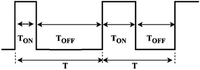
In PWM, a consistent frequency is maintained while voltage control is achieved by adjusting the duty cycle. This is the prevailing method for voltage control. In this approach, power is periodically switched on during fixed cycles to extract the required output power from the input. The waveform of PWM is shown in Fig. 3.
Fig. 3.
PWM waveform.
The total period can be calculated by,
| T = TON + TOFF | (4) |
where T is the total period, TON represents on time and TOFF represents off time, respectively.
The benefit of PWM control is its ability to predict switching noise due to its fixed frequency, simplifying the filtering process. However, a limitation of this approach is that the number of switching operations remains constant regardless of the load, leading to a consistent self-consumption current. Consequently, during light loads, switching loss becomes dominant, significantly reducing efficiency.
3.2. PFM control
PFM functions by maintaining a constant pulse on time while adjusting control through the modulation of the off-time. There are two types of PFM: fixed-on time and fixed-off time. In the fixed-on time type, for instance, the on-time remains constant while the off-time can be adjusted, as illustrated in Fig. 4.
Fig. 4.

PFM waveform.
The PFM technique upholds high efficiency even under light loads. During light load operation, minimal power supplementation is necessary, resulting in a lowered switching frequency and fewer required switching actions, thereby decreasing switching losses. The main drawback of this technique is that, due to frequency variation, the switching noise remains unpredictable, complicating filtration control and making noise removal more difficult.
3.3. PSM control
PSM serves as another variable frequency modulation technique specifically designed for light-load operations. In this control, the switch is activated or deactivated only when required to maintain output voltage regulation. This strategy decreases the frequency of switching cycles, leading to lower switching losses compared to continuous switching methods. By omitting unnecessary pulses, PSM efficiently minimizes energy dissipation during periods of light load. However, implementing PSM can incur costs due to the necessity for specialized control components and precise timing mechanisms. Despite its effectiveness in reducing switching losses at light loads, PSM does not eliminate them.
4. Literature survey of control methods for highly efficient buck converters
The control of buck converters encompasses a diverse range of techniques rather than relying on a singular approach. Various methodologies can be integrated to optimize efficiency significantly. However, the primary objective of this paper is to elucidate the foremost technique employed by researchers in controlling buck converters specifically tailored for IoT applications. The control method primarily emphasizes the following divisions. It comprises the PSM, PFM, PWM, AOT, Hysteretic, Hybrid, Tri-mode and digital PWM. These methods are based on additional controllers with synchronous buck converter. In this study, control and modulation methods for buck converters to IoT applications are reviewed.
4.1. Adaptive pulse skip modulation (APSM) buck converter
The APSM buck converter, as presented in Ref. [2], seeks to attain adaptive functionality marked by superior conversion efficiency and minimal quiescent current. This methodology places particular emphasis on augmenting dynamic range while minimizing output ripple through the utilization of a hybrid control strategy, which concurrently governs both the pulsation frequency and the on-time period.
The DDBC illustrated in Fig. 5 proposed by Ref. [2], integrates an adaptive frequency modulator and an AOT controller. Upon system power-up, the on-chip relaxation oscillator initiates clock signal generation. At the rising edge of the clock signal, the latched comparator compares the output voltage with VREF. If the output voltage is lower than VREF, the gating signal is produced by the output regulator. Simultaneously, the clock frequency increases by accumulating the frequency modulating register [FMR]. When FMR remains at 11 for three consecutive periods, the on-time period extends by accumulating the pulse width modulating register, resulting in a higher peak inductor current. This process continues until output voltage exceeds VREF, upon which the gate signal is set to 0 to skip the entire switching period. Due to this, the switching frequency decreases and the on-time period is reduced. This adaptive control strategy allows the converter to adapt to varying load conditions. Indeed, the proposed converter is designed to optimize efficiency at light loads by operating at lower frequencies. However, as the load reaches its maximum, the efficiency tends to decrease.
Fig. 5.

Diagrammatic representation of APSM [2].
4.2. Low-ripple-voltage PFM buck converter
Fig. 6 illustrates a novel PFM buck converter featuring low ripple voltage and integrated with a dynamic compensator, as proposed by Ref. [86]. In conventional setups employing a static compensator with a PFM BC, a notable shoot-through current is present, impacting the converter's light load efficiency [87]. The proposed converter resembles that of a PFM BC with a static comparator. when inductor current (IL) reaches zero, the zero-current detector triggers a ZC signal to go HIGH, deactivating MN. Consequently, VOUT diminishes as COUT supplies all necessary charges for ILOAD. As VOUT drops below the target level, the dynamic comparator sets CMP HIGH during the rising edge of the clock (CLK), activating MP. Notably, because the dynamic comparator only functions at the CLK edge, the maximum output voltage error (Verr) is contingent on the clock frequency [[44], [45]]. By increasing the clock frequency, the error voltage can be reduced. A dynamic shutdown control method is used to minimize controller losses, selectively deactivating unnecessary control circuits. When the high-side switch is ON and the inductor current increases, only peak current detection is needed, so the zero-current detector and dynamic comparator are turned OFF. As the low-side switch turns ON and the inductor current decreases to zero, only the zero-current detector is necessary, leading to the deactivation of the peak current detector and dynamic comparator. when all power switches are OFF and the inductor current remains at zero, only the output voltage level requires detection, resulting in the deactivation of the peak current detector and zero-current detector. By selectively turning off control circuits, the proposed design minimizes controller loss even at low ripple voltages. The dynamic comparator and shutdown control add complexity to the design, which may impact manufacturing and reliability.
Fig. 6.

PFM buck converter with low ripple voltage [86].
4.3. Tri-mode buck converter
The modified tri-mode buck converter, as depicted in Fig. 7, has been introduced by Ref. [87] and operates based on events to conserve power consumption in clock generation. However, to ensure proper startup, it requires a specific initial state. If the initial voltage (VO) is close to zero and GD H is high, the AOT comparator may fail to produce a definite output, potentially trapping the converter in an off-time state and preventing the first on-time initiation. To circumvent this issue, an OR gate is placed ahead of the RS trigger, ensuring correct system startup and avoiding erroneous initial states. Moreover, for extremely light loads, minimizing quiescent current and control circuitry power consumption is crucial. To address this, a novel deep green mode (DGM) with ultra-low quiescent current is introduced. This innovation enhances power efficiency and expands the load range down to 1 μA, catering to the requirements of power-sensitive applications. To enhance power efficiency at light loads, the DGM incorporates various power-saving strategies at both system and circuit levels. At the system level, the DGM's control scheme shuts down the EA entirely and biases the comparator with a lower current to minimize power consumption. Additionally, the intentionally prolonged delay of the comparator (TD) resulting from the low bias current is utilized to create a load-dependent hysteresis window, thereby reducing the switching frequency. At the circuit level, the zero-crossing detector (ZCD) and AOT comparator are dynamically biased, effectively reducing average quiescent current while maintaining comparison speed. These integrated techniques optimize power consumption across the system, ensuring efficient operation even under light load conditions.
Fig. 7.

Diagrammic representation of Tri mode buck converter [87].
The proposed tri-mode converter [49], is depicted in Fig. 8, incorporates a load current prediction scheme for enhanced performance. It comprises components such as a sawtooth oscillator that is controlled by voltage (VCSO), mode selector, n divider, and low-pass filter. The VCSO generates VSAW and SET with a variable switching frequency determined by VF. The mode selector dictates operational modes based on average error voltage (Verr)status and adjusts forward voltage (VF) to provide load-dependent switching frequencies. In PFM mode, VF links to Verr, while in PWM or Multiple saw-tooth (MSPWM) modes, fixed VPFM or VMSPWM L is connected, respectively. A multiplexer in the mode selector facilitates smooth transitions between MSPWM and PFM modes. In MSPWM mode, the n divider generates multiple sawtooth waveforms. Upon initial power-up, a soft-start sequence mitigates in-rush current, safeguarding the converter and battery. During soft-start, the compensator is inactive, and the output voltage gradually rises with constant on-time (COT) operation. Once the feedback voltage (VFB) signals reach the reference voltage (VREF), it enables the loading circuits to engage. The compensator activates, and the converter selects appropriate operational modes based on load conditions.
Fig. 8.

Buck converter with load protection scheme [49].
4.4. Buck converter with A2-Comparator and sleep-time detector under AOT control
The modified minima-power AOT-controlled BC, illustrated in Fig. 9 introduced by Ref. [5], operates with a quasi-fixed switching frequency in the continuous conduction mode (CCM). Utilizing the AOT control topology [[88], [89], [90]], the converter exhibits PFM control characteristics in the DCM mode during light load conditions, resulting in enhanced efficiency [91]. The current through the inductor (IL) is monitored and converted into a voltage signal (VSEN) by an on-chip current sensor (RS and CS), which runs parallel to the output inductor (L). This method is commonly employed in ripple-based AOT control, where a ceramic capacitor with minimal equivalent series resistance RESR is utilized. Additionally, a voltage feedback loop, comprising internal feedback resistors (RFB1 and RFB2), generates the feedback voltage signal (VFB). This loop, facilitated by an error amplifier (EA) and A2-comparator, maintains converter accuracy and minimizes output ripple across varying loads. To ensure stability, an on-chip compensator (RC and CC) is employed. Charging time (TON) is adaptively generated by an ON-time generator based on the difference between input (VIN) and output (VOUT) voltages. Switching frequency is determined by comparing VSEN with an error signal (VE) in the A2-comparator. Zero-current detection (ZCD) prevents reverse current flow post-discharge, thus enhancing system efficiency. The converter's quiescent current can be significantly reduced to the order of hundreds of nanoamperes under light load conditions [92]. To discern the transition between light load and ultralight load, an inactive time detector circuit is employed [93]. The attainment of reduced power consumption is facilitated through the incorporation of adaptive gain (A2) comparators and adaptive bias. The control logic block generates signals (PWM P and PWM N) to control power transistor states (MN and MP), while the dead-time controller inserts a dead time to prevent simultaneous activation of MN and MP.
Fig. 9.

AOT controlled buck converter with A2-comparator [5].
4.5. Buck converter under DCT/PWM control
The research presented in Ref. [18] introduces a novel control technique termed ”Double Clock Time” (DCT) for inductive-based DC-DC converters, incorporating a digital current sensor depicted in Fig. 10. It utilizes DCM and PWM control. The system includes a buck converter with power inductor and output capacitor, DCT and PWM control blocks, bandgap reference with low dropout regulators (LDOs), zero current detection (ZCD) control, mode selection, level-shifter, gate drivers, and feedback resistor networks. The converter primarily operates in DCM for sleep, standby, and transmit modes, employing a type II compensator for PWM control. During low power modes, PWM control is turned off to reduce consumption. An Adaptive ZCD power supply minimizes ZCD control power consumption. LDOs maintain stable supply voltages for control circuits, minimizing sensitivity to input voltage variations. The bandgap reference and LDOs enable thin-oxide transistor usage, reducing the quiescent current. Different output voltages are set using feedback resistor networks. The proposed methodology alleviates the complexity of the control circuit in comparison to the conventional tri-mode control elucidated in Refs. [[17], [18], [19]]. Overall, the system optimizes power efficiency and consumption for IoT devices.
Fig. 10.

DCT/PWM Control buck converter [18].
4.6. Hybrid synchronous and asynchronous loop control in a buck converter
Conventional approaches necessitate a high-frequency clock in the megahertz range and primarily target a milliwatt power range, rendering them unsuitable for ultralow power applications. To overcome these challenges [3], introduces a sub-nanowatt (sub-nW) buck converter, as illustrated in Fig. 11, featuring high peak efficiency, a broad dynamically adjusting voltage and frequency (DAVF) and frequency-locked time reference (FLTR).
Fig. 11.

Integrated synchronous and asynchronous loop control based buck converter [3].
The architecture is divided into four main components, including a power stage with off-chip components, a synchronous pulse frequency modulation (PFM) loop, an asynchronous control loop, and a pulse generator with drivers, the system regulates power delivery from input (VIN) to output (VOUT). The synchronous PFM loop regulates the buck converter's output by comparing VOUT and a reference voltage (VREF), enabling power delivery if VOUT is lower than VREF. The frequency controller adjusts the clock frequency adaptively to maintain a specific ratio. The mode controller switches between synchronous, DAVF, and FLTR modes, activating the asynchronous loop when necessary for faster response. Unlike traditional methods, the asynchronous loop generates pulses to regulate the output through the synchronous loop. It utilizes the continuous-time comparator (CT) to detect voltage droops, generates pulses for DAVF and FLTR, selects the appropriate clock, and provides a feedforward signal for quick response. This design optimizes power efficiency and area while achieving rapid reference tracking for DAVF and FLTR [94]. The converter effectively mitigates static power through the implementation of a robust driver, digitalization, length split technique, signal recycling, and path multiplexing distinguishing it from alternative methods [28,[95], [96], [97], [98]].
4.7. Two-Stage DPWM and low-power Self-Adjusting zero current detection in a buck converter
The DPWM buck converter architecture depicted in Fig. 12 proposed by Ref. [64] comprises several key components: a hybrid DPWM core, adaptive window ADC, digital ST-ZCD, type-III digital compensator, power stage, and gate driver. The adaptive window ADC takes feedback voltage (VFB) from the output (VOUT) and provides signals for duty information to the digital compensator. This compensator, employing Tustin's method [99], minimizes current consumption and area while ensuring proper phase margin and crossover frequency in the digital domain. The hybrid DPWM core combines counter-based and delay line methods to achieve high linearity and low power consumption, enabling a wide delay control range with fine resolution. Despite operating with a 6-bit resolution for reduced power dissipation and area, the converter mitigates high output voltage ripple through the adaptive window ADC, which dynamically selects input range based on VFB to maintain ripple within 20 mV. The ST-ZCD replaces conventional dead-time generators, minimizing power consumption by sensing duty pulses without comparators and preventing reverse currents. Under a 10-mA load current, the proposed DDBC achieves noteworthy performance, featuring a reduced capacitor value and die area when compared to alternative designs [64,100].
Fig. 12.

Two-stage DPWM and low-power self-adjusting ZCD in a buck converter [64].
This integrated design enhances power conversion efficiency while reducing output voltage ripple and power dissipation, making it suitable for low-power applications.
4.8. AOT control for a buck converter with Two-Dimensional Operation
The single-inductor dual-input dual-output (SIDIDO) DDC proposed by Ref. [101], illustrated in Fig. 13, integrates converter switches, voltage reference, dual-output regulation, and input source management. It supports two output voltages, VOUT1 and VOUT2, catering to energy-efficient digital circuits and a low-voltage RF transmitter, respectively. VOUT1 is regulated between 0.4 V and 0.6 V, while VOUT2 operates within the 1–1.2 V range, storing excess energy. The proposed 2-D AOT system is composed of a tunable delay chain, a comparator-based ADC with a digital controller, and a bias generator. In contrast, the COT configuration consists of a constant delay circuit and a D -Flip flop (FF) [102]. The utilization of the modified sequential pulse-skipping modulation (SPSM) technique [103] facilitates efficient regulation of the two output voltages, replacing the conventional sequential control that relies on compensation circuits [104]. Power stages utilize non-inverting buck-boost and buck modes for flexible and efficient voltage conversion [105]. This design ensures flexible voltage conversion with high efficiency under diverse input and output voltage conditions [[106], [107], [108], [109]]. Clock generation ensures proper internal clock signals, while latch-type comparators compare divided voltages with a reference from a low-power bandgap reference. Maximum power point tracking (MPPT) optimizes energy extraction from photovoltaic (PV) cells, with mode detection automatically adjusting input energy source and charging outputs. 2-D AOT controls on-time periods for power switches to reduce output ripple, while ST-ZCD manages off-time periods to prevent reverse inductor current. The SPSM block governs output charging priority, ensuring voltage regulation with minimal cross-regulations.
Fig. 13.

Aot control for a buck converter with two-Dimensional operation [101].
4.9. Double-mode buck converter with digital control and pulse skipping detection
Fig. 14 illustrates the architecture of the proposed DDBC by Ref. [110], comprising a load detector,pulse-skipping adaptive on-time (PSAOT) control circuit, pulseskipping asynchronous mode (PSAM) control circuit, zero current detectors (ZCD) and dynamic comparator with adjustable offset. Both PSAM and PSAOT modes operate in DCM mode for improved loop stability. All circuits have implemented power gating to minimize static power, with mode selection determined by the load detector, which is the primary source of power reduction in ultra-light loads. The load detector employs pulse-skipping load detection, enhancing transient response with speed-up mechanisms. An adjustable offset comparator provides additional load information by modifying the reference voltage. Mode transitions are facilitated to maximize duty and accelerate recovery time based on load conditions. Hysteresis windows aid in mode selection, with PSAOT and PSAM modes enabled depending on load characteristics. output voltage ripple and Loop stability are ensured by maintaining a stable DCM operation [111], where the voltage feedback remains higher than the reference voltage, preventing subharmonic oscillations. The converter is stable within the required dynamic range, effectively mitigating output voltage ripple.
Fig. 14.

Double-mode buck converter with digital control and pulse-skipping load detection [110].
5. Comparative analysis and discussions
Based on the need for input and output power requirements by the system, the selection of appropriate control methods can be considered. In Table 1, a comparison of various control modes for a high-efficiency DDBC is given. It includes APSM, PFM, MSPWM, AOT, DCT, DPWM,2D-AOT and PSAM. Each method of the selected high-efficiency DDBC has its characteristics, merits and demerits. Table 1 presents the comparison of each method based on input voltage, output voltage, efficiency, quiescent current, and output ripple. The efficiency of DDBC can be given as [112],
| (5) |
| PD = PL + PFET + OL | (6) |
where η is the converter efficiency, Po is the output power, PD is the dissipated power, PFET is the MOSFET loss, and OL denotes other losses.
Table 1.
Comparative analysis of buck converter with its performance parameters, area, and cost.
| S.NoRef.No | Technology | Input (V) | Output (V) | Quiescent current/power | Output ripple (mV) | Peak Efficiency (%) | Efficiency (%) @ light load | Control Mode | Die Area (mm2) | Estimated Cost |
|---|---|---|---|---|---|---|---|---|---|---|
| 1 [2] | 180 nm | 2.4-3.6 | 0.6-1.5 | 8 nA | 15 | 96 | 80 | APSM | 0.56 | Low |
| 2 [3] | 65 nm | 1.5-2.3 | 0.5-0.9 | 0.801 nW | 92 | 93 | 80 | PFM/LM/PWM | 0.237 | Moderate |
| 3 [5] | 0.18 μm | 2.1–5.5 | 1.8 | 240 nA | 19 | 90.04 | 95.8 | AOT | 1.092 | Low |
| 4 [6] | 130 nm | 1.8-3.3 | 1.2 | 0.44–12.32 nA | 29 | 92.15 | 87.7 | Hysteretic | 0.14 | Moderate |
| 5 [17] | 180 nm | 0.55-1.0 | 0.35-0.5 | 145 nA | <10 | 92 | 47 | AM + PFM + PWM | 1.44 | Low |
| 6 [18] | 180 nm | 2.0–5 | 0.8–3 | 470 nA | 15 | 93 | 85.6 | DCT + PWM | 1.1 | Low |
| 7 [19] | 0.13 μm | 2.2–3.3 | 1.7 | 500 nA | 180 | 92.4 | 81.2 | RM + PFM + PWM | 0.656 | Moderate |
| 8 [20] | 0.18 μm | 2.5–5.5 | 1.15-1.8 | 50 μA | 30 | 91 | – | PWM/ABM | 3.2 | Low |
| 9 [26] | 180 μm | 3–5 | 1.8–12 | 217 nA | 31 | 86 | 55 | PSM | 1.8 | Low |
| 10 [28] | 65 nm | 1.2–3.3 | 0.7-0.9 | 400 pw-0.8 nw | 10 | 92 | 30 | PFM | 0.32 | Moderate |
| 11 [28] | 65 nm | 1.2–3.3 | 0.7-0.9 | 0.2 nA | 10 | 92 | 70 | PSM | 0.32 | Moderate |
| 12 [86] | 0.35 μm | 2.7-4.2 | 1.2-1.8 | 15.5–2.8 μA | 3 | 92.8 | 80.6 | PFM | 0.5304 | Low |
| 13 [87] | 0.18 μm | 2.7-4.7 | 1.6 | 490 nA | 50 | 92.1 | 51.3 | PWM + PFM + DGM | 0.55 | Low |
| 14 [47] | 45 nm | 2.8-4.2 | 0.4-1.2 | – | 20 | 87 | 71 | PFM + PWM | 0.11 | High |
| 15 [49] | 0.18 μm | 2.0–3.3 | 1.2 | – | 15 | 91 | 48 | PWM + PFM + MSPWM | 0.14 | Low |
| 16 [64] | 55 nm | 1.5–3 | 1.2 | 130 μA | 20 | 91.5 | 54 | DPWM | 0.15 | Moderate |
| 17 [101] | 40 nm | 0.5-1.4 | 0.4-1.2 | – | 20 | 92.5 | 80 | SPSM | 2.415 | High |
| 18 [110] | 350 nm | 4.2–5 | 3.3 | 180 nA | 16 | 92.9 | 84 | PSAOT + PSAM | 3.78 | Moderate |
| 19 [113] | 90 nm | 1.8-4.2 | 0.9-1.4 | 12 μA | 20 | 85.6 | 78 | PFM | 3.375 | Moderate |
| 20 [114] | 28 nm | 1.80 | 0.4-1.4 | 262 nA | 30 | 89 | 55 | PWM/PSM | 0.5 | High |
| 21 [115] | 0.18 μm | 2.9-3.3 | 1.1–1.7 | – | 10 | 93.2 | – | DPWM | 0.6 | Low |
| 22 [116] | 0.18 μm | 2.5-3.3 | 1 | – | 240 | 86.5 | 71 | PWM | 0.375 | Low |
| 23 [117] | 0.25 μm | 1.2–2.5 | 1 | 181 nA | <30 | 95 | <70 | DOOT | 0.5 | Low |
∗RM- Retention mode ∗DOOT-Dynamic on/off time.
equations (5), (6) include output power loss, inductor conduction loss, MOSFET conduction loss, switching loss, and quiescent losses. Table 1 presents a comparison of each method based on performance parameters such as input voltage, output voltage, efficiency, quiescent current, and output ripple. The converters have different CMOS fabrications and various control modes. Thus, a buck converter with a specific input and output voltage range is taken for discussion.
5.1. Analysis of quiescent current (Iq)f the reported DDC buck converters
Quiescent current refers to the current drawn by an integrated circuit (IC) when it is active but not actively switching, or when no load is present. While the converter consumes more current at no load conditions, it leads to an increase of power loss. The total loss accompanies quiescent loss and based on it; the efficiency calculation is done. The articles [2,26,28] used PSM control to reduce the Iq and the APSM-based BC [28] achieved a very low quiescent current that is 0.2 nA. The amount of quiescent current consumed in the proposed BC [64] is 130 μA which operates in DPWM mode. It is considerably higher than other modes of operation. The DDBC with PFM and PWM control [5,6,[17], [18], [19],87,49,114,117] achieved in the range of nA. The articles [3,28] propose the converter has low quiescent losses that are measured in nW. Under the conditions of light load, the efficiency is notably reduced due to the substantial quiescent current. The PSM technique can be used to improve the efficiency by reducing the quiescent loss.
5.2. Analysis of output ripple of the reported DDC buck converters
The output ripple voltage within a power converter denotes the oscillations or deviations present in the output voltage waveform. These variations overlay the constant DC output voltage and can induce significant impacts, including performance deterioration, transient response issues, electromagnetic interference (EMI), efficiency concerns, and challenges with filtering and decoupling. In certain standard DC-DC converters, the regulation of the output voltage is commonly achieved through the application of control techniques such as PWM and PFM [20,21]. In certain standard DC-DC converters, the regulation of the output voltage is commonly achieved through the application of control techniques such as PWM and PFM [118,119]. The article [86] proposed a PFM buck converter that has a low output voltage ripple of 3 mV. Although the converters [3,5,6,[18], [19], [20],87,47,49,64,101,114,117] achieved good efficiency, they suffer from the high output voltage ripple which is greater than 10 mV. The DDBC [19] operates in PWM and PFM modes and has a more output voltage ripple of 180 mV. It is comparatively higher than other control mode of operation. The proposed adaptively controlled PSM BC [86] has a very minimum output ripple voltage compared with other PFM BC [19,87,49]. Voltage ripple in battery-powered systems significantly influences the longevity of batteries. The repeated charging and discharging cycles induced by ripple can lead to a reduction in the overall lifespan of the battery. Therefore, PFM Buck converters can be chosen for battery-powered applications to achieve low ripple voltage.
5.3. Analysis of the efficiency of the reported DDC buck converters
The selection of a suitable control mode plays a vital role in improving the efficiency of DDBC. The proposed converter [2] based on adaptively controlled PSM mode operation has achieved a peak efficiency of 96 % compared to other converters [26,28]. Even though the PFM converters [19,86,87,47,49,113] have achieved more than 90 % peak efficiency, it suffers from the problem of low light load efficiency. The APSM BC [2] attains more than 70 % of efficiency at light load conditions. The PWM-based DDC buck converters [[17], [18], [19],47,116] achieve peak efficiency which is more than 90 % but it will not be suitable for light load applications. The proposed converters [64,114,115] operate in DPWM and only provide low light efficiency due to high quiescent current [64]. Achieving good light load efficiency is essential in DDBC for battery-powered IoT applications. PSM and PSM mode can help the converter achieve acceptable light load efficiency to enhance battery life.
5.4. Features
This literature study revealed that the most predominant parameters for highly efficient DDBC are input voltage, voltage ripple, quiescent current, and control mode. The researchers could identify that according to these parameters, the performance of DDBC is varied in terms of efficiency. The features of control modes are represented in Table 2. It gives peak efficiency, pros and cons of APSM. PFM, Tri-mode, AOT, DCT/PWM, Hybrid, DPWM, 2-D AOT, PSAOT, LADRC and PCM [120].This suggests that certain control modes for the converters have achieved high efficiency over 90 % and provides good stab. From these, the researcher can choose control modes depending on their features in real-time applications.
Table 2.
Features of various control modes.
| Control mode | Peak efficiency (%) | Pros and Cons |
|---|---|---|
| APSM | 96 | Adaptive control optimizes efficiency across varying loads, enhancing overall performance. But support only single output. |
| PFM | 93.4 | The controller loss is significantly reduced by a PFM buck converter, even when operating at low output ripple voltages. EMI interference is not considered. Using a dynamic comparator enhances voltage gain and evaluation speed, reducing power consumption. |
| Tri-mode | 92.1 | The converter achieves an ultra-low quiescent current, making it suitable for energy-efficient IoT devices. It may involve trade-offs regarding transient response time or voltage ripple; Researchers need to balance these factors to optimize overall performance carefully. |
| AOT | 95.8 | Using an adaptive bias and adaptive gain comparator improves loop stability; mitigating issues caused by propagation delays in low-power comparators. Low efficiency in ultra-light load conditions because of the relatively large quiescent current. |
| DCT/PWM | 94.7 | The dual-mode operation allows for flexibility in managing different load conditions. The efficiency suffers under ultra-light load conditions due to the comparatively high quiescent current. A load current detector consumes significant power. |
| Hybrid | 93 | Enabling efficient power management by adjusting voltage and frequency based on workload demands. Managing voltage droop effectively is critical for maintaining stable operation. |
| DPWM | 91.5 | The hybrid DPWM core combines high linearity and low power consumption. It utilizes a two-step delay control using counters and delay lines, allowing efficient switching between modes. The response time for mode transitions and adjustments should be considered to avoid performance degradation. |
| 2-D AOT | 94 | 2-D AOT technique improves dual-source conversion efficiency across a wide input voltage range. Integrating dual input sources and adaptive control techniques can increase circuit complexity. |
| PSAOT | 92.9 | An adjustable offset is employed to accelerate the transient response during load changes. Despite the pulse-skipping modes, there may still be some output voltage ripple under different load conditions. Trade-offs: Balancing efficiency, transient response, and simplicity requires careful consideration. |
| LADRC | – | More effective in reducing output voltage fluctuations caused by power supply variances and load switching disturbances. Because of its complexity, implementing LADRC in hardware may necessitate additional expertise and resources. |
| PCM | – | The integration of a circuit that has slope-compensation adjustment naturally ensures stability in terms of subharmonic oscillation. Integrating circuitry for sensing the input-to-output conversion ratio and adjusting the adaptive slope increases the complexity of the entire system. |
∗PCM-Peak current mode.
6. Future direction
Power management circuits play an important role in IoT applications. The efficiency of DDBC is decided by various parameters such as quiescent loss, output ripple, and control modes of operation. Choosing a suitable modulation technique and designing a control method is crucial to achieve high efficiency. Most IoT applications are battery powered devices that require battery longevity. To increase the battery lifetime, the design of an efficient buck converter with a suitable control mode is necessary. In the last few years, many control techniques have been developed and implemented in DDBC. Despite the latest control techniques having several advantages, there is an improvement is imperative in the reduction of output ripples, and a quiescent current is required. From the researcher's point of view, more control techniques have to be discovered depending on the existing methods. We anticipate that the thorough overview of modulation and control methods presented in this paper will serve as a foundational resource for future exploration and innovation in the field. Moving forward, control methods are expected to progress notably in the following domains.
-
1.
Despite the considerable advancement of controlling techniques, there is still anticipation for the emergence of novel control techniques. Given that the existing control methods fail to address the quiescent loss experienced by certain converters in light load conditions.
-
2.
Frequency stabilization during load transient and voltage transient is a major problem in DDC buck converters. Although many researchers proposed compensation circuits for the frequency variation, circuit complexity is still available. So, additional research on the light load application of the control method is imperative.
-
3.
Despite the existing control methods for DDC buck converters in IoT applications, there hasn't been sufficient attention and research dedicated to control methods for other DDC converters (such as boost converters, buck-boost converters, and flyback converters) and applications. Thus, advanced control modulation techniques or procedures should be thoroughly researched for DDC buck converters and all other DDC converters, based on modern control theory methods and switching behaviour modulations.
7. Conclusion
In the analysis of various control methods for high-efficiency DDBC, it is evident that different modes offer unique advantages and limitations based on specific performance parameters such as input voltage, output voltage, efficiency, quiescent current, and output ripple.
-
1.
Quiescent Current: The quiescent current is crucial as it affects the efficiency during no-load conditions. Techniques like PSM have been effective in reducing quiescent current, with APSM-based converters achieving as low as 0.2 nA. Conversely, the DPWM mode reported a relatively high quiescent current at 130 μA.
-
2.
Output Ripple: Output ripple impacts performance and battery longevity. FM buck converters are preferable for applications requiring low ripple, with some achieving as low as 3 mV. However, many converters operating in PWM and PFM modes have higher ripples, exceeding 10 mV, which is detrimental in battery-powered systems.
-
3.
Efficiency: Peak efficiency varied across different control modes. APSM achieved the highest at 96 %, demonstrating superior performance in varying load conditions. PFM converters consistently achieved over 90 % peak efficiency but struggled with light load efficiency. PWM-based converters also exceeded 90 % peak efficiency but were less effective for light load scenarios due to higher quiescent currents.
In summary, while PSM and APSM modes show promise in achieving low quiescent currents and high efficiencies, especially under light loads, PFM is beneficial for low ripple applications. PWM modes, although efficient at peak load, are less suitable for light load conditions. Therefore, selecting an appropriate control mode should be based on the application's specific requirements, balancing efficiency, quiescent current, and output ripple considerations. This study is intended to serve as a reference for designing and constructing a new control method for a non-isolated synchronous DDBC. In the future, researchers will be able to select and integrate the right control method for the needs of IoT applications.
Data availability statement
No data was used for the research described in the article.
CRediT authorship contribution statement
Sivakumar Kumaraguruparan: Writing – original draft, Validation, Software, Resources, Methodology, Investigation, Formal analysis, Data curation, Conceptualization, Visualization. Konguvel Elango: Supervision, Formal analysis, Investigation, Validation, Writing – review & editing.
Declaration of competing interest
The authors declare that they have no known competing financial interests or personal relationships that could have appeared to influence the work reported in this paper.
Contributor Information
Sivakumar Kumaraguruparan, Email: sivakumar.k2022@vitstudent.ac.in.
Konguvel Elango, Email: konguvel.e@vit.ac.in.
References
- 1.Mao F., Lu Y., Lin J., Zhan C., Seng-Pan U., Martins R.P. Proc. IEEE Int. Symp. Circuits Syst. (ISCAS) May.2018. A single-stage current-mode active rectifier with accurate output-current regulation for IoT; pp. 1–4. Florence, Italy. [DOI] [Google Scholar]
- 2.Gao Z., Hao Y., Wei H., Li Y., Chen M. A 96% peak efficiency adaptively controlled PSM buck converter with low-quiescent current and wide dynamic range for IoT applications. IEEE Solid State Circuits Lett. 2022;5:276–279. doi: 10.1109/LSSC.2022.3222879. [DOI] [Google Scholar]
- 3.Liu X., Calhoun B.H., Li S. A sub-nW 93% peak efficiency buck converter with wide dynamic range, fast DVFS, and asynchronous load-transient control. IEEE J. Solid State Circ. 2022;57(7):2054–2067. doi: 10.1109/JSSC.2022.3161617. Apr.2022. [DOI] [Google Scholar]
- 4.Gao Z., Chen M., Liu K., Zhao J., Li Y., Wang G. An asynchronous ACDC boost converter with event-driven voltage regulator and 94% efficiency for low-frequency electromagnetic energy harvesting. IEEE Transactions on Circuits and Systems II: Express Briefs. Jul. 2021;68(7):2563–2567. doi: 10.1109/TCSII.2021.3055949. [DOI] [Google Scholar]
- 5.Huang W., Liu L., Liao X., Xu C., Li Y. A 240-nA quiescent current, 95.8% efficiency AOT-controlled buck converter with A2-comparator and sleep-time detector for IoT application. IEEE Trans. Power Electron. Nov. 2021;36(11):12898–12909. doi: 10.1109/TPEL.2021.3082896. [DOI] [Google Scholar]
- 6.Santoro F., et al. A hysteretic buck converter with 92.1% maximum efficiency designed for ultra-low power and fast wake-up SoC applications. IEEE J. Solid State Circ. Jun. 2018;53(6):1856–1868. doi: 10.1109/JSSC.2018.2799964. [DOI] [Google Scholar]
- 7.Mao F., Lu Y., Martins R.P. A reconfigurable cross-connected wireless-power transceiver for bidirectional device-to-device wireless charging. IEEE J. Solid State Circ. Sep. 2019;54(9):2579–2589. doi: 10.1109/JSSC.2019.2921449. [DOI] [Google Scholar]
- 8.Jiang Y., Law M.K., Chen Z., Mak P.I., Martins R.P. Algebraic SeriesParallel-based switched-capacitor DC-DC boost converter with wide input voltage range and enhanced power density. IEEE J. Solid State Circ. Nov. 2019;54(11):3118–3134. doi: 10.1109/JSSC.2019.2935556. [DOI] [Google Scholar]
- 9.Jiang Y., Law M.K., Mak P.I., Martins R.P. Algorithmic voltage-feed-in topology for fully integrated fine-grained rational buck-boost switched-capacitor DC-DC converters. IEEE J. Solid State Circ. Dec. 2018;53(12):3455–3469. doi: 10.1109/JSSC.2018.2866929. [DOI] [Google Scholar]
- 10.Li Y., Zhu Z. A capacitor-free control scheme for a primary-side controlled flyback converter. IEEE Trans. Power Electron. Sep. 2020;35(9):9484–9495. doi: 10.1109/TPEL.2020.2973124. [DOI] [Google Scholar]
- 11.Kim J.H., Kim J.K., Lee J.B., Moon G.W. Load Adaptive gate driving method for high efficiency under light-load conditions. IEEE Trans. Ind. Electron. 2014;61(9):4674–4679. doi: 10.1109/TIE.2013.2290777. [DOI] [Google Scholar]
- 12.Hong X.E., Wu J.F., Wei C.L. 98.1%-Efficiency hysteretic-current-mode noninverting buck-boost DC-DC converter with smooth mode transition. IEEE Trans. Power Electron. Mar. 2017;32(3):2008–2017. doi: 10.1109/TPEL.2016.2567484. [DOI] [Google Scholar]
- 13.Liou W.R., Yeh M.L., Kuo Y.L. A high efficiency dual-mode buck converter IC for portable applications. IEEE Trans. Power Electron. Mar. 2008;23(2):667–677. doi: 10.1109/TPEL.2007.915047. [DOI] [Google Scholar]
- 14.Li Y., Zhu Z. A constant current control scheme for PrimarySide controlled flyback controller operating in DCM and CCM. IEEE Trans. Power Electron. Sep. 2020;35(9):9464–9472. doi: 10.1109/TPEL.2020.2972771. [DOI] [Google Scholar]
- 15.Kim S.J., Choi W.S., Pilawa-Podgurski R., Hanumolu P.K. A 10-MHz 2800-mA 0.5-1.5-V 90% peak efficiency time-based buck converter with seamless transition between PWM/PFM modes. IEEE J. Solid State Circ. Mar. 2018;53(3):814–824. doi: 10.1109/JSSC.2017.2776298. [DOI] [Google Scholar]
- 16.Huang H.W., Chen K.H., Kuo S.Y. Dithering skip modulation, width and dead time controllers in highly efficient DC-DC converters for system-on-chip applications. IEEE J. Solid State Circ. Nov. 2007:2451–2465. doi: 10.1109/JSSC.2007.907175. [DOI] [Google Scholar]
- 17.Chen P.H., Wu C.S., Lin K.C. A 50 nW-to-10 mW output power TriMode digital buck converter with self-tracking zero current detection for photovoltaic energy harvesting. IEEE J. Solid State Circ. Feb. 2016;51(2):523–532. doi: 10.1109/JSSC.2015.2506685. [DOI] [Google Scholar]
- 18.Zeng W.L., et al. A 470-nA quiescent current and 92.7%94.7% efficiency DCT/PWM control buck converter with seamless mode selection for IoT application. IEEE Transactions on Circuits and Systems I: Regular Papers. Nov. 2020;67(11):4085–4098. doi: 10.1109/TCSI.2020.3006200. [DOI] [Google Scholar]
- 19.Park Y.J., et al. A design of a 92.4% efficiency triple mode control DC-DC buck converter with low power retention mode and adaptive zero current detector for IoT/wearable applications. IEEE Trans. Power Electron. Sep. 2017;32(9):6946–6960. doi: 10.1109/TPEL.2016.2623812. [DOI] [Google Scholar]
- 20.Yuan U.B., Liu M.X., Ng W.T., Lai X.Q. Hybrid buck converter with constant mode changing point and smooth mode transition for high-frequency applications. IEEE Trans. Ind. Electron. Feb. 2020;67(2):1466–1474. doi: 10.1109/TIE.2019.2893826. [DOI] [Google Scholar]
- 21.Shi L.F., Jia W.G. Mode-selectable high-efficiency low-quiescent-current synchronous buck DC-DC converter. IEEE Trans. Ind. Electron. 2014;61(5):2278–2285. doi: 10.1109/TIE.2013.2267697. [DOI] [Google Scholar]
- 22.Lee Tzung-Je, Hsu Chia-Hsin, Wang Chua-Chin. IEEE International Symposium on Circuits and Systems (ISCAS) May.2019. High efficiency buck converter with wide load current range using dual-mode of PWM and PSM; pp. 1–4. [DOI] [Google Scholar]
- 23.Yu G., Chew K.W.R., Sun Z.C., Tang H., Siek L. A 400 nW single-inductor dual-input-tri-output DC-DC buck-boost converter with maximum power point tracking for indoor photovoltaic energy harvesting. IEEE J. Solid State Circ. Oct. 2015;50(11):2758–2772. doi: 10.1109/JSSC.2015.2476379. [DOI] [Google Scholar]
- 24.Kapat S., Mandi B.C., Patra A. Voltage-mode digital pulse skipping control of a DC-DC converter with stable periodic behavior and improved light-load efficiency. IEEE Trans. Power Electron. Apr. 2016;31(4):3372–3379. doi: 10.1109/TPEL.2015.2455553. [DOI] [Google Scholar]
- 25.Sun W., Han C., Yang M., Xu S., Lu S. A ripple control dual-mode singleinductor dual-output buck converter with fast transient response. IEEE Trans Very Large Scale Integr VLSI Syst. Jan. 2015;23(1):107–117. doi: 10.1109/TVLSI.2014.2299873. [DOI] [Google Scholar]
- 26.Yoon K.S., Jung S., Lee J.H., Kim S.J., Kim H.S., Cho G.H. A single-inductor-multiple-output (SIMO) 0.8-V/1.8-V/12-V StepUp/down converter with low-quiescent current for implantable electroceutical SoCs. IEEE Solid State Circuits Lett. Oct.2021;4:182–185. doi: 10.1109/LSSC.2021.3120793. [DOI] [Google Scholar]
- 27.Zhang Shuyu, Zhao Menglian, Bai Xuetong, Yao Yanxia, Wu Xiaobo. IECON 2017-43rd Annual Conference of the IEEE Industrial Electronics Society. Nov.2017. A 6A, 2.5 MHz integrated dual-phase DC-DC buck converter with low quiescent consumption for mobile devices; pp. 497–502. [DOI] [Google Scholar]
- 28.Paidimarri A., Chandrakasan A.P. A wide dynamic range buck converter with sub-nW quiescent power. IEEE J. Solid State Circ. Dec. 2017;52(12):3119–3131. doi: 10.1109/JSSC.2017.2747217. [DOI] [Google Scholar]
- 29.Sahu B., Rincon-Mora G.A. An accurate, low-voltage, CMOS switching power supply with adaptive on-time pulse-frequency modulation (PFM) control. IEEE Transactions on Circuits and Systems I: Regular Papers. 2007;54(2):312–321. doi: 10.1109/TCSI.2006.887472. [DOI] [Google Scholar]
- 30.Arbetter Barry, Maksimovic Dragan. vol. 2. Aug.1997. Control method for low-voltage DC power supply in battery-powered systems with power management; pp. 1198–1204. (PESC97. Record 28th Annual IEEE Power Electronics Specialists Conference. Formerly Power Conditioning Specialists Conference 1970-71. Power Processing and Electronic Specialists Conference 1972). [DOI] [Google Scholar]
- 31.Zhang X., Maksimovic D. Multimode digital controller for synchronous buck converters operating over wide ranges of input voltages and load currents. IEEE Trans. Power Electron. 2010;25(8):1958–1965. doi: 10.1109/TPEL.2010.2043959. [DOI] [Google Scholar]
- 32.Arbetter Barry, Erickson Robert, Maksimovic Dragan. vol. 1. IEEE; Jun.1995. DC-DC converter design for battery-operated systems; pp. 103–109. (Proceedings of PESC’95Power Electronics Specialist Conference). [DOI] [Google Scholar]
- 33.Huang Hong-Wei, Ho Hsin-Hsin, Chen Ke-Horng, Kuo Sy-Yen. Proceedings of the 2006 International Symposium on Low Power Electronics and Design. Oct.2006. Dithering skip modulator with a novel load sensor for ultra-wide-load high-efficiency DC-DC converters; pp. 388–393. [DOI] [Google Scholar]
- 34.Baranwal S.K., Patra Amit, Culpepper Barry. Self oscillating control of a synchronous DC-DC buck converter. 2004 IEEE 35th Annual Power Electronics Specialists Conference (IEEE Cat. No. 04CH37551) Jun.2004;5:3671–3674. doi: 10.1109/PESC.2004.1355125. [DOI] [Google Scholar]
- 35.Zhou S., Rincon-Mora G.A. A high efficiency, soft switching DC-DC converter with adaptive current-ripple control for portable applications. IEEE Transactions on Circuits and Systems II: Express Briefs. Apr. 2006;53(4):319–323. doi: 10.1109/TCSII.2005.859572. [DOI] [Google Scholar]
- 36.Reed Ovens, Chen Mayega, Issa . 2004 Proceedings of the 16th International Symposium on Power Semiconductor Devices and ICs. IEEE; Sep.2004. A high efficiency ultra-deep sub-micron DC-DC converter for microprocessor applications; pp. 59–62. [DOI] [Google Scholar]
- 37.Tsai C.H., Chen B.M., Li H.L. Switching frequency stabilization techniques for adaptive on-time controlled buck converter with adaptive voltage positioning mechanism. IEEE Trans. Power Electron. Jan. 2016;31(1):443–451. doi: 10.1109/TPEL.2015.2405339. [DOI] [Google Scholar]
- 38.Il Seo J., Lim B.M., Lee S.G. A 96.5% efficiency current mode hysteretic buck converter with 1.2% error auto-selectable frequency locking. IEEE Trans. Power Electron. Sep. 2018;33(9):7733–7743. doi: 10.1109/TPEL.2017.2766691. [DOI] [Google Scholar]
- 39.Chen J.J., Hwang Y.S., Chang C.H., Ku Y.T., Yu C.C. A Sub-1 μs fast-response buck converter with adaptive and frequency-locked controlled techniques. IEEE Trans. Ind. Electron. Mar. 2019;66(3):2198–2203. doi: 10.1109/TIE.2018.2833062. [DOI] [Google Scholar]
- 40.Hu K.Y., Lin S.M., Tsai C.H. A fixed-frequency quasi-V2 hysteretic buck converter with PLL-based two-stage adaptive window control. IEEE Transactions on Circuits and Systems I: Regular Papers. Oct. 2015;62(10):2565–2573. doi: 10.1109/TCSI.2015.2466791. [DOI] [Google Scholar]
- 41.Sugahara S., Yamada K., Edo M., Sato T., Yamasawa K. 90% High efficiency and 100-W/cm3 high power density integrated DC-DC converter for cellular phones. IEEE Trans. Power Electron. Apr. 2013;28(4):1994–2004. doi: 10.1109/TPEL.2012.2197762. [DOI] [Google Scholar]
- 42.Wang C., Xu S., Lu S., Sun W. A low-cost constant current control method for DCM and CCM in digitally controlled primary-side regulation flyback converter. IEEE J Emerg Sel Top Power Electron. Sep. 2018;6(3):1483–1494. doi: 10.1109/JESTPE.2017.2779136. [DOI] [Google Scholar]
- 43.Redl R., Sun J. Ripple-based control of switching regulators-An overview. IEEE Trans. Power Electron. 2009;24(12):2669–2680. doi: 10.1109/TPEL.2009.2032657. [DOI] [Google Scholar]
- 44.Wicht B., Nirschl T., Schmitt-Landsiedel D. Yield and speed optimization of a latch-type voltage sense amplifier. IEEE J. Solid State Circ. Jul. 2004:1148–1158. doi: 10.1109/JSSC.2004.829399. [DOI] [Google Scholar]
- 45.Figueiredo P.M., Vital J.C. Kickback noise reduction techniques for CMOS latched comparators. IEEE Transactions on Circuits and Systems II: Express Briefs. Jul. 2006;53(7):541–545. doi: 10.1109/TCSII.2006.875308. [DOI] [Google Scholar]
- 46.Tsai J.C., Huang T.Y., Lai W.W., Chen K.H. Dual modulation technique for high efficiency in high-switching buck converters over a wide load range. IEEE Transactions on Circuits and Systems I: Regular Papers. 2011;58(7):1671–1680. doi: 10.1109/TCSI.2011.2142970. [DOI] [Google Scholar]
- 47.Bandyopadhyay S., Ramadass Y.K., Chandrakasan A.P. 20 μA to 100 mA DC-DC converter with 2.8-4.2 v battery supply for portable applications in 45 nm CMOS. IEEE J. Solid State Circ. Dec. 2011:2807–2820. doi: 10.1109/JSSC.2011.2162914. [DOI] [Google Scholar]
- 48.Xu W., Li Y., Gong X., Hong Z., Killat D. A dual-mode single-inductor dual-output switching converter with small ripple. IEEE Trans. Power Electron. 2010;25(3):614–623. doi: 10.1109/TPEL.2009.2033927. [DOI] [Google Scholar]
- 49.Hong W., Lee M. A 7.4-MHz tri-mode DC-DC buck converter with load current prediction scheme and seamless mode transition for IoT applications. IEEE Transactions on Circuits and Systems I: Regular Papers. Dec. 2020;67(12):4544–4555. doi: 10.1109/TCSI.2020.2995734. [DOI] [Google Scholar]
- 50.Zhang S., Zhao M., Wu X., Zhang H. Dual-phase DC-DC buck converter with lightload performance enhancement for portable applications. IET Power Electron. Apr. 2018;11(4):719–726. doi: 10.1049/iet-pel.2017.0510. [DOI] [Google Scholar]
- 51.Chen Y., Mak P.I., Yang Z., Boon C.C., Martins R.P. A 0.0071-mm2 10.8pspp-Jitter 4 to 10-Gb/s 5-tap current-mode transmitter using a hybrid delay line for sub-1-UI fractional de-emphasis. IEEE Transactions on Circuits and Systems I: Regular Papers. Oct. 2019;66(10):3991–4004. doi: 10.1109/TCSI.2019.2919623. [DOI] [Google Scholar]
- 52.Meyer E., Liu Y.F. Digital charge balance controller with an auxiliary circuit for improved unloading transient performance of buck converters. IEEE Trans. Power Electron. 2013;28(1):357–370. doi: 10.1109/TPEL.2012.2198923. [DOI] [Google Scholar]
- 53.Wang L.Y., Zhao M.L., Wu X.B. A monolithic high-performance buck converter with enhanced current-mode control and advanced protection circuits. IEEE Trans. Power Electron. Jan. 2016;31(1):793–805. doi: 10.1109/TPEL.2015.2405093. [DOI] [Google Scholar]
- 54.Tsai C.H., Yang C.H., Shiau J.H., Yeh B.T. Digitally controlled switching converter with automatic multimode switching. IEEE Trans. Power Electron. 2014;29(4):1830–1839. doi: 10.1109/TPEL.2013.2265297. [DOI] [Google Scholar]
- 55.Burd T.D., Pering T.A., Stratakos A.J., Brodersen R.W. A dynamic voltage scaled microprocessor system. IEEE J. Solid State Circ. Nov. 2000;35(11):1571–1580. doi: 10.1109/4.881202. [DOI] [Google Scholar]
- 56.Prabhat P., et al. IEEE ISSCC Dig. Tech. Papers. Feb. 2020. 27.2 M0N0: a performance-regulated 0.8-to-38 MHz DVFS ARM cortex-M33 SIMD MCU with 10 nW sleep power; pp. 422–424. [DOI] [Google Scholar]
- 57.Truesdell D.S., Breiholz J., Kamineni S., Liu N., Magyar A., Calhoun B.H. A 6-140-nW 11 Hz-8.2-kHz DVFS RISC-V microprocessor using scalable dynamic leakage-suppression logic. IEEE Solid State Circuits Lett. Aug. 2019;2(8):57–60. doi: 10.1109/LSSC.2019.2938897. [DOI] [Google Scholar]
- 58.Kim W., Brooks D., Wei G.Y. A fully-integrated 3-level DC-DC converter for nanosecond-scale DVFS. IEEE J. Solid State Circ. Jan. 2012;47(1):206–219. doi: 10.1109/JSSC.2011.2169309. [DOI] [Google Scholar]
- 59.Bol D., et al. IEEE ISSCC Dig. Tech. Papers. Feb. 2019. 19.6 A 40-to-80 MHz sub-4μW/MHz ULV Cortex-M0 MCUSoCin 28 nm FDSOI with dual-loop adaptive back-bias generator for 20μs wake-up from deep fully retentive sleep mode; pp. 322–324. [DOI] [Google Scholar]
- 60.Myers J., Savanth A., Howard D., Gaddh R., Prabhat P., Flynn D. IEEE ISSCC Dig. Tech. Papers; Feb. 2015. 8.1 an 80 nW retention 11.7 pJ/cycle active subthreshold ARM cortex M0+subsystem in 65 nm CMOS for WSN applications; pp. 1–3. [DOI] [Google Scholar]
- 61.Lin L., Jain S., Alioto M. Integrated power management for battery-indifferent systems with ultra-wide adaptation down to nW. IEEE J. Solid State Circ. Apr. 2020;55(4):967–976. doi: 10.1109/JSSC.2019.2959742. [DOI] [Google Scholar]
- 62.Lan Po-Hsiang, Tseng Chun-Yen, Yeh Feng-Chang, Huang Po-Chiun. 2010 IEEE Asian Solid-State Circuits Conference. Feb.2011. A multi-mode digital controller with windowed ADC and self-calibrated DPWM for slew-enhanced switching converter; pp. 1–4. [DOI] [Google Scholar]
- 63.Xiao J., Peterchev A.V., Zhang J., Sanders S.R. A 4-/spl mu/a quiescentcurrent dual-mode digitally controlled buck converter IC for cellular phone applications. IEEE J. Solid State Circ. Dec.2004;39(12):2342–2348. doi: 10.1109/JSSC.2004.836353. [DOI] [Google Scholar]
- 64.Kim S.Y., et al. Design of a high efficiency DC-DC buck converter with TwoStep digital PWM and low power self-tracking zero current detector for IoT applications. IEEE Trans. Power Electron. Feb. 2018;33(2):1428–1439. doi: 10.1109/TPEL.2017.2688387. [DOI] [Google Scholar]
- 65.Shirazi M., Zane R., Maksimovic D. An autotuning digital controller for DC-DC power converters based on online frequency-response measurement. IEEE Trans. Power Electron. 2009;24(11):2578–2588. doi: 10.1109/TPEL.2009.2029691. [DOI] [Google Scholar]
- 66.Lukić Z., Rahman N., Prodić A. Multibit Σ–Δ PWM digital controller IC for DC–DC converters operating at switching frequencies beyond 10 MHz. IEEE Trans. Power Electron. Sep. 2007;22(5):1693–1707. doi: 10.1109/TPEL.2007.904199. [DOI] [Google Scholar]
- 67.Jang Y.C., Bae J.H., Park H.J. A digital CMOS PWCL with FixedDelay rising edge and digital stability control. IEEE Transactions on Circuits and Systems II: Express Briefs. 2006;53(10):1063–1067. doi: 10.1109/TCSII.2006.882186. [DOI] [Google Scholar]
- 68.Xu P., Abshire P. Proc. 2007 14th IEEE Int. Conf. Electron., Circuits Syst. Dec. 2007. Stochastic behavior of a CMOS inverter; pp. 94–97. [DOI] [Google Scholar]
- 69.Lee Hui-Hsuan, Chen Po-Hung. 2016 IEEE Asian Solid-State Circuits Conference (A-SSCC) Nov.2016. A single-inductor dual-input dual-output (SIDIDO) power management with sequential pulse-skip modulation for battery/PV hybrid systems; pp. 293–296. [DOI] [Google Scholar]
- 70.Prabha Rajiv Damodaran, Rincon-Mora Gabriel A. 0.18-μm lightharvesting battery-assisted charger–supply CMOS system. IEEE Trans. Power Electron. 2015;31(4):2950–2958. doi: 10.1109/TPEL.2015.2446977. Jun.2015. [DOI] [Google Scholar]
- 71.Jung D.H., Kim K., Joo S., Jung S.O. 0.293-mm2 fast transient response hysteretic quasi-V2 DC-DC converter with area-efficient time-domain-based controller in 0.35-μm CMOS. IEEE J. Solid State Circ. Jun. 2018;53(6):1844–1855. doi: 10.1109/JSSC.2018.2805884. [DOI] [Google Scholar]
- 72.Hu K.Y., Lin S.M., Tsai C.H. A fixed-frequency quasi-V2 hysteretic buck converter with PLL-based two-stage adaptive window control. IEEE Transactions on Circuits and Systems I: Regular Papers. Oct. 2015;62(10):2565–2573. doi: 10.1109/TCSI.2015.2466791. [DOI] [Google Scholar]
- 73.El-Damak D., Chandrakasan A.P. A 10 nW-1 μW power management IC with integrated battery management and self-startup for energy harvesting applications. IEEE J. Solid State Circ. Apr. 2016;51(4):943–954. doi: 10.1109/JSSC.2015.2503350. [DOI] [Google Scholar]
- 74.Lee H.C., Ke K.H. Monitoring of large-area IoT sensors using a LoRa wireless mesh network system: design and evaluation. IEEE Trans. Instrum. Meas. Sep. 2018;67(9):2177–2187. doi: 10.1109/TIM.2018.2814082. [DOI] [Google Scholar]
- 75.Popli S., Jha R.K., Jain S. A survey on energy efficient narrowband internet of Things (NBIoT): architecture, application and challenges. IEEE Access. 2019;7:16739–16776. doi: 10.1109/ACCESS.2018.2881533. Institute of Electrical and Electronics Engineers Inc. [DOI] [Google Scholar]
- 76.Raza U., Kulkarni P., Sooriyabandara M. Low power wide area networks: an overview. IEEE Communications Surveys and Tutorials. Apr. 2017;19(2):855–873. doi: 10.1109/COMST.2017.2652320. [DOI] [Google Scholar]
- 77.Babes Badreddine, Hamouda Noureddine, Albalawi Fahad, Aissa Oualid, Ghoneim Sherif S.M., Mohamed Abdelwahab Saad A. Experimental investigation of an adaptive fuzzy-neural fast terminal synergetic controller for buck DC/DC converters. Sustainability. 2022;14(13):7967. doi: 10.3390/su14137967. [DOI] [Google Scholar]
- 78.Babes Badreddine, Boutaghane Amar, Hamouda Noureddine. Design and real-time implementation of an adaptive fast terminal synergetic controller based on dual RBF neural networks for voltage control of DC–DC step-down converter. Electr. Eng. 2022;104(2):945–957. doi: 10.1007/s00202021-01353-y. [DOI] [Google Scholar]
- 79.Babes B., Mekhilef S., Boutaghane A., Rahmani L. Fuzzy approximation- based fractional-order nonsingular terminal sliding mode controller for DC–DC buck converters. IEEE Trans. Power Electron. March 2022;37(3):2749–2760. doi: 10.1109/TPEL.2021.3114277. [DOI] [Google Scholar]
- 80.Babes B., Boutaghane A., Hamouda N., Mezaache M. 2019 International Conference on Advanced Electrical Engineering (ICAEE) 2019. Design of a robust voltage controller for a DC-DC buck converter using fractional-order terminal sliding mode control strategy; pp. 1–6. Algiers, Algeria. [DOI] [Google Scholar]
- 81.Babes B., Boutaghane A., Hamouda N., Mezaache M., Kahla S. 2019 International Conference on Advanced Electrical Engineering (ICAEE) 2019. A robust adaptive fuzzy fast terminal synergetic voltage control scheme for DC/DC buck converter; pp. 1–5. Algiers, Algeria. [DOI] [Google Scholar]
- 82.Zhang Wangdong, Fan Bo, Lu Chao, Liu Huimin. LADRC based digital control DC-DC ASIC design. J. Phys. Conf. 2022;2290(1) IOP Publishing. [Google Scholar]
- 83.Zhou X., Xie B., Ma Y., Liu Q. 2021 IEEE International Conference on Mechatronics and Automation. ICMA); Takamatsu, Japan: 2021. Research on control strategy of bidirectional DC-DC converter based on enhanced ADRC; pp. 560–564. [DOI] [Google Scholar]
- 84.Xiao Zhiming, Ren Jiarui, Xu Yitao, Wang Yu, Zhao Guangshu, Lu Chao, Hu Weibo. An automatic slope compensation adjustment technique for peakcurrent mode DC-DC converters. AEU-International Journal of Electronics and Communications. 2019;110 [Google Scholar]
- 85.Cristri A.W., Iskandar R.F. Analysis and design of dynamic buck converter with change in value of load impedance. Procedia Eng. 2017;170:398–403. [Google Scholar]
- 86.Kim J.S., Yoon J.O., Choi B.D. A high-light-load-efficiency low-ripple- voltage PFM buck converter for IoT applications. IEEE Trans. Power Electron. May 2022;37(5):5763–5772. doi: 10.1109/TPEL.2021.3131594. [DOI] [Google Scholar]
- 87.Zhao M., et al. An ultra-low quiescent current tri-mode DC-DC buck converter with 92.1% peak efficiency for IoT applications. IEEE Transactions on Circuits and Systems I: Regular Papers. Jan. 2022;69(1):428–439. doi: 10.1109/TCSI.2021.3090911. [DOI] [Google Scholar]
- 88.Yang W.H., et al. A constant-on-time control DC-DC buck converter with the pseudowave tracking technique for regulation accuracy and load transient enhancement. IEEE Trans. Power Electron. Jul. 2018;33(7):6187–6198. doi: 10.1109/TPEL.2017.2746659. [DOI] [Google Scholar]
- 89.Huang C.H., Wu H.H., Wei C.L. Compensator-free mixed-ripple adaptive on-time controlled boost converter. IEEE J. Solid State Circ. Feb. 2018;53(2):596–604. doi: 10.1109/JSSC.2017.2756871. [DOI] [Google Scholar]
- 90.Bari S., Li Q., Lee F.C. A new fast adaptive on-time control for transient response improvement in constant on-time control. IEEE Trans. Power Electron. Mar. 2018;33(3):2680–2689. doi: 10.1109/TPEL.2017.2693382. [DOI] [Google Scholar]
- 91.Tsai C.H., Lin S.M., Huang C.S. A fast-transient quasi-V 2 switching buck regulator using AOT control with a load current correction (LCC) technique. IEEE Trans. Power Electron. 2013;28(8):3949–3957. doi: 10.1109/TPEL.2012.2230649. [DOI] [Google Scholar]
- 92.Cheng X., Yang Y., Du L., Chen Y., Xie G. An ultra-low quiescent current CMOS low-dropout regulator with small output voltage variations. J. Power Energy Eng. 2014;2(4):477–482. doi: 10.4236/jpee.2014.24064. [DOI] [Google Scholar]
- 93.Liu Y., et al. Proceedings of 2022 IEEE 16th International Conference on Solid-State and Integrated Circuit Technology, ICSICT 2022. Institute of Electrical and Electronics Engineers Inc.; 2022. A 12nA quiescent current and 86.2% light-load efficiency buck converter with sleep time control for IoT applications. [DOI] [Google Scholar]
- 94.Liu X., Li S., Calhoun B.H. ESSCIRC 2021 - IEEE 47th European Solid State Circuits Conference, Proceedings. Institute of Electrical and Electronics Engineers Inc.; Sep. 2021. An 802pW 93% peak efficiency buck converter with 5.5×10⁶Dynamic range featuring fast DVFS and asynchronous LoadTransient control; pp. 347–350. [DOI] [Google Scholar]
- 95.Bandyopadhyay S., Mercier P.P., Lysaght A.C., Stankovic K.M., Chandrakasan A.P. A 1.1 nW energy-harvesting system with 544 pW quiescent power for next-generation implants. IEEE J. Solid State Circ. 2014;49(12):2812–2824. doi: 10.1109/JSSC.2014.2350260. [DOI] [PMC free article] [PubMed] [Google Scholar]
- 96.Sadagopan K.R., Kang J., Ramadass Y., Natarajan A. A cm-Scale 2.4-GHz wireless energy harvester with NanoWatt boost converter and antenna-rectifier resonance for WiFi powering of sensor nodes. IEEE J. Solid State Circ. Dec. 2018;53(12):3396–3406. doi: 10.1109/JSSC.2018.2875465. [DOI] [Google Scholar]
- 97.IEEE solid-state circuits society and Institute of electrical and electronics engineers, 2014 IEEE Asian Solid-State Circuits Conference (A-SSCC) Proceedings of Technical Papers November 10-12, 2014 85 Sky Tower Hotel, (Kaohsiung, Taiwan).
- 98.Liu X., Huang C., Mok P.K.T. A high-frequency three-level buck converter with real-time calibration and wide output range for FastDVS. IEEE J. Solid State Circ. Feb. 2018;53(2):582–595. doi: 10.1109/JSSC.2017.2755683. [DOI] [Google Scholar]
- 99.Tustin A. A method of analysing the behaviour of linear systems in terms of time series. Electr. Eng. Part II A: J. Inst. Automat. Regul. Servo Mech. May 1947;94:130–142. [Google Scholar]
- 100.Sridhara S.R., et al. Microwatt embedded processor platform for medical system-on-chip applications. IEEE J. Solid State Circ. Apr. 2011;46(4):721–730. doi: 10.1109/JSSC.2011.2108910. [DOI] [Google Scholar]
- 101.Lee H.H., Liu C.W., Takamiya M., Chen P.H. Single-inductor dual-input dual-output battery-PV hybrid system with 2-D adaptive on-time control for internet of Things. IEEE Transactions on Circuits and Systems I: Regular Papers. Mar. 2020;67(3):1069–1078. doi: 10.1109/TCSI.2019.2950330. [DOI] [Google Scholar]
- 102.Le H.P., Sanders S.R., Alon E. Design techniques for fully integrated switched-capacitor DC-DC converters. IEEE J. Solid State Circ. Sep. 2011;46(9):2120–2131. doi: 10.1109/JSSC.2011.2159054. [DOI] [Google Scholar]
- 103.Lee H.H., Chen P.H. IEEE Asian Solid-State Circuits Conference (A-SSCC) Nov.2016. A single-inductor dual-input dual-output (SIDIDO) power management with sequential pulse-skip modulation for battery/PV hybrid systems. [DOI] [Google Scholar]
- 104.Jing X., Mok P.K.T., Lee M.C. A wide-load-range constant-chargeauto-hopping control single-inductor- dual-output boost regulator with minimized cross-regulation. IEEE J. Solid State Circ. Oct. 2011:2350–2362. doi: 10.1109/JSSC.2011.2162188. [DOI] [Google Scholar]
- 105.Chen X., Pise A.A., Elmes J., Batarseh I. Ultra-highly efficient low-power bidirectional cascaded buck-boost converter for portable PV-Battery-devices applications. IEEE Trans. Ind. Appl. Jul. 2019;55(4):3989–4000. doi: 10.1109/TIA.2019.2911566. [DOI] [Google Scholar]
- 106.Chen J.J., Shen P.N., Hwang Y.S. A high-efficiency positive buck-boost converter with mode-select circuit and feed-forward techniques. IEEE Trans. Power Electron. 2013;28(9):4240–4247. doi: 10.1109/TPEL.2012.2223718. [DOI] [Google Scholar]
- 107.Sahu B., Rincon-Mora G.A. A low voltage, dynamic, noninverting, synchronous buck-boost converter for portable applications. IEEE Trans. Power Electron. Mar. 2004;19(2):443–452. doi: 10.1109/TPEL.2003.823196. [DOI] [Google Scholar]
- 108.Wei C.L., Chen C.H., Wu K.C., Ko I.T. Design of an average-currentmode noninverting buck-boost DC-DC converter with reduced switching and conduction losses. IEEE Trans. Power Electron. 2012;27(12):4934–4943. doi: 10.1109/TPEL.2012.2193144. [DOI] [Google Scholar]
- 109.Aharon I., Kuperman A., Shmilovitz D. Analysis of dual-carrier modulator for bidirectional noninverting buck-boost converter. IEEE Trans. Power Electron. Feb. 2015;30(2):840–848. doi: 10.1109/TPEL.2014.2315993. [DOI] [Google Scholar]
- 110.Tsai T.H., Sun T.W., Liao K.Y., Chang C.C. A 180 nA quiescent current digital control dual-mode buck converter with a pulse-skipping load detector for long-range applications. IEEE Transactions on Circuits and Systems I: Regular Papers. Jul. 2023 doi: 10.1109/TCSI.2023.3270180. [DOI] [Google Scholar]
- 111.Wei I.-C., Chen D., Lin Y.-C., Chen C.-J. International Conference on Renewable Energy Research and Applications (ICRERA) IEEE; Nov. 2012. The stability modeling of ripple-based constant on-time control schemes used in the converters operating in DCM; pp. 1–8. [DOI] [Google Scholar]
- 112.Texas instruments, Calculating efficiency[online] “ht tps://www.ti.com/lit/an/slva390a/slva390a.pdf?ts=1707133904812&refurl=https%253A.
- 113.Fu W., Tan S.T., Radhakrishnan M., Byrd R., Fayed A.A. A DCM-only buck regulator with hysteretic-assisted adaptive minimum-on-time control for low-power microcontrollers. IEEE Trans. Power Electron. Jan. 2016;31(1):418–429. doi: 10.1109/TPEL.2015.2400996. [DOI] [Google Scholar]
- 114.Amin S.S., Mercier P.P. MISIMO: a multi-input single-inductor MultiOutput energy harvesting platform in 28-nm fdsoi for powering net-ZeroEnergy systems. IEEE J. Solid State Circ. Dec. 2018;53(12):3407–3419. doi: 10.1109/JSSC.2018.2865467. [DOI] [Google Scholar]
- 115.Lan P.-H., Tseng C.-Y., Yeh F.-C., Huang P.-C. 2010 IEEE Asian Solid-State Circuits Conference. 2010. A multi-mode digital controller with windowed ADC and self-calibrated DPWM for slew-enhanced switching converter; pp. 1–4. Beijing, China. [DOI] [Google Scholar]
- 116.Park S.-Y., Cho J., Lee K., Yoon E. A PWM buck converter with load-adaptive power transistor scaling scheme using analog-digital hybrid control for high energy efficiency in implantable biomedical systems. IEEE Transactions on Biomedical Circuits and Systems. Dec. 2015;9(6):885–895. doi: 10.1109/TBCAS.2015.2501304. [DOI] [PubMed] [Google Scholar]
- 117.Huang T.-C., et al. A battery-free 217 nW static control power buck converter for wireless RF energy harvesting with α-calibrated dynamic on/off time and adaptive phase lead control. IEEE J. Solid State Circ. April 2012;47(4):852–862. doi: 10.1109/JSSC.2012.2185577. [DOI] [Google Scholar]
- 118.Luo Ping, Bai Chunlei, Zhou Caiqiang, Luo Ming. A PWM DCDC converter with optimum segmented output stage and current detector. Microelectron. J. 2015;46(8):723–730. [Google Scholar]
- 119.Liu Lianxi, Sun Mengna, Huang Wenbin, Xu Chengzhi. A fast transient RBAOT controlled DC-DC buck converter with dual-loop DC offset cancellation technique and constant switching frequency. Microelectron. J. 2021;116 [Google Scholar]
- 120.Pritichhanda S., Maity S., She J. A sensorless peak current-mode controlled DC–DC converter: design and robustness analysis using time-scale decomposition. IEEE Transactions on Circuits and Systems I: Regular Papers. Aug. 2023;70(8):3387–3398. doi: 10.1109/TCSI.2023.3274827. [DOI] [Google Scholar]
Associated Data
This section collects any data citations, data availability statements, or supplementary materials included in this article.
Data Availability Statement
No data was used for the research described in the article.