Abstract
Progress in superconducting device and detector technologies over the past decade has realized practical applications in quantum computers, detectors for far-infrared telescopes, and optical communications. Superconducting thin-film materials, however, have remained largely unchanged, with aluminum still being the material of choice for superconducting qubits and niobium compounds for high-frequency/high kinetic inductance devices. Magnesium diboride (MgB2), known for its highest transition temperature (Tc = 39 K) among metallic superconductors, is a viable material for elevated temperature and higher frequency superconducting devices moving toward THz frequencies. However, difficulty in synthesizing wafer-scale thin films has prevented implementation of MgB2 devices into the application base of superconducting electronics. Here, we report ultrasmooth (<0.5 nm root-mean-square roughness) and uniform MgB2 thin (<100 nm) films over 100 mm in diameter and present prototype devices fabricated with these films demonstrating key superconducting properties including an internal quality factor over 104 at 4.5 K and high tunable kinetic inductance in the order of tens of pH/sq in a 40 nm thick film. This advancement will enable development of elevated temperature, high-frequency superconducting quantum circuits, and devices.
Keywords: MgB2, kinetic inductance, superconducting devices, wafer-scale, thin films, high frequency, high-Tc
The quantum and nonlinear nature of superconductors has been of scientific interest since the discovery of superconductivity. Many applications of superconducting phenomena using thin-film nano- and microdevices have shown unparalleled sensitivity for both power1−4 and coherent detectors,5,6 quantum-limited amplification,7,8 and computation (i.e., quantum supremacy).9 Current state-of-the-art superconducting devices are based on tried and tested elemental aluminum or niobium thin films due to the ease of deposition and fabrication. More recently, research has taken advantage of more novel compounds and doped materials like TiN,10 NbTiN,11 Mn-doped Al,12 and granular aluminum (gr-Al)13 for high nonlinear kinetic inductance and to tune the critical temperature for pair-breaking applications. However, because of their low-transition temperatures (Tc, 1.20 K for Al and 9.26 K for Nb), devices operate not only at low temperatures but also at low frequencies of <90 GHz for Al and <700 GHz for Nb from their small superconducting gaps, Δ = 1.764 kBTc, according to the Bardeen–Cooper–Schrieffer (BCS) theory. Using higherTcfilms can allow higher temperature operation, higher frequency operation, or a combination of the two to better suit operational needs and resilience against external factors and noise. MgB2 has the highest bulk Tc of 39 K among metallic superconductors14 and is as high as 41.8 K in thin films by inducing tensile strain.15 There exist two superconducting gaps, with the interaction parameters between these gaps dependent on film quality and orientation.16 Superconducting properties, such as density of states and penetration depth, will fall somewhere between the BCS model predictions for the two independent gaps—Δπ ∼2.2 meV and Δσ ∼7 meV17 —enabling device operations above 1 THz.18
MgB2 thin-film thermodynamics,19,20 deposition,15,21−23 and fabrication24 have been studied extensively since the discovery of superconductivity in the compound, and some promising prototypes have been demonstrated,25−32 but practical applications have not caught on due to lack of scalability, poor reproducibility of films, and fabrication immaturity of the material. The macroscopic film properties that would enable wider adoption of the material include large-scale uniformity and roughness below 1 nm root-mean-square (rms), while maintaining good superconducting properties, such as high Tc and Jc. Furthermore, deposition on silicon wafers would enable direct integration of the material into the state-of-the-art processes and technologies developed by the semiconductor industry, such as photolithography, plasma etch, and packaging, on a large scale. Wafer-scale deposition of MgB2 by reactive evaporation had been reported back in 2006, but there are no follow-up studies since, likely due to its thickness (500 nm), roughness (1–5 nm rms), and lack of uniformity around the rotating axis at the center of the wafer.33 Utilization of a commonly available PVD technique such as sputtering provides good uniformity. While many groups have demonstrated the capability to sputter MgB2, none have matured into successful technologies, likely due to difficulty in fabricating devices from these films or even difficulty in achieving reproducible films. Here, we report large-scale MgB2 thin films on 100 mm diameter Si substrates with Tc,0 over 32 K, roughness below 0.5 nm rms, and Tc,0 wafer uniformity of 94.50%. Tc,0 can be as high as 37 K, approaching bulk values, if we relax the expectations for film roughness. We further developed standardized processes for MgB2 nano- and microdevice fabrication and demonstrate superconducting resonators with Qi over 104 at 4.5 K, Jc of 10 MA/cm2 at 4.2 K, and kinetic inductance which can be tuned from moderate to high levels, meeting a strict criterion to realistically achieve mature fabrication capabilities.
Results and Discussion
MgB2 Thin-Film Fabrication, Properties, and Characterization
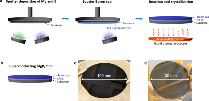
The overall flow of our MgB2 thin-film fabrication process utilizing magnetron sputtering is illustrated in Figure 1a, and the resulting superconducting MgB2 thin films on silicon and sapphire wafers are shown in Figure 1b,c, respectively. Magnetron sputtering is widely available, easily scalable, and produces uniform films, but in situ sputtered MgB2 films resulted in low Tc(23,34) from oxidation, small grain size, and/or off-stoichiometry due to a high vapor pressure and low sticking coefficient of magnesium at elevated temperatures over 200 °C, as well as contamination. Postannealing of these films shows improvements in Tc but at the cost of roughness (>10 nm rms). Room-temperature deposition results in a uniform distribution of magnesium but requires a postannealing process. Annealing magnesium–boron composite film in vacuum resulted in evaporation of magnesium, rough surface, and transition temperature around 6 K. Magnesium evaporation is prevented by capping the composite film with a thin (tens of nm) layer of high melting temperature material such as tantalum or boron. Tantalum does not react with magnesium or boron at typical annealing temperatures below 800 °C but cracks above 700 °C and needs to be removed for easily measuring superconducting properties. Boron, a dielectric material with a high melting point of 2076 °C, serves as a better capping layer. Surface boron oxide has a low melting point of 450 °C and provides a crack-free, viscous capping layer.35 There are two potential byproducts between MgB2 and boron: MgB4 and MgB7. Both have slightly higher formation energies compared to MgB2,36 so their formation would be minimal and would not affect the measurement of superconducting properties even if a thin layer of the byproducts is formed, because they are dielectric materials unlike metallic MgB2. We have developed and demonstrated fabrication maturity in removing these capping layers for device development and optimization. In our work, we tried many deposition conditions, and mostly through optimizing the roughness of the film, we chose a codeposited Mg–B precursor film at room temperature. Sputtering of boron is very challenging, and a high melting point leads to a very low deposition rate. Given the propensity for oxidation, we optimized the boron sputtering for a maximum rate and then tuned the magnesium sputtering conditions and annealing process to achieve optimized films. In order to achieve smooth films, the as-deposited, preannealed Mg–B composite film must be as smooth as possible. A small amount of RF substrate bias (15 W) during deposition reduced the surface roughness from 1.74 nm to 0.34 to 0.476 nm (rms). Increasing the bias beyond this point gave denser films but etched Mg or heated the surface too much to achieve controllable stoichiometry in a cosputtered film. We saw indications that even this low substrate bias provided enough energy to induce some reaction between Mg and B as we started to see transitions in as-sputtered films before any postannealing step, though Tc,0 was below liquid helium temperatures.
Figure 1.
Schematic illustration of superconducting MgB2 thin-film fabrication process flow. (a) Left: magnesium and boron are cosputtered onto a rotating substrate to a desired thickness (e.g., 50 nm). A small substrate bias (e.g., 15 W) is applied to achieve a smooth surface. Center: a thin boron capping layer is deposited on top of the cosputtered film. Right: the wafer sample is annealed at around 600 °C in a 100% nitrogen environment for 2–10 min in a rapid thermal processor. (b) The final product is a superconducting thin MgB2 film with a boron cap on a substrate. (c) MgB2 thin film on a 100 mm diameter single-crystal silicon substrate with a thin (30 nm) silicon nitride buffer layer. (d) MgB2 thin film on a 100 mm diameter single-crystal sapphire substrate.
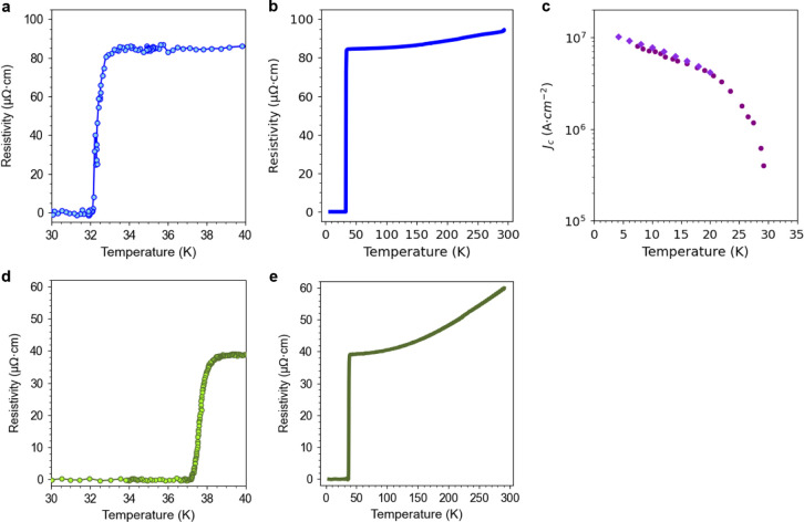
A rapid thermal processor (RTP) provides good thermal uniformity across large wafers and was used for postannealing. Because magnesium vapor pressure jumps around its melting point of 650 °C, it is critical to keep the annealing temperature below this temperature to avoid any potential surface roughening caused by evaporated magnesium that has yet to react with boron. By optimizing the annealing condition, we measured Tc,0 of 32 K (Figure 2a,b) for devices from MgB2 thin films with 0.476 nm rms roughness (Figure 3a) and a circular area of 100 mm diameter. We further achieved Tc,0 of 37.2 K, shown in Figure 2c,d, highest ever reported for sputtered film, by inducing large grains, thus sacrificing surface roughness, from postannealing interchanging magnesium and boron layers of stoichiometric ratio (2 boron to 1 magnesium atomic ratio), similar to previous attempts,37−41 but with an additional boron capping layer on top. The massive migration of magnesium into the interfacing boron layers led to large MgB2 grains and high Tc, but at the same time, it resulted in large voids and rough surfaces. Certain applications may take advantage of these films, particularly when devices have a very small active area.
Figure 2.
DC superconducting properties of MgB2 thin films. (a) Resistivity versus temperature plot of a MgB2 thin film showing superconducting transition with Tc,0 = 32 K and (b) shown across a wider temperature range from 4.2 to 300 K. (c) Critical current density (Jc) of two superconducting MgB2 thin films at different temperatures (Jc > 107 MA·cm–2 at 4.2 K) showing reproducibility of the films. (d) Resistivity versus temperature plot of MgB2 film with Tc,0 = 37.2 K, highest ever reported for sputtered MgB2 film, and (e) shown across a wider temperature range from 4.2 to 300 K.
Figure 3.
Morphological characterizations of postannealed MgB2 thin films. (a) Atomic force microscopy of the MgB2 thin film with Tc,0 of 32 K (Figure 2a) and the surface roughness of 0.476 nm rms. (b) High-angle annular dark-field (HAADF) STEM image of 40 nm thick superconducting MgB2 thin film with a 30 nm boron cap layer on a high-resistivity silicon wafer with a 30 nm silicon nitride buffer layer, showing sharp interfaces. (c) Deviation from the median magnesium to boron ratio in 40 nm thick boron-rich MgB2 film samples on the silicon nitride buffer layer (red) and sapphire (blue) analyzed by depth-profile X-ray photoelectron spectroscopy. The magnesium to boron ratio stays within 10% of the median for samples on silicon nitride. Significant migration of magnesium from the MgB2 layer to sapphire results in huge deviation of −30% from the median ratio near the interface. The range of deviation from the median Mg:B ratio for the sample on silicon nitride is shaded in gray.
Sapphire substrates have often been used for growing MgB2 films because both have hexagonal crystal structure and lattice mismatch is less than 0.1% with 30° rotation.42 However, oxygen readily diffuses from sapphire to MgB2 because magnesium has lower oxidation enthalpy compared to aluminum43 and forms an interdiffusion layer.18 This is especially detrimental for thin films under 100 nm. An alternative substrate is hexagonal SiC, especially for in situ growth of MgB2, because of the close lattice match. In fact, the highest Tc ever measured for MgB2 is from highly textured MgB2 thin film slightly strained by SiC.15 However, SiC is more expensive than Si, and polycrystalline MgB2 films from the postannealing process would not be able to take advantage of the lattice match. Because magnesium reacts with silicon to form Mg2Si, a thin inert buffer layer was used to prevent direct contact between MgB2 and Si. As was demonstrated previously,33 silicon nitride proved to be unreactive against magnesium, and LPCVD nitride as thin as 30 nm has been successfully tested to be sufficiently thick enough to serve as a good buffer, as shown in the STEM image in Figure 3b. In theory, the thickness is limited to only the threshold where no pinholes are left exposing Si, mostly dominated by the initial substrate roughness. The LPCVD nitride deposition on Si wafers is a highly commercialized process,44 not requiring the development of an independent recipe specific to MgB2 thin films. Early in our work, we found that identical deposition and annealing recipes resulted in a higher critical temperature on a silicon nitride buffer than on sapphire. Later, it was confirmed through X-ray photoelectron spectroscopy (XPS) that magnesium from the MgB2 layer migrated to the sapphire substrate and resulted in large deviation in stoichiometry of the film near film/substrate interface (Figure 3c).
MgB2 film uniformity
is confirmed by mapping sheet resistance
measurements by eddy current on insulating wafers, such as high-resistivity
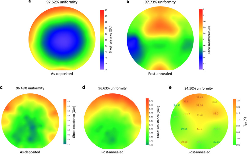
silicon or sapphire, as well as measuring Tc,0 at 15 different points across a wafer. As-deposited Mg–B
composite films and post-rapid-annealed MgB2 thin films
of two different thicknesses (50 and 100 nm as-deposited, reduced
by 20% to 40 and 80 nm postannealed) on 100 mm diameter wafers shown
in Figure 4a–d
demonstrate 1−σ wafer uniformities of sheet resistance
ranging between 96.49% and 97.73%. The nonuniformity of as-deposited
films is limited by the target size and geometric configuration of
the sputtering system and could be improved with larger targets. Postannealed
films’ sheet resistance distribution change comes from the
thermal gradient inside rapid thermal processors. The wafer uniformity
of Tc,0 for an 80 nm thick MgB2 film is 94.50%, as shown in Figure 4e. Here, the nonuniformity is calculated by  , as the number of sample
points is much
smaller than 30. It is difficult to directly correlate the distribution
of Tc,0 with the sheet resistances in Figure 4c,d, because regions
with slightly higher as-deposited sheet resistance imply slight magnesium
deficiency (thus resulting in lower Tc,0 given identical annealing conditions), while regions with higher
annealing temperatures inside RTP also exhibit higher sheet resistance
given identical magnesium content but with higher Tc,0. In general, the top part of the wafer experienced
slightly higher annealing temperature, resulting in higher Tc,0. The effect of magnesium deficiency is evident
in the top-left region of Figure 4e by two Tc,0 points, 30.35
and 32.8 K, of which the former had significant magnesium deficiency
evidenced from higher as-deposited sheet resistance in Figure 4c, while the latter had higher
magnesium content (lower as-deposited sheet resistance), confirming
that the film is in the dirty-limit with a short electron mean-free
path.45
Figure 4.
Eddy current maps of (a) 50 nm thick as-deposited Mg–B composite film with 85 W RF power on magnesium target, (b) 40 nm thick postannealed MgB2 film after annealing at 600 °C for 10 min, (c) 100 nm thick as-deposited Mg–B composite film with 95 W RF power on magnesium target, and (d) 80 nm thick postannealed MgB2 film after annealing at 585–590 °C for 2 min followed by 600–615 °C for 4 min. Sheet resistances from eddy current measurements directly correspond to magnesium (as-deposited) and MgB2 (postannealed) distributions. The sheet resistance wafer uniformities (% of wafer within 1−σ of the average sheet resistance) are between 96.49% and 97.73%. (e) Tc,0 distribution across the 100 mm diameter postannealed MgB2 film measured at 15 different points. The Tc,0 wafer uniformity is 94.50%, calculated by 1 – (Tc,0 max – Tc,0 min)/(2 × Tc,0 average) as the number of sample points is much smaller than 30.
DC superconducting properties of these films were investigated as a function of film thickness by etching back films using an argon ion mill. While this postprocessing is not an ideal method for achieving thin films, there is sufficient evidence to support that grain connectivity of as-grown thin films is poor.46 This also seems to impact polycrystalline films grown by MBE47 which exhibits thickness-dependent resistivity far beyond the thickness equivalent to the grain size in the films (10–20 nm). Resistivities of films with different thicknesses versus temperature are plotted in Figure 5. As expected, Tc,0 decreases as thickness decreases. The most etched back film with 6.9 ± 0.4 nm thickness showed Tc,0 of 21.4 K, higher than the reported value of 16 K for a 7.5 nm thick MgB2 film that was grown on sapphire by MBE, followed by rapid annealing without a boron capping layer.47 Normal state resistivity increases only slightly, and the absolute normal state resistivity values are also smaller than the films fabricated by coevaporation,48 implying good connectivity of MgB2 grains in our etched back films. The resistivities are larger than the ion-milled HPCVD films49 because the grains are much larger in the HPCVD films, but the ratios of normal state resistivities at different thicknesses are smaller, suggesting that the resistivities are mainly affected by surface scattering in our etched back films, and the connectivity of MgB2 grains is retained even for the 6.9 ± 0.4 nm thick film.
Figure 5.
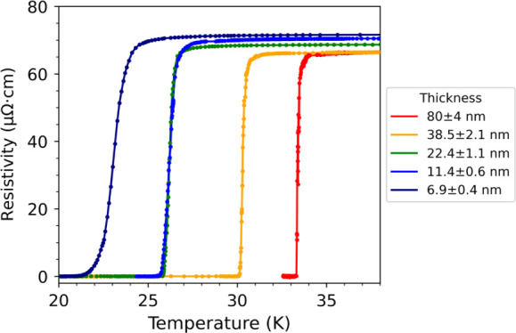
Resistivity versus temperature plots of MgB2 films of different thicknesses. The unetched 80 ± 4 nm thick film (red) has the highest superconducting transition temperature, Tc,0 = 33.3 K, followed by the film etched back to 38.5 ± 2.1 nm in thickness (orange) with Tc,0 = 30.1 K, followed by the film etched back to 22.4 ± 1.1 nm in thickness (green) with Tc,0 = 25.9 K, followed by the film etched back to 11.4 ± 0.6 nm in thickness (blue) with Tc,0 = 25.7 K, and followed by the film etched back to 6.9 ± 0.4 nm in thickness (navy) with Tc,0 = 21.4 K.
For device design and fabrication, controlling resistivity and related materials properties, such as kinetic inductance, brings a huge advantage. Typically, such a control is accomplished by deliberately adding impurities50 or changing stoichiometry.51 The high Tc MgB2 thin films therefore have a tremendous advantage when it comes to the range of resistivity/kinetic inductance control.31 Resistivity control in MgB2 can be performed by controlling the magnesium to boron ratios. Adding more boron or reducing the amount of magnesium by reducing the RF power on magnesium target increases the resistivity of as-deposited/preannealed Mg–B composite films gradually, as shown in Figure 6. Annealing the films causes magnesium particles to react with boron and form MgB2, resulting in a linear correlation between the resistivity of percolating magnesium (as-deposited) and percolating MgB2 (postannealed).
Figure 6.
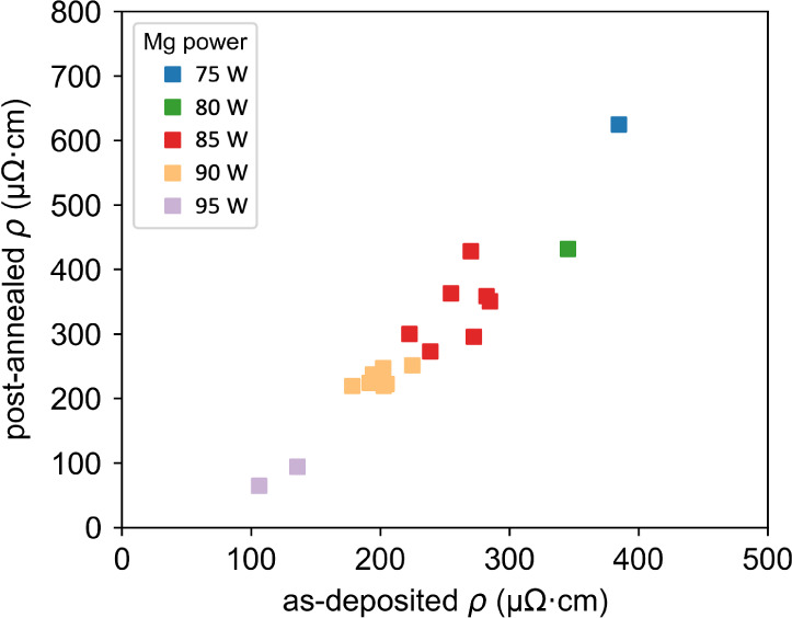
Postannealed resistivity of smooth (roughness <0.5 nm rms) MgB2 films (y axis) controlled by initial magnesium content in the as-deposited Mg–B composite films (resistivity along the x axis). Reducing the magnesium content (i.e., decreasing the relative RF power on the magnesium target) increases as-deposited resistivity as well as postannealed resistivity by forming boron-rich MgB2 films.
Superconducting Microdevices from Wafer-Scale MgB2 Films
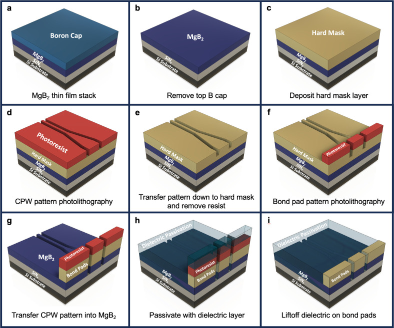
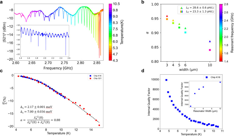
Here, we present and discuss results describing the internal quality factor and kinetic inductance of planar quarter-wave resonators patterned into our MgB2 thin films by using a coplanar waveguide (CPW) architecture. The overall flow of the device fabrication process is illustrated in Figure 7, fabricated wafer-scale devices are shown in Figure 8, and measurements and analyses of the devices are shown in Figure 9. We demonstrate fabrication maturity on par with more commonly used materials (e.g., NbTiN)52 and show figures of merit for microwave applications at higher temperatures. Given that the BCS surface resistance is both frequency- and temperature-dependent, better performance at lower frequencies and higher temperatures is a strong case for better performance at higher frequencies and lower temperatures. Work is ongoing to improve on dielectric losses in the film stack, as well as demonstrate high-frequency losses in the material, and will be published following those results. The losses in a superconducting resonator can be measured through the quality factor of the resonator. By fitting the resonator to a well-known model,53 we can obtain the internal microwave losses in the resonator. These losses include superconducting losses (from the BCS surface resistance), dielectric losses (in both the substrate/passivation layers and the interfaces), and radiative losses. While our initial goal of this experiment was to try to measure the BCS surface resistance in the films through troubleshooting and optimizing the losses, we have concluded that we are still dominated by dielectric losses in our thin film stack. By adopting standard fabrication techniques like a buffered oxide etch, we continue to see decreases in these losses, with Qi ∼ 104 at 4.5 K (Figure 9d). We assume that the losses are limited by dielectrics or interfaces for two reasons. First, as we cool to lower temperature, the value of Qi has no temperature dependence from 1.5 to 1 K, with the value about 4 × 10⁴. This saturation at a relatively high temperature is somewhat affected by the material’s high kinetic inductance, which strengthens the temperature dependence of the superconducting losses. Work is ongoing to measure these films below 1 K, which will help separate dielectric losses (specifically TLS) from quasi-particle losses. Another strong indicator that the losses in our devices are indeed limited by dielectrics (or interfaces) is that the quality factor is highly dependent on the width of the devices. Smaller devices have higher dielectric fill factors, and so the dielectric loss contribution goes up. The inset of Figure 9d shows the quality factor of 5 resonators (widths are 3, 4, 5, 6, and 10 um) of the same length (5 mm) scaling from ∼7500 to 10000. In the case that these losses are in the superconductor, there would be an f(2) dependence, and given that the widest traces yield the highest frequency resonators, they would have the lowest quality factors.
Figure 7.
Schematic illustration of a superconducting MgB2 coplanar waveguide device fabrication process flow.
Figure 8.
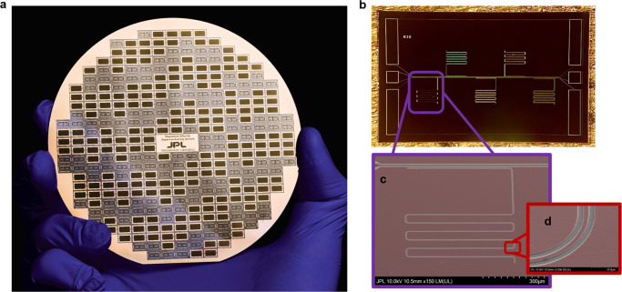
Wafer-scale MgB2 superconducting device demonstration. (a) Coplanar waveguide microwave resonators and other test chips patterned in MgB2 film deposited on a 100 mm sapphire substrate. (b) Optical image and (c, d) high-magnification SEM images (false color) for a resonator chip on the Si substrate. MgB2 film is denoted by the red area.
Figure 9.
MgB2 RF device measurements. (a) S21 transmission of a MgB2 resonator at different temperatures. Inset shows the five resonances corresponding to a perfect yield on this chip. (b) Alpha (α)—fraction of total inductance that originates from the superconducting kinetic inductance—for two different chips (plotted in triangles and squares) at different CPW conductor widths. The resonant frequency for each measurement is represented by the color fill. (c) Fractional frequency shift as a function of the temperature for two different resonator chips. Higher temperature data were not possible due to the high coupling factor to the resonators. In the future, we plan to design some low coupling resonators for better measurements up to the critical temperature. The fit is a crude two-gap model used by Yang et al.30 The gap values were highly constrained in the model to show the participation of the larger gap (about 12%) even for the polycrystalline films. (d) Internal quality factor (Qi) as a function of temperature. We performed interface cleaning processes to achieve Qi ≥ 104 and expect it to improve further as we mature the fabrication process. Inset shows the reduction in Qi seen for different cpw geometry (plotted as the center conductor width for Z0 = 50 ohms).
These resonators also serve to demonstrate the high kinetic
inductance
(Lk) prevalent in these films. Because
MgB2 does not have a typical temperature dependence, it
is not feasible to use the Mattis–Bardeen theory to estimate
α. Instead, one can compare the design frequency with the actual
frequency to accurately calculate the value of alpha,  , for the case
of α ≫ 0.25.54 Since the geometric
inductance and capacitance
do not change much with a different geometry of the same impedance,
we can easily see how the kinetic inductance fraction α changes
as a function of the width of the line. The design frequency of the
resonator was simulated to be close to 7 GHz, and the actual frequency
of the resonances falls between 1.5 and 2.8 GHz for conductor width
from 3 to 10 μm. In the same device used to describe the losses,
α goes from 0.84 at 10 μm line width to 0.95 at 3 μm
line width, with a consistent Lk = 22–24
pH/□. This is shown in Figure 9b where two chips from different wafers are shown.
In the second device, the same film recipe is used, but the films
are slightly thinner and so Lk = 28 pH/□.
The latter shows that even higher kinetic inductance can be readily
achieved. By tuning the Mg content in the precursor film, we can achieve
a range of 5–50 pH/□ for a similar film thickness (around
40 nm), since kinetic inductance is directly proportional to sheet
resistance.55 Using thinner films, we should
be able to achieve large kinetic inductance values on the order of
hundreds of pH/□. A systematic study of RF properties as a
function of the Mg content is ongoing. In these films, tuning the
stoichiometry is much more feasible than reactive gas sputtering during
which gas nonuniformity and hysteretic parameter curves become challenges
in depositing films such as NbN or TiN. We are also able to thin down
the films using an argon ion mill, or chlorine or bromine plasmas,56 without degradation of the superconducting properties
(within some limits). Argon ion milling has already been reported
for producing even thinner films than our etched back samples in Figure 5.49 Additionally, annealing a thicker film avoids surface tension,
requiring more energy to achieve the same grain size and hence achieving
higher critical temperature for thinned down films compared to annealing
thinner films of identical final thickness.
We have used a fairly simple model that assumes a linear combination of the penetration depths associated with the two gaps in the material30 to fit the temperature-dependent frequency shift of two different resonators. The high coupling quality factor (∼104) made it difficult to find the resonance above 10–15 K, and so the data do not go beyond this temperature; however, the fits shown in Figure 9c show that the contribution from the larger gap is small (∼12%), but non-negligible. This makes sense, given that the smaller gap is responsible for the bulk of the kinetic inductance, which is high in our films. Using our thin-film capability and expanding the two-gap model to include an interaction parameter that could also have temperature dependence, we hope to contribute to a global model for the contribution of the second gap to the overall film properties. Until now, film properties could not be reproduced under different conditions to modify the MB model for the two-gap material. Furthermore, there is only a rudimentary understanding on how these two gaps will affect high-frequency performance in the films,57 and how pairbreaking of the smaller gap will contribute to RF losses, while there still exists a larger gap. This is perhaps the most important future study planned for these films.
Conclusion
The ultrasmooth wafer-scale superconducting MgB2 films developed here can be readily used for nano- and microdevice fabrication, and by demonstrating key figures of merit, uniform and smooth large-scale film on the Si substrate with high Tc, Jc, and Lk, we have taken this technology to a level that can be immediately implemented. Historically, the low melting point and highly oxidizing nature of magnesium present multifold problems and have prevented any sustainable large-scale fabrication of MgB2 devices. We made uniform and smooth large-area as-deposited Mg–B composite films by RF sputtering and substrate biasing. The films were grown on the commercially available silicon substrate by adding a low-stress nitride buffer layer. By creating a closed environment with a boron capping layer (which forms several nanometers of viscous crack-free liquid oxide cap) and preventing magnesium evaporation during annealing, we were able to optimize the annealing temperature and time by a rapid thermal processor to achieve high Tc. We have further developed fabrication techniques for these films to achieve small critical features (0.5 μm demonstrated) and high yield. The devices demonstrate high Jc and low rf losses suitable for high-temperature/high-frequency superconducting photon detectors and transmission lines. The large nonlinear kinetic inductance shown in these films makes them a good candidate for high-frequency superconducting and quantum devices ranging from parametric amplifiers, frequency multipliers to kinetic inductance-based quantum computing qubits58 and circuits.
Methods
Precursor Mg–B composite, layered thin films, and boron caps were deposited by RF magnetron sputtering of 3″ elemental magnesium and boron targets at 1–2 mTorr and varying degrees of RF substrate biases. Magnesium sputtering power was varied between 50 and 250 W RF for different recipes, while boron sputtering power was fixed at 580 W RF. The silicon nitride buffer layer on the high-resistivity silicon substrate was deposited by Tystar LPCVD with 50–150 MPa tensile stress. Postannealing was done using SSI Solaris 150 Rapid Thermal Processor with a ramp rate of 1 °C per second for cosputtered films and 1–33 °C per second for layered films.
MgB2 devices are fabricated by first removing the boron cap with an argon ion mill. Because MgB2 decomposes and oxidizes when exposed to an oxidant (e.g., air and water), passivation throughout device fabrication processes is necessary. We developed a tripurpose titanium–gold bilayer, serving as an excellent passivation layer during fabrication (photolithography), a hardmask, and electrical contact pads after removal as a hardmask everywhere else on which a dielectric layer (silicon, silicon nitride, or aluminum nitride) is deposited for passivation. The devices are patterned by a Heidelberg maskless aligner (MLA 150) with AZ5209-E or OiR 620 photoresists. After developing, the titanium layer not covered by photoresist is etched with chlorine ICP (10 sccm of BCl3 and 35 sccm of Cl2 at 7 mTorr with 200–400 W ICP power and 30 W substrate bias power). Once the pattern is transferred onto the titanium layer, photoresist is removed with acetone, and then, the entire sample is ion-milled so that only the MgB2 device layer is left.
XPS depth profiling was done using Kratos Axis Ultra, with a base pressure of 1 × 10⁻⁹ Torr in the analysis chamber without etching or 5 × 10⁻⁸ Torr during etching. A monochromatic Al Kα X-ray source with a 1486.7 eV of energy at 150 W was used. Etching was done with an Ar+ ion beam with a 2 kV beam energy over a 2 × 2 mm2 area. All spectra were collected with a resolution of 0.1 eV, a pass energy of 20 eV, and a 110 μm spot size during etching. Spectra were charge-corrected to adventitious C at 284.8 eV. Spectra were fit by using CasaXPS software. All spectra used a Shirley background.
DC resistance and current density were measured using a four-point method. RF measurements were done in a liquid helium dewar on a custom dipstick using a vector network analyzer.
We prepared the TEM lamella using focused ion beam milling (Raith Velion) with gold (Au+) from a MgB2 sample that was deposited on a silicon wafer with a nitride buffer layer and postannealed at 600 °C for 2 min. Platinum was deposited on top of the film as part of lamella preparation. The lamella was heated in a vacuum oven at 150 °C overnight to minimize carbon contamination prior to imaging. The interfaces of the lamella were imaged in a 200 keV aberration-corrected STEM (Themis).
Acknowledgments
The research by C. Kim, C. Bell, J. Greenfield, and D. Cunnane was carried out at the Jet Propulsion Laboratory, California Institute of Technology, under a contract with the National Aeronautics and Space Administration (80NM0018D0004). This work was primarily supported by the Nancy Grace Roman Technology Fellowship in Astrophysics and NASA Research Opportunities in Space and Earth Sciences (NNH20ZDA001N-APRA). We acknowledge the support and infrastructure provided for this work by the Microdevices Laboratory at JPL and the Kavli Nanoscience Institute at Caltech. We thank H. LeDuc, B. Bumble, and A. Beyer for advice on device fabrication, P. Day for discussions and support on RF measurements, M. Dickie for chemical vapor deposition of silicon nitride buffer layer, and A. Wertheim for discussions on sputter depositions. The XPS was carried out at the Molecular Materials Resource Center in the Beckman Institute at the California Institute of Technology and supported by the U.S. Department of Energy grant numbers DE-SC0004993 and DE-SC0022087. The STEM work was completed in MIT.nano facilities. We thank Juan Ferrera for assistance in preparing the TEM lamella. E. Batson acknowledges the National Science Foundation Graduate Research Fellowship under Grant No. 2141064 and the NSF CQN program under Grant No. EEC1941583.
Supporting Information Available
The Supporting Information is available free of charge at https://pubs.acs.org/doi/10.1021/acsnano.4c11001.
Author Contributions
C.K. and D.P.C. conceived and designed the experimental protocol. C.K. prepared and optimized the films. C.K. performed eddy current, cryogenic DC conductivity, and AFM measurements. D.P.C. designed the resonator patterns. C.K. fabricated the devices. C.B., J.G., and D.P.C. performed cryogenic RF measurements. C.K. and D.P.C. interpreted the results. J.M.E. performed XPS depth-profiling and analyzed the data. N.S.L. secured funding for the XPS equipment and analysis. E.B. performed sampling and STEM imaging of the MgB2 lamella. K.K.B. supervised E.B.’s work. D.P.C. provided guidance throughout the project. C.K. and D.P.C. wrote the manuscript. All the coauthors discussed the results and helped revise the manuscript.
The authors declare the following competing financial interest(s): The California Institute of Technology has filed a U.S. utility patent with the title Wafer scale production of superconducting magnesium diboride thin films with high transition temperature (inventors: C.K. and D.P.C.) describing the superconducting magnesium diboride thin film and device fabrication methods described in this paper.
Notes
Kim, C.; Bell, C.; Evans, J.; Greenfield, J.; Batson, E.; Berggren, K.; Lewis, N.; Cunnane, D. Wafer-Scale MgB2 Superconducting Devices. 2023; arxiv.2305.15190, arXiv, https:// https://arxiv.org/abs/2305.15190, accessed August 21, 2024. This manuscript includes thickness dependence of DC superconducting properties (Figure and associated discussions), which is not available in the preprint versions.
Supplementary Material
References
- Ade P. A. R.; Ahmed Z.; Amiri M.; Barkats D.; Thakur R. B.; Bischoff C. A.; Beck D.; Bock J. J.; Boenish H.; Bullock E.; Buza V.; Cheshire J. R. IV; Connors J.; Cornelison J.; Crumrine M.; Cukierman A.; Denison E. V.; Dierickx M.; Duband L.; Eiben M.; Fatigoni S.; Filippini J. P.; Fliescher S.; Goeckner-Wald N.; Goldfinger D. C.; Grayson J.; Grimes P.; Hall G.; Halal G.; Halpern M.; Hand E.; Harrison S.; Henderson S.; Hildebrandt S. R.; Hilton G. C.; Hubmayr J.; Hui H.; Irwin K. D.; Kang J.; Karkare K. S.; Karpel E.; Kefeli S.; Kernasovskiy S. A.; Kovac J. M.; Kuo C. L.; Lau K.; Leitch E. M.; Lennox A.; Megerian K. G.; Minutolo L.; Moncelsi L.; Nakato Y.; Namikawa T.; Nguyen H. T.; O’Brient R.; Ogburn R. W. IV; Palladino S.; Prouve T.; Pryke C.; Racine B.; Reintsema C. D.; Richter S.; Schillaci A.; Schwarz R.; Schmitt B. L.; Sheehy C. D.; Soliman A.; Germaine T. St.; Steinbach B.; Sudiwala R. V.; Teply G. P.; Thompson K. L.; Tolan J. E.; Tucker C.; Turner A. D.; Umiltà C.; Vergès C.; Vieregg A. G.; Wandui A.; Weber A. C.; Wiebe D. V.; Willmert J.; Wong C. L.; Wu W. L. K.; Yang H.; Yoon K. W.; Young E.; Yu C.; Zeng L.; Zhang C.; Zhang S. BICEP/Keck XV: The BICEP3 Cosmic Microwave Background Polarimeter and the First Three-Year Data Set. Astrophys. J. 2022, 927 (1), 77. 10.3847/1538-4357/ac4886. [DOI] [Google Scholar]
- Day P. K.; LeDuc H. G.; Mazin B. A.; Vayonakis A.; Zmuidzinas J. A Broadband Superconducting Detector Suitable for Use in Large Arrays. Nature 2003, 425 (6960), 817–821. 10.1038/nature02037. [DOI] [PubMed] [Google Scholar]
- Echternach P. M.; Pepper B. J.; Reck T.; Bradford C. M. Single Photon Detection of 1.5 THz Radiation with the Quantum Capacitance Detector. Nat. Astron. 2018, 2 (1), 90–97. 10.1038/s41550-017-0294-y. [DOI] [Google Scholar]
- Mattioli F.; Zhou Z.; Gaggero A.; Gaudio R.; Jahanmirinejad S.; Sahin D.; Marsili F.; Leoni R.; Fiore A. Photon-Number-Resolving Superconducting Nanowire Detectors. Supercond. Sci. Technol. 2015, 28 (10), 104001. 10.1088/0953-2048/28/10/104001. [DOI] [Google Scholar]
- Zmuidzinas J.; Ugras N. G.; Miller D.; Gaidis M.; LeDuc H. G.; Stern J. A. Low-Noise Slot Antenna SIS Mixers. IEEE Trans. Appl. Supercond. 1995, 5 (2), 3053–3056. 10.1109/77.403236. [DOI] [Google Scholar]
- Cherednichenko S.; Drakinskiy V.; Berg T.; Khosropanah P.; Kollberg E. Hot-Electron Bolometer Terahertz Mixers for the Herschel Space Observatory. Rev. Sci. Instrum. 2008, 79 (3), 034501. 10.1063/1.2890099. [DOI] [PubMed] [Google Scholar]
- Macklin C.; O’Brien K.; Hover D.; Schwartz M. E.; Bolkhovsky V.; Zhang X.; Oliver W. D.; Siddiqi I. A near–Quantum-Limited Josephson Traveling-Wave Parametric Amplifier. Science 2015, 350 (6258), 307–310. 10.1126/science.aaa8525. [DOI] [PubMed] [Google Scholar]
- Eom B. H.; Day P. K.; LeDuc H. G.; Zmuidzinas J. A Wideband, Low-Noise Superconducting Amplifier with High Dynamic Range. Nat. Phys. 2012, 8 (8), 623–627. 10.1038/nphys2356. [DOI] [Google Scholar]
- Arute F.; Arya K.; Babbush R.; Bacon D.; Bardin J. C.; Barends R.; Biswas R.; Boixo S.; Brandao F. G. S. L.; Buell D. A.; Burkett B.; Chen Y.; Chen Z.; Chiaro B.; Collins R.; Courtney W.; Dunsworth A.; Farhi E.; Foxen B.; Fowler A.; Gidney C.; Giustina M.; Graff R.; Guerin K.; Habegger S.; Harrigan M. P.; Hartmann M. J.; Ho A.; Hoffmann M.; Huang T.; Humble T. S.; Isakov S. V.; Jeffrey E.; Jiang Z.; Kafri D.; Kechedzhi K.; Kelly J.; Klimov P. V.; Knysh S.; Korotkov A.; Kostritsa F.; Landhuis D.; Lindmark M.; Lucero E.; Lyakh D.; Mandrà S.; McClean J. R.; McEwen M.; Megrant A.; Mi X.; Michielsen K.; Mohseni M.; Mutus J.; Naaman O.; Neeley M.; Neill C.; Niu M. Y.; Ostby E.; Petukhov A.; Platt J. C.; Quintana C.; Rieffel E. G.; Roushan P.; Rubin N. C.; Sank D.; Satzinger K. J.; Smelyanskiy V.; Sung K. J.; Trevithick M. D.; Vainsencher A.; Villalonga B.; White T.; Yao Z. J.; Yeh P.; Zalcman A.; Neven H.; Martinis J. M. Quantum Supremacy Using a Programmable Superconducting Processor. Nature 2019, 574 (7779), 505–510. 10.1038/s41586-019-1666-5. [DOI] [PubMed] [Google Scholar]
- Hubmayr J.; Beall J.; Becker D.; Cho H.-M.; Devlin M.; Dober B.; Groppi C.; Hilton G. C.; Irwin K. D.; Li D.; Mauskopf P.; Pappas D. P.; Van Lanen J.; Vissers M. R.; Wang Y.; Wei L. F.; Gao J. Photon-Noise Limited Sensitivity in Titanium Nitride Kinetic Inductance Detectors. Appl. Phys. Lett. 2015, 106 (7), 073505. 10.1063/1.4913418. [DOI] [Google Scholar]
- Bretz-Sullivan T. M.; Lewis R. M.; Lima-Sharma A. L.; Lidsky D.; Smyth C. M.; Harris C. T.; Venuti M.; Eley S.; Lu T.-M. High Kinetic Inductance NbTiN Superconducting Transmission Line Resonators in the Very Thin Film Limit. Appl. Phys. Lett. 2022, 121 (5), 052602. 10.1063/5.0100961. [DOI] [Google Scholar]
- Jones G.; Johnson B. R.; Abitbol M. H.; Ade P. A. R.; Bryan S.; Cho H.-M.; Day P.; Flanigan D.; Irwin K. D.; Li D.; Mauskopf P.; McCarrick H.; Miller A.; Song Y. R.; Tucker C. High Quality Factor Manganese-Doped Aluminum Lumped-Element Kinetic Inductance Detectors Sensitive to Frequencies below 100 GHz. Appl. Phys. Lett. 2017, 110 (22), 222601. 10.1063/1.4984105. [DOI] [Google Scholar]
- Grünhaupt L.; Maleeva N.; Skacel S. T.; Calvo M.; Levy-Bertrand F.; Ustinov A. V.; Rotzinger H.; Monfardini A.; Catelani G.; Pop I. M. Loss Mechanisms and Quasiparticle Dynamics in Superconducting Microwave Resonators Made of Thin-Film Granular Aluminum. Phys. Rev. Lett. 2018, 121 (11), 117001. 10.1103/PhysRevLett.121.117001. [DOI] [PubMed] [Google Scholar]
- Nagamatsu J.; Nakagawa N.; Muranaka T.; Zenitani Y.; Akimitsu J. Superconductivity at 39 K in Magnesium Diboride. Nature 2001, 410 (6824), 63–64. 10.1038/35065039. [DOI] [PubMed] [Google Scholar]
- Xi X. X.; Pogrebnyakov A. V.; Xu S. Y.; Chen K.; Cui Y.; Maertz E. C.; Zhuang C. G.; Li Q.; Lamborn D. R.; Redwing J. M.; Liu Z. K.; Soukiassian A.; Schlom D. G.; Weng X. J.; Dickey E. C.; Chen Y. B.; Tian W.; Pan X. Q.; Cybart S. A.; Dynes R. C. MgB2 Thin Films by Hybrid Physical–Chemical Vapor Deposition. Phys. C 2007, 456 (1–2), 22–37. 10.1016/j.physc.2007.01.029. [DOI] [Google Scholar]
- Brinkman A.; Golubov A. A.; Rogalla H.; Dolgov O. V.; Kortus J.; Kong Y.; Jepsen O.; Andersen O. K. Multiband Model for Tunneling in MgB2 Junctions. Phys. Rev. B 2002, 65 (18), 180517. 10.1103/PhysRevB.65.180517. [DOI] [Google Scholar]
- Eskildsen M. R.; Kugler M.; Levy G.; Tanaka S.; Jun J.; Kazakov S. M.; Karpinski J.; Fischer Ø. Scanning Tunneling Spectroscopy on Single Crystal MgB2. Phys. C 2003, 385 (1–2), 169–176. 10.1016/S0921-4534(02)02301-8. [DOI] [Google Scholar]
- Zeng X.; Pogrebnyakov A. V.; Kotcharov A.; Jones J. E.; Xi X. X.; Lysczek E. M.; Redwing J. M.; Xu S.; Li Q.; Lettieri J.; Schlom D. G.; Tian W.; Pan X.; Liu Z.-K. In Situ Epitaxial MgB2 Thin Films for Superconducting Electronics. Nat. Mater. 2002, 1 (1), 35–38. 10.1038/nmat703. [DOI] [PubMed] [Google Scholar]
- Liu Z.-K.; Schlom D. G.; Li Q.; Xi X. X. Thermodynamics of the Mg–B System: Implications for the Deposition of MgB2 Thin Films. Appl. Phys. Lett. 2001, 78 (23), 3678–3680. 10.1063/1.1376145. [DOI] [Google Scholar]
- Kim J.; Singh R. K.; Newman N.; Rowell J. M. Thermochemistry of MgB2 Thin Film Synthesis. IEEE Trans. Appl. Supercond. 2003, 13 (2), 3238–3241. 10.1109/TASC.2003.812210. [DOI] [Google Scholar]
- Kang W. N.; Kim H.-J.; Choi E.-M.; Jung C. U.; Lee S.-I. MgB 2 Superconducting Thin Films with a Transition Temperature of 39 Kelvin. Science 2001, 292 (5521), 1521–1523. 10.1126/science.1060822. [DOI] [PubMed] [Google Scholar]
- Saito A.; Kawakami A.; Shimakage H.; Wang Z. As-Grown Deposition of Superconducting MgB2 Thin Films by Multiple-Target Sputtering System. Jpn. J. Appl. Phys. 2002, 41 (2A), L127. 10.1143/JJAP.41.L127. [DOI] [Google Scholar]
- Schneider R.; Geerk J.; Linker G.; Ratzel F.; Zaitsev A. G.; Obst B. In Situ Deposition of MgB2 Thin Films by Magnetron Cosputtering and Sputtering Combined with Thermal Evaporation. Phys. C 2005, 423 (3–4), 89–95. 10.1016/j.physc.2005.04.004. [DOI] [Google Scholar]
- Naito M.; Ueda K. MgB2 Thin Films for Superconducting Electronics. Supercond. Sci. Technol. 2004, 17 (7), R1–R18. 10.1088/0953-2048/17/7/R01. [DOI] [Google Scholar]
- Mijatovic D.; Brinkman A.; Oomen I.; Rijnders G.; Hilgenkamp H.; Rogalla H.; Blank D. H. A. Magnesium-Diboride Ramp-Type Josephson Junctions. Appl. Phys. Lett. 2002, 80 (12), 2141–2143. 10.1063/1.1462869. [DOI] [Google Scholar]
- Brinkman A.; Rowell J. M. MgB2 Tunnel Junctions and SQUIDs. Phys. C 2007, 456 (1), 188–195. 10.1016/j.physc.2007.01.019. [DOI] [Google Scholar]
- Yoshioka N.; Yagi I.; Shishido H.; Yotsuya T.; Miyajima S.; Fujimaki A.; Miki S.; Wang Z.; Ishida T. Current-Biased Kinetic Inductance Detector Using MgB2 Nanowires for Detecting Neutrons. IEEE Trans. Appl. Supercond. 2013, 23 (3), 2400604. 10.1109/TASC.2013.2243812. [DOI] [Google Scholar]
- Cunnane D.; Kawamura J. H.; Acharya N.; Wolak M. A.; Xi X. X.; Karasik B. S. Low-Noise THz MgB2 Josephson Mixer. Appl. Phys. Lett. 2016, 109 (11), 112602. 10.1063/1.4962634. [DOI] [Google Scholar]
- Novoselov E.; Cherednichenko S. Low Noise Terahertz MgB2 Hot-Electron Bolometer Mixers with an 11 GHz Bandwidth. Appl. Phys. Lett. 2017, 110 (3), 032601. 10.1063/1.4974312. [DOI] [Google Scholar]
- Yang C.; Niu R. R.; Guo Z. S.; Cai X. W.; Chu H. M.; Yang K.; Wang Y.; Feng Q. R.; Gan Z. Z. Lumped Element Kinetic Inductance Detectors Based on Two-Gap MgB2 Thin Films. Appl. Phys. Lett. 2018, 112 (2), 022601. 10.1063/1.5013286. [DOI] [Google Scholar]
- Cherednichenko S.; Acharya N.; Novoselov E.; Drakinskiy V. Low Kinetic Inductance Superconducting MgB2 Nanowires with a 130 Ps Relaxation Time for Single-Photon Detection Applications. Supercond. Sci. Technol. 2021, 34 (4), 044001. 10.1088/1361-6668/abdeda. [DOI] [Google Scholar]
- Gan Y.; Mirzaei B.; Silva J. R. G. D.; Chang J.; Cherednichenko S.; Van Der Tak F.; Gao J. R. Low Noise MgB2 Hot Electron Bolometer Mixer Operated at 5.3 THz and at 20 K. Appl. Phys. Lett. 2021, 119 (20), 202601. 10.1063/5.0070153. [DOI] [Google Scholar]
- Moeckly B. H.; Ruby W. S. Growth of High-Quality Large-Area MgB2 Thin Films by Reactive Evaporation. Supercond. Sci. Technol. 2006, 19 (6), L21–L24. 10.1088/0953-2048/19/6/L02. [DOI] [Google Scholar]
- Shimakage H.; Miki S.; Tsujimoto K.; Wang Z.; Ishida T.; Tonouchi M. Characteristics of As-Grown MgB2 Thin Films Made by Sputtering. IEEE Trans. Appl. Supercond. 2005, 15 (2), 3269–3272. 10.1109/TASC.2005.848849. [DOI] [Google Scholar]
- Napolitano A.; Macedo P. B.; Hawkins E. G. Viscosity and Density of Boron Trioxide. J. Am. Ceram. Soc. 1965, 48 (12), 613–616. 10.1111/j.1151-2916.1965.tb14690.x. [DOI] [Google Scholar]
- Balducci G.; Brutti S.; Ciccioli A.; Gigli G.; Manfrinetti P.; Palenzona A.; Butman M. F.; Kudin L. Thermodynamics of the Intermediate Phases in the Mg–B System. J. Phys. Chem. Solids 2005, 66 (2–4), 292–297. 10.1016/j.jpcs.2004.06.063. [DOI] [Google Scholar]
- Zhu H. M.; Zhang Y. B.; Sun X. L.; Xiong W. J.; Zhou S. P. MgB2 Thin Films on Si(111) without a Buffer Layer Prepared by e-Beam Evaporation. Phys. C 2007, 452 (1–2), 11–15. 10.1016/j.physc.2006.11.009. [DOI] [Google Scholar]
- Dai Q.; Kong X.; Feng Q.; Yang Q.; Zhang H.; Nie R.; Han L.; Ma Y.; Wang F. MgB2 Films Prepared by Rapid Annealing Method. Phys. C 2012, 475, 24–27. 10.1016/j.physc.2012.01.014. [DOI] [Google Scholar]
- Chromik Š.; Nishida A.; Štrbík V.; Gregor M.; Espinós J. P.; Liday J.; Durný R. The Distribution of Elements in Sequentially Prepared MgB2 on SiC Buffered Si Substrate and Possible Pinning Mechanisms. Appl. Surf. Sci. 2013, 269, 29–32. 10.1016/j.apsusc.2012.10.019. [DOI] [Google Scholar]
- Altin E.; Kurt F.; Altin S.; Yakinci M. E.; Yakinci Z. D. MgB2 Thin Film Fabrication with Excess Mg by Sequential e-Beam Evaporation and Transport Properties under Magnetic Fields. Curr. Appl. Phys. 2014, 14 (3), 245–250. 10.1016/j.cap.2013.11.023. [DOI] [Google Scholar]
- Beckham J. L.; Bayu Aji L. B.; Baker A. A.; Bae J. H.; Stavrou E.; Jacob R. E.; McCall S. K.; Kucheyev S. O. Superconducting Films of MgB2 via Ion Beam Mixing of Mg/B Multilayers. J. Phys. D: Appl. Phys. 2020, 53 (20), 205302. 10.1088/1361-6463/ab7624. [DOI] [Google Scholar]
- Seong W. K.; Oh S.; Kang W. N. Perfect Domain-Lattice Matching between MgB2 and Al2O3: Single-Crystal MgB2 Thin Films Grown on Sapphire. Jpn. J. Appl. Phys. 2012, 51, 083101. 10.1143/JJAP.51.083101. [DOI] [Google Scholar]
- Hasegawa M.Chapter 3.3 - Ellingham Diagram. In Treatise on Process Metallurgy, Seetharaman S., Ed.; Elsevier: Boston, MA, 2014; pp. 507–516.. DOI: 10.1016/B978-0-08-096986-2.00032-1. [DOI] [Google Scholar]
- Roenigk K. F.; Jensen K. F. Low Pressure CVD of Silicon Nitride. J. Electrochem. Soc. 1987, 134, 1777–1785. 10.1149/1.2100756. [DOI] [Google Scholar]
- Rowell J. M. The Widely Variable Resistivity of MgB2 Samples. Supercond. Sci. Technol. 2003, 16 (6), R17–R27. 10.1088/0953-2048/16/6/201. [DOI] [Google Scholar]
- Zhang Y.; Lin Z.; Dai Q.; Li D.; Wang Y.; Zhang Y.; Wang Y.; Feng Q. Ultrathin MgB2 Films Fabricated on Al2O3 Substrate by Hybrid Physical–Chemical Vapor Deposition with High Tc and Jc. Supercond. Sci. Technol. 2011, 24 (1), 015013. 10.1088/0953-2048/24/1/015013. [DOI] [Google Scholar]
- Shibata H.; Akazaki T.; Tokura Y. Ultrathin MgB 2 Films Fabricated by Molecular Beam Epitaxy and Rapid Annealing. Supercond. Sci. Technol. 2013, 26 (3), 035005. 10.1088/0953-2048/26/3/035005. [DOI] [Google Scholar]
- Shimakage H.; Tatsumi M.; Wang Z. Ultrathin MgB2 Films Fabricated by the Co-Evaporation Method at High Mg Evaporation Rates. Supercond. Sci. Technol. 2008, 21 (9), 095009. 10.1088/0953-2048/21/9/095009. [DOI] [Google Scholar]
- Acharya N.; Wolak M. A.; Tan T.; Lee N.; Lang A. C.; Taheri M.; Cunnane D.; Karasik B. S.; Xi X. X. MgB2 Ultrathin Films Fabricated by Hybrid Physical Chemical Vapor Deposition and Ion Milling. APL Mater. 2016, 4 (8), 086114. 10.1063/1.4961635. [DOI] [Google Scholar]
- Ruggiero S. T.; Williams A.; Rippard W. H.; Clark A. M.; Deiker S. W.; Young B. A.; Vale L. R.; Ullom J. N. Dilute Al–Mn Alloys for Superconductor Device Applications. Nucl. Instrum. Methods Phys. Res., Sect. A 2004, 520 (1), 274–276. 10.1016/j.nima.2003.11.236. [DOI] [Google Scholar]
- Yemane Y. T.; Sowa M. J.; Zhang J.; Ju L.; Deguns E. W.; Strandwitz N. C.; Prinz F. B.; Provine J. Superconducting Niobium Titanium Nitride Thin Films Deposited by Plasma-Enhanced Atomic Layer Deposition. Supercond. Sci. Technol. 2017, 30 (9), 095010. 10.1088/1361-6668/aa7ce3. [DOI] [Google Scholar]
- Malnou M.; Vissers M. R.; Wheeler J. D.; Aumentado J.; Hubmayr J.; Ullom J. N.; Gao J. Three-Wave Mixing Kinetic Inductance Traveling-Wave Amplifier with Near-Quantum-Limited Noise Performance. PRX Quantum 2021, 2 (1), 010302. 10.1103/PRXQuantum.2.010302. [DOI] [Google Scholar]
- Carter F. W.; Khaire T. S.; Novosad V.; Chang C. L. Scraps: An Open-Source Python-Based Analysis Package for Analyzing and Plotting Superconducting Resonator Data. IEEE Trans. Appl. Supercond. 2017, 27 (4), 1–5. 10.1109/TASC.2016.2625767. [DOI] [Google Scholar]
- Gao J.The Physics of Superconducting Microwave Resonators; California Institute of Technology: Pasadena, CA, 2008. [Google Scholar]
- Annunziata A. J.; Santavicca D. F.; Frunzio L.; Catelani G.; Rooks M. J.; Frydman A.; Prober D. E. Tunable Superconducting Nanoinductors. Nanotechnology 2010, 21 (44), 445202. 10.1088/0957-4484/21/44/445202. [DOI] [PubMed] [Google Scholar]
- Shibata H. Fabrication of a MgB2 Nanowire Single-Photon Detector Using Br2–N2 Dry Etching. Appl. Phys. Express 2014, 7 (10), 103101. 10.7567/APEX.7.103101. [DOI] [Google Scholar]
- Gan Y.; Mirzaei B.; Silva J. R. G.; Cherednichenko S.; Van Der Tak F.; Gao J. R. Heterodyne Performance and Characteristics of Terahertz MgB2 Hot Electron Bolometers. J. Appl. Phys. 2023, 133 (7), 074503. 10.1063/5.0128791. [DOI] [Google Scholar]
- Faramarzi F.; Day P.; Glasby J.; Sypkens S.; Colangelo M.; Chamberlin R.; Mirhosseini M.; Schmidt K.; Berggren K. K.; Mauskopf P. Initial Design of a W-Band Superconducting Kinetic Inductance Qubit. IEEE Trans. Appl. Supercond. 2021, 31 (5), 1–5. 10.1109/TASC.2021.3065304. [DOI] [Google Scholar]
Associated Data
This section collects any data citations, data availability statements, or supplementary materials included in this article.


