

Abstract
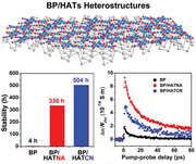
Overcoming the intrinsic instability and preserving unique electronic properties are key challenges for the practical applications of black phosphorus (BP) under ambient conditions. Here, it is demonstrated that molecular heterostructures of BP and hexaazatriphenylene derivatives (BP/HATs) enable improved environmental stability and charge transport properties. The strong interfacial coupling and charge transfer between the HATs and the BP lattice decrease the surface electron density and protect BP sheets from oxidation, resulting in an excellent ambient lifetime of up to 21 d. Importantly, HATs increase the charge scattering time of BP, contributing to an improved carrier mobility of 97 cm2 V‐1 s‐1, almost three times of the pristine BP films, based on noninvasive THz spectroscopic studies. The film mobility is an order of magnitude larger than previously reported values in exfoliated 2D materials. The strategy opens up new avenues for versatile applications of BP sheets and provides an effective method for tuning the physicochemical properties of other air‐sensitive 2D semiconductors.
Keywords: 2D materials, ambient stability, black phosphorus, charge carrier mobility, molecular heterostructures
A molecular engineering strategy is demonstrated to prepare ambient stable black phosphorus (BP)/hexaazatriphenylene (HAT) hybrid heterostructures. This strategy not only modifies the band structure of BP sheets but also improves their charge mobility, paving the way toward ambient processing and fabrication of high‐performance BP‐based devices.
1. Introduction
Black phosphorus (BP) is an attractive layered semiconductor thanks to its extraordinary band structure and puckered crystal lattice. It exhibits thickness‐dependent direct band gaps spanning from 0.3 to 2.0 eV,[ 1 , 2 ] a high charge carrier mobility of up to 1000 cm2 V‐1 s‐1,[ 3 ] and a remarkable current on/off ratio (≈104–105) as well as anisotropic thermal and electronic properties,[ 4 ] which are fascinating features for exploring next‐generation (opto)electronic devices.[ 5 , 6 ] Although BP is the most thermodynamically stable phosphorus allotrope, it is highly vulnerable to oxygen, moisture, and even light irradiation, due to abundant lone pair electrons at the BP surface.[ 7 , 8 ] In particular, the oxidative degradation of the exfoliated single‐ or few‐layer BP sheets completes within a few hours under ambient conditions, giving rise to rapid functional failure. Therefore, improving the environmental stability and modulating the physical properties of BP sheets are crucial criteria to fulfill their practical applications.
So far, various physical and chemical protocols have been implemented to protect the BP sheets from oxidation. For example, passivation of the BP surface with a thin layer of metal oxides (such as AlO x , TiO2)[ 9 , 10 ] or encapsulation with 2D materials (such as graphene, boron nitride)[ 11 , 12 ] is usually employed for the device physics studies. However, the fabrication of such inorganic heterostructures requires careful control of film quality or a tedious single‐sheet stacking process, limiting their scaled‐up practice. Alternatively, chemical functionalization is a preferred strategy in terms of using BP sheets toward solution processing and the precise control over the designed properties. For instance, covalent functionalization of BP, relying on the formation of P—C, P—O—C or P=N bonds with reactive intermediates such as free radicals,[ 13 ] nitrenes,[ 14 ] and carbocations,[ 15 ] protects the topological structure of BP sheets. However, this strategy largely compromises their electronic properties due to the direct breaking of P—P bonds. In contrast, non‐covalent functionalization (or surface coordination) using 1,2‐benzenedithiol on BP/Al3+,[ 16 ] Group 13 Lewis acids[ 17 ] (i.e., AlCl3 and AlBr3) or Pd–Pd units[ 18 ] can preserve or modify the intrinsic properties of BP sheets to a large extent. However, it is generally less effective to regulate electronic properties of BP because of the weak interfacial coupling.
Herein, we demonstrate an organic–inorganic hybrid heterostructure to enhance the stability of exfoliated few‐layer BP sheets and to tune simultaneously their electronic properties using hexaazatriphenylene derivatives (HATs). HATs have a high affinity to the lone pair electrons of P atoms. The decreased surface electron density and the molecularly thin coating layer impede the oxidation process of BP sheets and result in enhanced ambient stability up to 21 d (compared to only 4 h for pristine BP). Moreover, the strong charge transfer from BP sheets to electron‐acceptor moieties of HATs establishes a “built‐in” electric field at the interfaces, thus influencing the band gaps of BP sheets. The optical band gap (E g) and the valence band edge (E v) of BP/HATs molecular heterostructures are both tunable, depending on the HATs concentration. As HATs can increase the charge scattering time and expand the lifetime of free charge carriers in BP, the charge carrier mobility of BP/HATs thin films was substantially improved by three times to 97 cm2 V‐1 s‐1, disclosed by the THz spectroscopic investigations. This molecular engineering approach paves the way toward ambient processing and fabrication of high‐performance BP‐based devices.
2. Results and Discussion
We have designed two prototypes of hexaazatriphenylene derivatives (HATs), namely, 5,6,11,12,17,18‐hexaazatrinaphthylene (HATNA) and 1,4,5,8,9,11‐hexaazatriphenylenehexacarbonitrile (HATCN). Both molecules have planar structures and they contain an aromatic center and abundant cyano groups (with —C≡N or —C=N— bonds) that strongly interact with the BP surfaces through van der Waals force and π–π interaction, respectively. They also exhibit low lowest unoccupied molecular orbital (LUMO), strong electron affinity, unique charge transport properties[ 19 ] and good solubility in common organic solvents. For example, HATNA and HATCN exhibit LUMO levels of ‐6.6, ‐9.0 eV,[ 20 , 21 ] and electron affinity of 2.8, 4.9 eV,[ 22 , 23 ] respectively. All of these features make them easy to organize into atomically thin layers on the surfaces of the dispersed BP sheets, resulting in solution‐processable BP/HAT molecular heterostructures.
The HATs were synthesized according to the reported procedures,[ 24 ] and defect‐free BP nanosheets (3–10 layers) were prepared by an electrochemical exfoliation approach (Figure 1 and Figure S1, Supporting Information).[ 25 , 26 , 27 , 28 ] The noncovalent stacking process was performed in an argon‐filled glovebox. In a typical experiment, 0.1 mg of HATs was added into a 10 mL BP dispersion in dimethylformamide (DMF, 0.5 mg mL‐1). Then, the solution was gently stirred in the glovebox, resulting in a dark colloidal suspension after 24 h.
Figure 1.

Schematic illustration of the fabrication of BP/HAT molecular heterostructures in solutions.
The morphology and structure of the obtained BP and BP/HATs sheets were examined by scanning electron microscopy (SEM), transmission electron microscopy (TEM), and atomic force macroscopy (AFM). The BP/HATs sheets display a similar 2D nanostructure to the pristine BP sheets (Figures S2 and S3, Supporting Information), suggesting a negligible morphological change after the functionalization by HATs. By contrast, the average thickness of BP/HATNA and BP/HATCN changes to 5.2 and 5.5 nm, respectively, almost 1 nm thicker than the pristine exfoliated BP sheets (4.4 nm) based on a statistical calculation of more than 50 flakes from their AFM images (Figure 2a –c and Figure S4, Supporting Information). This result confirms the molecularly thin HAT layers on the BP surface. In addition, X‐ray diffraction (XRD) patterns of BP/HATs exhibit the same characteristic diffraction peaks as the pristine BP sheets (Figure 2g), indicating a well‐preserved lattice structure of BP. The elemental maps reveal that the P, C, and N are distributed homogeneously in BP/HATs films (Figures S5 and S6, Supporting Information), confirming the anchoring of the organic molecules onto the BP surface successfully. This result was also supported by blurred diffraction rings originating from the amorphous organic molecules and sharp diffraction spots from the BP lattice in selected area electron diffraction (SAED) patterns (Figure 2d–f). Moreover, high‐resolution TEM images (HR‐TEM) of BP/HATs do not present atomic fringes, which is consistent with the amorphous nature of HAT molecules (Figure S7, Supporting Information). The surface chemical composition of BP and BP/HATs sheets was elucidated by X‐ray photoelectron spectroscopy (XPS). As depicted in Figure 2h and Figure S8 (Supporting Information), the P 2p3/2 and P 2p1/2 peaks of pristine BP are located at 129.9 and 130.7 eV, respectively, in good agreement with the previous reports.[ 29 , 30 ] As for BP/HATs, new components (i.e., P+) centered at 129.6 and 130.4 eV are assigned to the positively charged P atoms.[ 31 ] Moreover, the N 1s spectra show a similar trend to P 2p (Figure 2i). Three components, namely, N‐ (397.7 eV), N0 (399.2 eV), and Ns (401.7 eV) in the N 1s spectra of BP/HATs, can be ascribed to the negatively charged molecules, electroneutral molecules, and the shakeup process,[ 32 , 33 ] respectively. The emerging P+ and N‐ species in both samples clearly indicate the electron transfer from P atoms into HATs molecules, leading to an electron accumulation layer in HATs and a depletion layer in BP, thus creating a “built‐in” electric field at BP/HATs interfaces (Figure S9, Supporting Information). Due to the higher electron affinity and lower LUMO of HATCN than HATNA, BP/HATCN possesses more pronounced P+ and N‐ peaks than BP/HATNA, causing a stronger electron transfer from BP to HATCN to form a stronger static electric field. This phenomenon was further supported by density functional theory (DFT) calculations.[ 34 , 35 ] Figure 2j,k and Figure S10 (Supporting Information) show an optimized adsorption configuration of the molecules on the BP surface. The adsorption energies of HATNA and HATCN on BP are 2.17 and 2.56 eV, respectively. Evidently, the higher adsorption energy of HATCN leads to the stronger interaction with BP than that of HATNA. The regions of electron accumulation and depletion are displayed in yellow and green, respectively. The charge distributions clearly show that strong electron accumulation occurs around the molecules, while hole accumulation appears at the BP surface (Figure S11, Supporting Information). This observation further proves that the adsorbed molecules can draw electrons from BP, thereby achieving p‐type doping. The average number of electrons transferred from a layer of BP to a HATNA or HATCN molecule is calculated to be 0.35 e or 0.65 e, respectively, which is consistent with the XPS results.
Figure 2.

Characterizations of BP and BP/HAT sheets. a–c) AFM images, d–f) SAED patterns, g) XRD patterns and h,i) high‐resolution XPS spectra of P 2p and N 1s of BP, BP/HATNA and BP/HATCN, respectively. j,k) The calculated charge densities of BP/HATNA (top) and BP/HATCN (bottom), respectively.
As a result, BP/HATs exhibit enhanced ambient stability compared with pristine BP. For example, in Figure 3a , the surface of BP sheets presents a dramatic change in a few hours. The emergence of P x O y in 4 h, in the form of small bubbles, evolves quickly to large particles within 12 h, similar with the previous reports.[ 17 ] Raman spectra confirm such a degradation process. As shown in Figure S12 (Supporting Information), BP has three characteristic modes,[ 36 , 37 ] namely, Ag 1, B2g, and Ag 2. The intensity ratio of Ag 1/Ag 2 is related to the oxidation levels.[ 38 ] Figure 3d reveals that the Ag 1/Ag 2 values of BP drop sharply to 0.08 after 12 h exposure, indicating severe oxidation. In contrast, BP/HATs are more stable under ambient conditions. As shown in Figure 3b,c, the morphology of BP/HATCN (5 nm thick) does not change after exposure in air for 14 d, some flakes around 10 nm thick are stable even after 21 d (Figure S13, Table S3, Supporting Information). Moreover, the ratios of Ag 1/Ag 2 in BP/HATs distribute in the range of 0.3–0.7, revealing good structural stability (Figure 3e,f). It is well known that the reactivity of BP is directly related to the lone electrons pairs of P atom.[ 17 ] In our approach, HATs could decrease surface electron density and organize into an encapsulating thin layer, preventing the access of oxygen/water to the BP surface, thereby improving the ambient stability of BP sheets.
Figure 3.
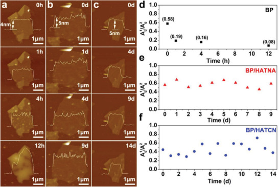
The ambient stability of BP and BP/HATs. a–c) AFM images and d–f) Raman spectra of a BP, BP/HATNA, and BP/HATCN sheets exposed in air for different days.
The “built‐in” electric field at the BP/HATs interfaces, similar to that of graphene/tetrafluoro‐tetracyanoquinodimethane (F4‐TCNQ) complex,[ 32 , 39 ] provides an opportunity to modulate the band structure of BP sheets, depending on the adsorbed density of HATs. The optical band gap (E g) and the valence band edge (E v) of BP and BP/HATs were investigated by ultraviolet–visible (UV/Vis) absorption spectroscopy and ultraviolet photoelectron spectroscopy (UPS), respectively (Figures S14–S17, Supporting Information). The conduction bands (E c) of BP and BP/HATs were calculated by the equation E c = E v + E g. As depicted in Figure 4a , E g and E v of the pristine BP are 0.9 and ‐4.85 eV, respectively. Notably, E g and E v of BP/HATs are tunable according to the HATs concentrations (C). For example, in BP/HATNA, E g significantly decreases from 0.64 to 0.48 eV when C HATNA increases from 0.01 to 0.5 mg mL‐1, while E v shifts from ‐5.97 eV down to ‐7.81 eV. The further increase of C HATNA above 0.5 mg mL‐1 gives rise to a minimal E g of 0.46 eV and E v of ‐7.98 eV. This is probably associated with the fully molecular coverage at the BP surfaces that achieves a maximum “built‐in” electric field. Compared with BP/HATNA, the E g of BP/HATCN is reduced to 0.21 eV, and its E v shifts down to ‐6.31 eV at C HATCN = 0.01 mg mL‐1, because of the stronger interaction between lone electron pairs of BP and rich cyano groups of HATCN. Furthermore, the E g and E v of BP/HATCN present a similar trend as BP/HATNA. When the HATCN concentration reaches 2 mg mL‐1, the E g and E v of BP/HATCN achieve minimal values of 0.13 and ‐7.80 eV, respectively.
Figure 4.

The band structures of BP and BP/HATs. a) The band structures of BP, BP/HATNA, and BP/HATCN with the variation of HATs concentrations from 0.01 to 2 mg mL‐1. b–d) Band structures and projected densities of states for BP, BP/HATNA, and BP/HATCN, respectively.
The band structures of BP and BP/HATs are further studied by first‐principle calculations (Figure 4b–d and Figures S18 and S19, Supporting Information). We selected monolayer BP as the model material to simplify the calculation process, as opposed to the few‐layer BP used in the experiments. To exclude the possible interaction between HATs molecules, we took one HATs molecule per 5.7 square nanometer of BP lattice as the loading density for the calculation. As a result, pristine BP is a direct gap semiconductor with a bandgap of 0.85 eV at Γ point, consistent with the calculated results from the literature.[ 40 ] After functionalization, the band gaps of BP/HATs are significantly decreased to 0.52 and 0.14 eV by using HATNA and HATCN, respectively, which support the experimental results. We found that the narrower bandgaps of BP/HATs result from the flat energy levels close to the Fermi levels (E F). To gain a deeper insight into the emerging flat bands, the density of states (DOS) and the projected density of states (PDOS) of BP and BP/HATs were studied. As shown in Figure 4c,d, the flat band originates primarily from the adsorbed HATs molecules and is almost independent of BP. Such flat bands are the localized electronic states, which act as acceptor states in BP/HATs systems and facilitate the electron transfer process from BP to HATs.[ 41 , 42 ]
To understand the effect of HATs functionalization on the charge carrier transport properties of BP sheets, we employed optical‐pump THz‐probe (OPTP) spectroscopy to investigate time‐ and frequency‐resolved photoconductivity of pristine BP and BP/HATs films. As schematically shown in Figure 5a , following optical excitations by ≈3.1 eV (400 nm) ultrafast laser pulses, we optically inject charge carriers into the samples. The photoconductivity (Δσ) is subsequently probed by a single‐cycle THz pulse (≈1 ps duration) to measure the pump‐induced and relative change in the transmitted electrical field (E), following: Δσ ∝ (see Supporting Information for details). In Figure 5b, we compare the photoconductivity dynamics of the three samples divided by the incident photon density. Upon photoexcitation, they all exhibit an ultrafast rise in the photoconductivity, due to the optically injected free charge carriers, followed by a relaxation process on the order of tens of ps. Remarkably, the photoconductivity of BP/HATs is much higher than that of pristine BP under the same incident photon density, indicating substantially enhanced charge mobility in BP/HATs. Moreover, HATs enhance the lifetime of charge carriers in BP, as clearly demonstrated in the normalized dynamics in Figure 5c. The averaged carrier lifetimes (see detailed discussion in Supporting Information) follow a trend: t BP (≈14 ps) <t BP/HATCN (≈32 ps) <t BP/HATNA (≈42 ps). For pristine BP, it has been well‐known that oxidation can take place at BP surfaces owing to abundant lone pair electrons. This leads to the generation of unavoidable defect states in BP. As we demonstrated in Figure 4a,b, HATs coating can effectively protect BP from oxidation by decreasing its surface electron density. As such, HAT treatments not only extend the lifetime but also enhance the mobility of photogenerated charge carriers in BPs.
Figure 5.

THz studies on the microscopic charge carrier transport properties of BP and BP/HATs films. a) Illustration of optical‐pump THz‐probe (OPTP) spectroscopy. b) Photoconductivity dynamics of BP, BP/HATCN, and BP/HATNA normalized to the incident photon density. Samples are excited by a pulsed laser with a photon energy of ≈3.1 eV and an incident photon density of 3.8 × 1012 cm‐2 under a dry nitrogen environment. c) Normalized photoconductivity dynamics based on the data in (b). Solid lines are biexponential fits to the data (see Supporting Information). d–f) Frequency‐resolved complex THz photoconductivity (measured at 2 ps after the maximum photoexcitation) for BP, BP/HATNA, and BP/HATCN films, respectively. The solid lines correspond to the Drude‐Smith fits to the data.
To further elucidate the origin of the enhanced photoconductivity in BP/HATs, we measured the frequency‐resolved complex THz photoconductivity dynamics of HATNA, HATCN, BP, and BP/HATs at ≈2 ps after the maximum photoconductivity. For comparison, the HAT molecules themselves do not present any photoconductivity (Figure S20, Supporting Information). As shown in Figure 5d–f, the obtained frequency‐resolved complex THz photoconductivity of BP and BP/HATs can be well‐fitted by the Drude‐Smith model (see SI for details), which describes the confined transport of charge carriers as a result of spatial confinement (e.g., grain boundary and structural configuration). According to the Drude‐Smith fits, BP, BP/HATCN, and BP/HATNA exhibit effective scattering times of τBP = 35 ± 5 fs, τBP/HATCN = 58 ± 3 fs and τBP/HATNA = 88 ± 3 fs, respectively. The longer scattering times for BP/HATs reflect the observed higher photoconductivity in both samples compared to the pristine BP due to lower defect density following the discussion in the last section. We selected the effective mass of 5‐layer BP (m* = 0.19 m 0)[ 43 ] from the reference to evaluate the trend of the mobility improvement for BP/HATs because the BP sheets we used in this work are about five layers, and the effective masses of the BP and BP/HATs at such thicknesses are expected to be very similar. The charge mobilities (, see details in Supporting Information) of BP, BP/HATCN, and BP/HATNA films in the dc limit are 35 ± 5, 69 ± 3, and 97 ± 3 cm2 V‐1 s‐1, respectively. Note that, the long‐range charge transport in the films is suppressed due to the difficulty for charge carriers to migrate between the individual BP flakes. Still, the charge mobility of BP/HATNA films represents one of the highest values for BP sheets and other conventional inorganic 2D materials prepared by liquid‐phase exfoliation (Tables S4–S6, Supporting Information). The ambient stability of the electronic properties of BP and BP/HATs was further studied by OPTP spectroscopy. We select a high incident photon density of 3.2 × 1014 cm‐2 in air to accelerate their potential degradation processes, as opposed to the much lower incident photon density of 3.8 × 1012 cm‐2 that we used to characterize their charge transport properties (see details in Supporting Information). As shown in Figure S21 (Supporting Information), BP/HATs exhibit stable photoconductivity during high‐power illumination in air, whereas BP shows a substantial decrease in photoconductivity up to ≈90 %. This result further demonstrates the superior stability of BP/HATs, and it is in good agreement with the AFM and Raman characterizations.
3. Conclusion
In summary, we have demonstrated a molecular engineering strategy to prepare ambient stable BP/HAT hybrid heterostructures. This strategy not only modifies the band structure of BP sheets but also improves their charge mobility. HATs serve as electron acceptors that withdraw lone pair electrons from P atoms, resulting in a strong charge transfer from BP surface to HAT layer and leading to an improved ambient stability of BP/HAT sheets for up to 21 d. THz spectroscopic studies reveal that HATs substantially extend the scattering time of BP/HATs and yield a charge carrier mobility of 97 ± 3 cm2 V‐1 s‐1 for BP/HATNA film, which is much higher than that of the pristine BP film (35 ± 5 cm2 V‐1 s‐1). Our strategy provides a nondestructive pathway to protect BP sheets from degradation and to tailor their electronic properties. The future endeavor to synthesize novel organic molecules and/or other air‐sensitive 2D materials can greatly expand the family of such hybrid molecular heterostructures with a variety of unprecedented new functions.
Conflict of Interest
The authors declare no conflict of interest.
Supporting information
Supporting information
Acknowledgements
H.S., S.F., and Y.L. contributed equally to this work. This work was financially supported by Deutsche Forschungsgemeinschaft (MX‐OSMOPED project), ERC Consolidator Grant on T2DCP, M‐ERA‐NET project HYSUCAP, SPES3 project funded by German Ministry for Education and Research (BMBF) under Forschung für neue Mikroelektronik (ForMikro) program and GrapheneCore3 881603. The authors thank Dr. Panpan Zhang, Dr. Zaichun Liu, Dr. Libo Ma, Dr. Kejun Liu, Dr. Haoyuan Qi, Dr. Zhen Zhang, and Dr. Markus Löffler for helpful discussions and characterization, and also acknowledge the Center for Advancing Electronics Dresden (cfaed), the Dresden Center for Nanoanalysis (DCN). Y.L. also acknowledges the Centre for Information Services and High Performance Computing (ZIH) in Dresden, Germany, for the provided computational resources. In addition, the authors acknowledge the support of computational calculations from Chenghao Liu in McGill University, Canada. H.S. and S.F. thank China Scholarship Council (CSC) for financial support. C.N. and A.T. acknowledge the financial support by FLAG‐ERA “H2O” Project (DFG TU149/9‐1) and SPP 2244 “2DMP” (DFG TU149/13‐1).
Open access funding enabled and organized by Projekt DEAL.
Shi H., Fu S., Liu Y., Neumann C., Wang M., Dong H., Kot P., Bonn M., Wang H. I., Turchanin A., Schmidt O. G., Shaygan A. Nia, Yang S., Feng X., Molecularly Engineered Black Phosphorus Heterostructures with Improved Ambient Stability and Enhanced Charge Carrier Mobility. Adv. Mater. 2021, 33, 2105694. 10.1002/adma.202105694
Contributor Information
Hai I. Wang, Email: wanghai@mpip-mainz.mpg.de.
Ali Shaygan Nia, Email: ali.shaygan_nia@tu-dresden.de.
Sheng Yang, Email: s.yang@fkf.mpg.de.
Xinliang Feng, Email: xinliang.feng@tu-dresden.de.
Data Availability Statement
Research data are not shared.
References
- 1. Youngblood N., Chen C., Koester S. J., Li M., Nature Photon. 2015, 9, 247. [Google Scholar]
- 2. Woomer A. H., Farnsworth T. W., Hu J., Wells R. A., Donley C. L., Warren S. C., ACS Nano 2015, 9, 8869. [DOI] [PubMed] [Google Scholar]
- 3. Li L., Yu Y., Ye G. J., Ge Q., Ou X., Wu H., Feng D., Chen X. H., Zhang Y., Nat. Nanotechnol. 2014, 9, 372. [DOI] [PubMed] [Google Scholar]
- 4. Ge S., Li C., Zhang Z., Zhang C., Zhang Y., Qiu J., Wang Q., Liu J., Jia S., Feng J., Sun D., Nano Lett. 2015, 15, 4650. [DOI] [PubMed] [Google Scholar]
- 5. Perello D. J., Chae S. H., Song S., Lee Y. H., Nat. Commun. 2015, 6, 7809. [DOI] [PMC free article] [PubMed] [Google Scholar]
- 6. Yuan H., Liu X., Afshinmanesh F., Li W., Xu G., Sun J., Lian B., Curto A. G., Ye G., Hikita Y., Shen Z., Zhang S.‐C., Chen X., Brongersma M., Hwang H. Y., Cui Y., Nat. Nanotechnol. 2015, 10, 707. [DOI] [PubMed] [Google Scholar]
- 7. Zhou Q., Chen Q., Tong Y., Wang J., Angew. Chem., Int. Ed. 2016, 55, 11437. [DOI] [PubMed] [Google Scholar]
- 8. Plutnar J., Sofer Z., Pumera M., ACS Nano 2018, 12, 8390. [DOI] [PubMed] [Google Scholar]
- 9. Wood J. D., Wells S. A., Jariwala D., Chen K.‐S., Cho E., Sangwan V. K., Liu X., Lauhon L. J., Marks T. J., Hersam M. C., Nano Lett. 2014, 14, 6964. [DOI] [PubMed] [Google Scholar]
- 10. Uk Lee H., Lee S. C., Won J., B.‐C. Son,, Choi S., Kim Y., Park S. Y., Kim H.‐S., Lee Y.‐C., Lee J., Sci. Rep. 2015, 5, 8691. [DOI] [PMC free article] [PubMed] [Google Scholar]
- 11. Doganov R. A., O'Farrell E. C. T., Koenig S. P., Yeo Y., Ziletti A., Carvalho A., Campbell D. K., Coker D. F., Watanabe K., Taniguchi T., Neto A. H. C., Özyilmaz B., Nat. Commun. 2015, 6, 6647. [DOI] [PubMed] [Google Scholar]
- 12. Kim J., Baek S. K., Kim K. S., Chang Y. J., Choi E. J., Curr. Appl. Phys. 2016, 16, 165. [Google Scholar]
- 13. Ryder C. R., Wood J. D., Wells S. A., Yang Y., Jariwala D., Marks T. J., Schatz G. C., Hersam M. C., Nat. Chem. 2016, 8, 597. [DOI] [PubMed] [Google Scholar]
- 14. Walz Mitra K. L., Chang C. H., Hanrahan M. P., Yang J., Tofan D., Holden W. M., Govind N., Seidler G. T., Rossini A. J., Velian A., Angew. Chem., Int. Ed. 2021, 60, 9127. [DOI] [PubMed] [Google Scholar]
- 15. Sofer Z., Luxa J., Bouša D., Sedmidubský D., Lazar P., Hartman T., Hardtdegen H., Pumera M., Angew. Chem., Int. Ed. 2017, 56, 9891. [DOI] [PubMed] [Google Scholar]
- 16. Liu X., Xiao L., Weng J., Xu Q., Li W., Zhao C., Xu J., Zhao Y., Sci. Adv. 2020, 6, eabb4359. [DOI] [PMC free article] [PubMed] [Google Scholar]
- 17. Tofan D., Sakazaki Y., Walz Mitra K. L., Peng R., Lee S., Li M., Velian A., Angew. Chem., Int. Ed. 2021, 60, 8329. [DOI] [PubMed] [Google Scholar]
- 18. Sluysmans D., Lussis P., Fustin C.‐A., Bertocco A., Leigh D. A., Duwez A.‐S., J. Am. Chem. Soc. 2021, 143, 2348. [DOI] [PubMed] [Google Scholar]
- 19. Dai Y., Zhang H., Zhang Z., Liu Y., Chen J., Ma D., J. Mater. Chem. C 2015, 3, 6809. [Google Scholar]
- 20. Ding L., Sun Y., Chen H., Zu F., Wang Z., Liao L., J. Mater. Chem. C 2014, 2, 10403. [Google Scholar]
- 21. Zhao D., Zhu Z., Kuo M.‐Y., Chueh C.‐C., Jen A. K. Y., Angew. Chem., Int. Ed. 2016, 55, 8999. [DOI] [PubMed] [Google Scholar]
- 22. Yoshida H., Yoshizaki K., Org. Electron. 2015, 20, 24. [Google Scholar]
- 23. Kaafarani B. R., Kondo T., Yu J., Zhang Q., Dattilo D., Risko C., Jones S. C., Barlow S., Domercq B., Amy F., Kahn A., Brédas J.‐L., Kippelen B., Marder S. R., J. Am. Chem. Soc. 2005, 127, 16358. [DOI] [PubMed] [Google Scholar]
- 24. Kobylarczyk J., Pinkowicz D., Srebro‐Hooper M., Hooper J., Podgajny R., Dalton Trans. 2017, 46, 3482. [DOI] [PubMed] [Google Scholar]
- 25. Yang S., Zhang K., Ricciardulli A. G., Zhang P., Liao Z., Lohe M. R., Zschech E., Blom P. W. M., Pisula W., Müllen K., Feng X., Angew. Chem., Int. Ed. 2018, 57, 4677. [DOI] [PubMed] [Google Scholar]
- 26. Zhang Z., Zhang P., Yang S., Zhang T., Löffler M., Shi H., Lohe M. R., Feng X., Proc. Natl. Acad. Sci. USA 2020, 117, 13959. [DOI] [PMC free article] [PubMed] [Google Scholar]
- 27. Shi H., Li M., Nia A. S., Wang M., Park S., Zhang Z., Lohe M. R., Yang S., Feng X., Adv. Mater. 2020, 32, 1907244. [DOI] [PubMed] [Google Scholar]
- 28. Yang S., Chen G., Ricciardulli A. G., Zhang P., Zhang Z., Shi H., Ma J., Zhang J., Blom P. W. M., Feng X., Angew. Chem., Int. Ed. 2020, 59, 465. [DOI] [PMC free article] [PubMed] [Google Scholar]
- 29. Zhu X., Zhang T., Jiang D., Duan H., Sun Z., Zhang M., Jin H., Guan R., Liu Y., Chen M., Ji H., Du P., Yan W., Wei S., Lu Y., Yang S., Nat. Commun. 2018, 9, 4177. [DOI] [PMC free article] [PubMed] [Google Scholar]
- 30. Tan S. J. R., Abdelwahab I., Chu L., Poh S. M., Liu Y., Lu J., Chen W., Loh K. P., Adv. Mater. 2018, 30, 1704619. [DOI] [PubMed] [Google Scholar]
- 31. Wang S., Li J., Zhao Y., Liu B., Yuan P., Wei J., Zhang J., Xie H., Niu D., Long M., Gao Y., Appl. Phys. Lett. 2020, 117, 061602. [Google Scholar]
- 32. Chen W., Chen S., Qi D. C., Gao X. Y., Wee A. T. S., J. Am. Chem. Soc. 2007, 129, 10418. [DOI] [PubMed] [Google Scholar]
- 33. Khalil L., Pierucci D., Papalazarou E., Chaste J., Silly M. G., Sirotti F., Eddrief M., Perfetti L., Lhuillier E., Ouerghi A., Phys. Rev. Mater. 2019, 3, 084002. [Google Scholar]
- 34. Tang W., Sanville E., Henkelman G., J. Phys. Condens. Matter 2009, 21, 084204. [DOI] [PubMed] [Google Scholar]
- 35. Sanville E., Kenny S. D., Smith R., Henkelman G., J. Comput. Chem. 2007, 28, 899. [DOI] [PubMed] [Google Scholar]
- 36. Del Rio Castillo A. E., Pellegrini V., Sun H., Buha J., Dinh D. A., Lago E., Ansaldo A., Capasso A., Manna L., Bonaccorso F., Chem. Mater. 2018, 30, 506. [Google Scholar]
- 37. Wang Y., Slassi A., Cornil J., Beljonne D., Samorì P., Small 2019, 15, 1903432. [DOI] [PubMed] [Google Scholar]
- 38. Favron A., Gaufrès E., Fossard F., Phaneuf‐L'Heureux A.‐L., Tang N. Y. W., Lévesque P. L., Loiseau A., Leonelli R., Francoeur S., Martel R., Nat. Mater. 2015, 14, 826. [DOI] [PubMed] [Google Scholar]
- 39. Coletti C., Riedl C., Lee D. S., Krauss B., Patthey L., von Klitzing K., Smet J. H., Starke U., Phys. Rev. B 2010, 81, 235401. [Google Scholar]
- 40. Wang Q. H., Kalantar‐Zadeh K., Kis A., Coleman J. N., Strano M. S., Nat. Nanotechnol. 2012, 7, 699. [DOI] [PubMed] [Google Scholar]
- 41. Xia F., Xiong S., He Y., Shao Z., Zhang X., Jie J., J. Phys. Chem. C 2017, 121, 19530. [Google Scholar]
- 42. Jing Y., Tan X., Zhou Z., Shen P., J. Mater. Chem. A 2014, 2, 16892. [Google Scholar]
- 43. Qiao J., Kong X., Hu Z.‐X., Yang F., Ji W., Nat. Commun. 2014, 5, 4475. [DOI] [PMC free article] [PubMed] [Google Scholar]
Associated Data
This section collects any data citations, data availability statements, or supplementary materials included in this article.
Supplementary Materials
Supporting information
Data Availability Statement
Research data are not shared.