Abstract
Precise manipulation of light–matter interactions has enabled a wide variety of approaches to create bright and vivid structural colors. Techniques utilizing photonic crystals, Fabry–Pérot cavities, plasmonics, or high‐refractive‐index dielectric metasurfaces have been studied for applications ranging from optical coatings to reflective displays. However, complicated fabrication procedures for sub‐wavelength nanostructures, limited active areas, and inherent absence of tunability of these approaches impede their further development toward flexible, large‐scale, and switchable devices compatible with facile and cost‐effective production. Here, a novel method is presented to generate structural color images based on monochromic conducting polymer films prepared on metallic surfaces via vapor phase polymerization and ultraviolet (UV) light patterning. Varying the UV dose enables synergistic control of both nanoscale film thickness and polymer permittivity, which generates controllable structural colors from violet to red. Together with grayscale photomasks this enables facile fabrication of high‐resolution structural color images. Dynamic tuning of colored surfaces and images via electrochemical modulation of the polymer redox state is further demonstrated. The simple structure, facile fabrication, wide color gamut, and dynamic color tuning make this concept competitive for applications like multifunctional displays.
Keywords: poly[3,4‐ethylenedioxythiophene]; redox‐tunable; structural colors; UV patterning
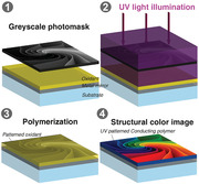
A UV‐light patterning method turns monochromic conducting polymers into multicolor images, using the UV dose to control structural coloration via both the film thickness and polymer permittivity. Electrochemical modulation of the conducting polymer redox states further enables dynamic tuning of the structurally colored images.
1. Introduction
Layered nanoscale thin‐film structures, exemplified by Fabry–Pérot cavities[ 1 , 2 , 3 ] and ultrathin lossy films on metal mirrors,[ 4 ] can produce reflective structural colors based on interference effects instead of conventional material absorption as for pigments and dyes.[ 5 ] Such structural coloration can offer various attractive features, including intrinsic resistance to fading, excellent durability, bright colors under direct sunlight, and possibility for high resolution images.[ 4 , 5 , 6 ] Combined with means for dynamic tuning, structural colors show potential for smart labels and electronic paper in color,[ 7 ] with promise for ultralow power consumption, wide color range, compact device structures, and high switching speeds.[ 2 , 8 ] Recent efforts to facilitate tuning or on/off switching of structural colors have combined optical nanocavities with conducting polymers, whose optical transparency can be controlled electrochemically.[ 1 , 9 , 10 ] The same redox dependence has made conducting polymers popular for electrochromic displays also without cavities, but typically limited to monochromic function.[ 11 , 12 , 13 ] As example, the popular conducting polymer PEDOT (poly[3,4‐ethylenedioxythiophene]) switches only between different shades of blue, while practical applications would preferably also cover other parts of the spectrum.[ 14 ] Here, we address this issue and show that the monochromic conducting polymer PEDOT:Tosylate (PEDOT:Tos, see chemical structure in Figure 1b) can generate colors across the whole visible if deposited at accurate nanoscale thicknesses on a metal mirror (illustrated in Figure 1a). We achieve such thickness control using a UV exposure step of the oxidant precursors before film formation via vapor phase polymerization (VPP, see details in Experimental section).[ 11 , 15 , 16 , 17 , 18 ] UV exposure through grayscale photomasks thereby enables simple production of structural color images at high resolution (down to 10 µm[ 15 ]), which are further dynamically tuneable via the polymers’ intrinsic redox properties.[ 15 , 19 ] Optical simulations match the experimental results and reveal that the coloration originates from thin‐film interference effects. However, by contrast to the common way to control structural colors via geometry (i.e., film thickness),[ 1 , 20 ] we demonstrate that the UV‐treatment simultaneously modulates both thickness and complex permittivity of the conducting polymer. In turn, the additional permittivity variation promotes the tuning and quality of the structural colors via several synergistic effects, as explored and discussed in detail. The novel approach to control structural colors jointly via geometry and material properties may open new avenues also for systems based on other materials.
Figure 1.
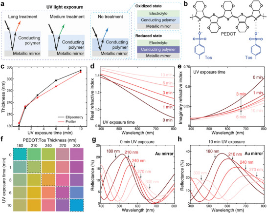
The concept of structural colors based on UV‐treated conducting polymer thin films on metal surfaces. a) Schematics of the basic device structure, for which different doses of UV light treatment tunes both the thickness and the complex refractive index of the conducting polymer films, leading to generation of different structural colours in reflection. By depositing a layer of electrolyte on top, the reflected colors of the devices can be further tuned by controlling the conducting polymer redox state (reduced and oxidized states). b) Chemical structure of PEDOT:Tos. c) Thickness and d,e) in‐plane real (d) and imaginary (e) refractive index of PEDOT:Tos films based on different UV exposure times (0, 1, 3, 6, and 10 min) and VPP time of 60 min. The thickness values were determined by both spectroscopic ellipsometry and profiler. f) Simulated pseudo‐colors of devices with different UV exposure times (different permittivity) and thicknesses. g,h) Simulated reflectance curves of devices with 0 min (g) and 10 min (h) UV treatment. In the simulation, Au with thickness of 100 nm was used as the metallic mirror.
2. Results and Discussion
In accordance with previous studies,[ 15 ] the thickness of our conducting polymer films could be readily controlled at the nanoscale and altered from 180 to 320 nm (Figure 1c) by varying only the UV exposure time of the spin‐coated oxidant before VPP, and keeping other parameters fixed (see Experimental Section for details). Ellipsometry measurements (Figures S1 and S2, Supporting Information) reveal that the thickness variation is accompanied by gradual variation in the complex refractive index of the conducting polymer films (Figure 1d,e). We observe significant changes in the in‐plane real refractive index in the red and near infrared (NIR) regions (see Figure S2, Supporting Information for the out‐of‐plane data), with increasing values for longer UV exposure times. The imaginary component instead shows a significant decrease at long wavelengths upon UV exposure, and a tendency of slightly enhanced values at shorter wavelengths. These results agree with measured extinction spectra (Figure S3, Supporting Information).
Numerical simulations predict that the conducting polymer thin films should be able to generate vibrant reflective structural colors if placed on a gold (Au) mirror (Figure 1f). The structural colors vary both with (UV‐induced) permittivity modulation and polymer thickness. Using the UV‐exposure approach, we can simultaneously vary both those properties, which corresponds to the diagonal of the pseudo‐color palette presented in Figure 1f. Such simultaneous modulation leads to improved color tuning due to several synergistic effects. First, the reflectance peak is redshifted not only by the increasing thickness, but also by the UV‐induced increase in real permittivity. As a result, long‐wavelength resonances can be generated at lower thicknesses (Figure 1g,h), which leads to reduced absorption losses. At the same time, the large reduction in imaginary permittivity upon UV light exposure suppresses absorption at long wavelengths, which further aids the generation of yellow and red colors upon UV‐treatment. Figure 1h also shows that the bluish structural color for the longest UV exposure time (bottom right in Figure 1f) is due to a second order reflectance peak emerging at shorter wavelengths. Again, the UV exposure reduces the influence of this feature compared with only varying the thickness, both by allowing higher reflection for the primary red peak and also by increasing the spectral distance between the first and second order peaks by reducing the negative slope of the real permittivity (also see Figures S6 and S7, Supporting Information). Altogether, UV‐induced tuning of the conducting polymer thin film provides several effects that work together to improve the color gamut of the system.
We experimentally prepared nanoscale PEDOT:Tos films on Au mirrors using different UV exposure times (0, 1, 3, 6, and 10 min) of the oxidant before VPP (Figure 2a). The resulting reflectance spectra are presented in Figure 2b (solid lines) together with simulated results (dashed lines). Devices with 30 min VPP PEDOT:Tos films exhibited colors from blue‐green to orange, while a further increase of polymerization time to 60 min pushed the colors further into the red, with a reflectance peak at around 670 nm for the 10 min UV‐treated sample. Converting the spectra to CIE chromaticity coordinates indicates good color tuneability (Figure 2c). As discussed above, the purity of the red colors is somewhat limited due to the secondary peak in the blue, although to a lesser extent compared with only tuning the thickness. We also note a limited coverage in the blue region, which is due to interband transitions of Au and corresponding limited reflection of the bottom mirror at short wavelengths. Although silver (Ag) or aluminum (Al) mirrors would provide improved reflection at short wavelengths, they led to poor polymer film coverage due to chemical reactions with the precursors (Figure S4, Supporting Information). To jointly optimize mirror properties and polymer film quality, we therefore replaced the Au mirror with 100 nm Al topped with a 3 nm Cr adhesion layer and only a very thin Au layer (7 nm, see mirror reflection spectra in Figure S5, Supporting Information). Figure 2d presents reflection spectra for UV‐treated PEDOT:Tos films prepared on this new Al/Cr/Au mirror, indeed revealing a broad structural color range that includes blue and violet‐blue. The first order reflectance peak could be tuned from 410 to 660 nm, almost covering the whole visible range as also clear from the CIE chromaticity diagram (Figure 2e). Numerical simulations for additional polymer thicknesses confirm these findings (Figures S6 and S7, Supporting Information). As predicted above, the color gamut obtained by UV exposure (i.e., combined nanoscale modulation of both thickness and permittivity) was better than expected based on only variations in film thickness (Figures S8 and S9, Supporting Information). The devices showed clear but relatively low angle dependence, with only small shifts in reflectance peak positions for incident angles below 40° (Figures S10 and S11, Supporting Information). In addition to UV exposure and polymerization times, other processing parameters, including precursor recipe, could also be used to modulate the final structural colors (Figure S12, Supporting Information). In Note A, Supporting Information, we particularly discuss effects of UV exposure on surface roughness and how an additional annealing step could reduce roughness while reducing tuneability.
Figure 2.
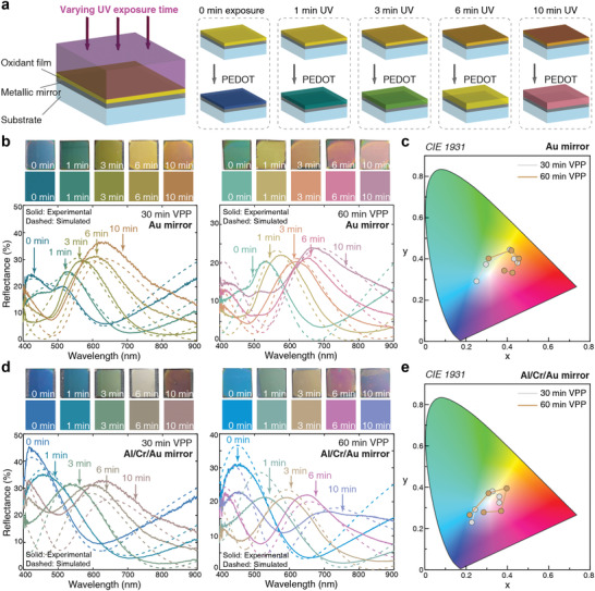
Experimental demonstration of UV‐light‐controlled structural colors. a) Fabrication of UV‐treated PEDOT by different UV light exposure times. b,d) Devices made by UV‐treated PEDOT films with various exposure times on 100 nm Au mirrors (b) and 7 nm Au/3 nm Cr/100 nm Al mirrors (d) and c,e) their corresponding coordinates distribution in the CIE 1931 chromaticity diagram. Five UV exposure times were used: 0, 1, 3, 6, and 10 min. In (b) and (d), the left column is for 30 min VPP and the right for 60 min VPP; the panels on top of each graph show sample photographs (with size of 2.5 cm by 2.5 cm) in the first row and pseudocolors obtained from their CIE coordinates based on experimental reflectance curves in the second row. The solid lines are experimental data while the dashed ones were obtained from numerical simulations.
The effect of UV treatment on the conducting polymer is determined by the total UV dose,[ 15 ] which means that nanoscale modulation of polymer thickness and permittivity can be controlled via the UV light intensity in addition to exposure time. Similar strategies recently enabled fabrication of grayscale electrochromic polymer devices.[ 11 , 12 ] For our structurally colored devices, insertion of grayscale photomasks during UV exposure should enable the production of multiple colors on the same substrate using just a single exposure step (Figure 3a). To verify this, we used grayscale photomasks with both pixels and gradient bar patterns that were printed on transparent plastic films by normal office printers (Figure 3b). We used four pixels with transmittance varying from above 70% to below 1% at 405 nm, the wavelength of the UV light source. 1 min UV exposure time (30 min VPP on Al/Cr/Au mirrors) led to only moderate variations in color between the different pixels and across the gradient bars (Figure 3c). By contrast, longer exposure times (presented for 6 and 10 min in Figure 3d,e, respectively) enabled production of colors from blue to red on the same device (also see Figure S13, Supporting Information). With a single UV exposure, the concept managed to generate all three primary RGB colors, and the gradient bars further illustrate the possibility for gradual fine‐tuning of the structural colors across the visible along the sample surface.
Figure 3.
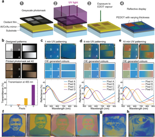
Reflective structural color images based on UV‐patterned PEDOT on Al/Cr/Au mirrors. a) Schematic process flow of the UV patterning technique. b) Designed grayscale patterns with separate pixels and gradient bars (top), photographs of printed photomasks (middle, set #2, set #1 and #3 are shown in Figure S13, Supporting Information), and corresponding transmittance of pixel A‐D at 405 nm (bottom). c–e), UV‐patterned PEDOT devices using the printed photomask set #2 at different UV exposure times (1, 6, and 10 min). The polymerization time was 30 min. The first, second, and third rows are device images, CIE pseudocolors, and reflectance curves, respectively. The different pixels (A to D) are indicated in both device photographs and CIE generated color images. f–h) UV‐patterned PEDOT devices made using gray‐scale photomasks of one of the co‐authors (f), a cat (g), and an eye (h). The image of the author in (f) appears here with their consent. The different images in (f) correspond to different UV exposure and polymerization times using the same photomask, showing the possibility to tailor the structural colored images.
We then utilized grayscale images as photomasks (Figure 3f–h and Figure S14, Supporting Information), which resulted in multicolored pictures that precisely reproduced the original photomasks. Varying the UV patterning or polymerization time, we were able to further alter the color map of the same picture. Compared with other approaches to generate structurally colored images, the one‐step UV patterning approach reduces fabrication complexity and offers large‐scale production with good color quality, good tuneability, and high resolution without need for expensive equipment. There is also plenty of room for studying and further improving the concept by varying different parameters, including the bottom mirror, conducting polymers, wavelengths and intensity of the UV light, and other possible precursor deposition methods (e.g., ink jet and spray printing). The simple structure and facile fabrication process also permit us to form images on flexible substrates. Devices made on Au‐coated poly(ethylene terephthalate) substrates showed high quality and durability with no observable damage upon bending (Figure S25, Supporting Information), meeting the requirements of large‐area flexibility for wearable and biomedical electronics.[ 10 ] The fact that the oxidant can also be deposited by printing techniques, such as screen printing,[ 21 ] shows further promise of the UV patterning approach for scalable production of fully printed devices.
To unveil the mechanisms involved in generating structural colors with conducting polymer thin films on metal mirrors, we analyze the electric field and absorbed power distributions for a device with 170 nm thick 0 min UV‐treated PEDOT film on the Al/Cr/Au mirror (Figure 4a). The device generates a standing‐wave pattern above the polymer film that is significantly stronger at the reflection peak than at the reflection minimum (Figure 4b). The results are associated with lower absorption by the cavity at the reflectance maximum than at the reflectance minimum, which also shows predominant absorption in the top part of the polymer film where the electric field is higher (Figure 4c). Similar results were found for devices made of PEDOT:Tos at other thicknesses and treated at different UV exposure times (Figure S15, Supporting Information), with field and absorption distributions varying with resonance order. Combined with the observed redshift with increasing thickness and refractive index, the trends are similar for those expected based on constructive interference between light reflected by the air/polymer interface and the polymer/metal interface, although the air/polymer interface has relatively low reflectance (less than 4% in the visible, see Figure S16, Supporting Information). In that respect we note that the interference pattern remains also if the same device is immersed in water, which further reduces the reflection at the first (water/polymer) interface to less than 2% in the lower part of the spectrum (Figure S16, Supporting Information). While lowered magnitude of the fringe pattern indicates reduced interference, the sample in water still generates largely the same spectral lineshape, electric field, and absorbed power distributions as the sample in air (Figure 4d–f). We further note that our partly lossy polymer system resembles a broadband absorber cavity,[ 22 ] implying that the effects also relate to modulation of the polymer absorption by wavelength‐dependent standing waves formed between incident light and light reflected by the bottom mirror. These findings are of high relevance for practical applications, because they suggest that we can immerse the devices in electrolytes with only little suppression of the structural colors. In turn, electrolyte immersion should enable electrochemical tuning of the redox state of the polymer thin films and corresponding in situ control of the optical response of the devices.
Figure 4.
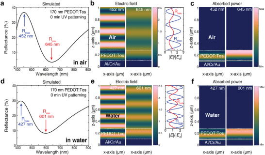
Coloration mechanism for PEDOT:Tos thin films on metal mirrors. A device made of 170 nm PEDOT:Tos without UV exposure was used as model system: a) Reflectance spectrum for the device in air. b) Electric field distribution at the reflectance maximum (452 nm) and reflectance minimum (645 nm), and the relative electric field strength along the z‐axis above the PEDOT:Tos film. c) Absorbed power distribution at the same two wavelengths. d–f) Simulated results for an identical device as in (a–c) but with water as surrounding medium instead of air, with reflectance spectrum (d), electric field distributions (e), and absorbed power distributions (f). The interfaces of air or water/PEDOT:Tos, and PEDOT:Tos/metallic mirror are indicated by white dashed lines in the field plots.
For in situ electrochemical switching, we inserted structurally colored devices (using Au mirrors to ensure electrochemical stability) into a flow cell (Figure 5a) filled with electrolyte (1 m KCl aq.). We connected the devices to the working electrode (W.E.) and used a platinum (Pt) electrode as both counter and reference electrode (C.E. and R.E.) in a two‐electrode setup. Electrochemical cyclic voltammetry showed rectangular shapes for conducting polymer films (homogenous films, not patterned) treated at different UV exposure times (Figure 5b and Figure S17, Supporting Information). The asymmetry for the 10 min UV sample and pinch‐off at negative bias could be due to weakened redox‐tunability of samples after prolonged UV exposure.[ 12 ] By applying a positive bias to the devices, we could oxidize (or dope) the conducting polymer films, and thus reduce the absorption in the visible (Figure S18, Supporting Information). This modulation led to increased reflectance and brighter structural colors for both UV‐treated and non‐treated devices (Figure 5c–e). On the contrary, applying a negative bias reduces (or dedopes) the polymer, which results in enhanced absorption in visible and reduced absorption in the NIR. Such negative bias therefore dimmed the devices, which presented dark red or brown colors (Figure 5c and Figure S18, Supporting Information). In addition to the modulation of the polymer absorption, possible variations in polymer film thickness upon electrochemical switching may also play a role in the observed variations of the optical response. Devices using Al/Cr/Au mirrors showed improved color tunability, with color changing from green to purple, and finally to red, although with the disadvantage of deteriorating in the electrochemical environment (Figure S19, Supporting Information). Regardless of mirror‐type, the change of reflectance and device color occurred within seconds. When removing the bias, the samples slowly returned to their original state, with variations for different UV exposure times (or electrical/ionic conductivity). In addition to the electrochemically induced reflectance modulation (as demonstrated in Figure 4d), we observed a redshift of the color when the environment of the devices changed from air to water, especially for samples with longer UV treatment times. This effect is likely caused by swelling of PEDOT:Tos,[ 18 ] which increases the film thickness and alters the resonance condition for the device. Despite the reduced reflectance and color shifts, the polymer's ability for in situ switching shows potential for practical applications like multicolor electronic labels, displays, and adaptive camouflage. We demonstrate the possibility to switch structurally colored images using a UV‐patterned PEDOT:Tos device showing a portrait of one of the authors (Figure 5f and Video S1, Supporting Information, immersed in a beaker instead of the flow cell). By tuning the electrochemical bias, we could reversibly control the emergence and disappearance of the picture, showing dark violet to green and yellow colors. Further improvements and practical devices may be aided by introducing solid‐state electrolytes.
Figure 5.
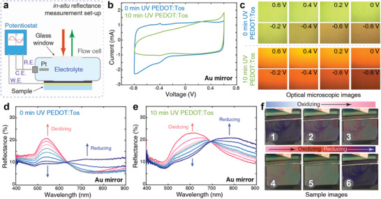
Electrochemical tuning of UV‐patterned PEDOT structural color devices. a) Schematic of the flow cell used for electrochemical measurements. R.E. is reference electrode, C.E. is counter electrode, and W.E. is working electrode. b) Cyclic voltammetry of UV patterned PEDOT:Tos films on 100 nm Au mirrors (0 and 10 min UV exposure). The scan rate was 100 mV s−1. c) Optical microscopy images of UV‐patterned PEDOT devices at different electrochemical bias (top: 0 min UV‐treated PEDOT, and bottom: 10 min UV‐treated PEDOT). d,e) In situ electrochemical tuning of the reflectance of 0 min UV‐treated PEDOT (d) and 10 min UV‐treated PEDOT (e) devices. The blue curves indicate negative bias (reducing the polymer) and the red curves indicate positive bias (oxidizing the polymer). The intensity of red and blue colors represents the increase in positive and negative electrochemical bias indicated by the arrows. The gray color curves indicate the zero electrochemical bias. f) Electrochemical tuning of a device with a 10 min UV‐patterned image (VPP time of 30 min).
3. Conclusion
We have demonstrated structural colors using conducting polymer nanofilms on metal mirrors and multicolor display devices fabricated via VPP combined with a single UV patterning step. The concept provides wide color gamut owing to UV‐controlled modification of both polymer permittivity and nanoscale thickness, which jointly modulates the structural coloration. Taking advantage of the electrochemically tuneable properties of the conducting polymer, the concept also offers reversibly switchable color images. We believe that the presented concept can aid the development of next‐generation electronic color labels and backlight‐free energy‐efficient displays. Future research may optimize UV patterning parameters and explore the many other polymers that can also be prepared by VPP, as well as different mirrors and nanocavity structures, to further improve color purity and electrochemical switching properties.
4. Experimental Section
Thin‐Film Deposition and Device Fabrication
PEDOT:Tos thin films were deposited via VPP in a vacuum chamber. Detailed information about the process and setup can be found in previous studies.[ 17 , 18 ] Briefly, substrates coated with precursor [or oxidant, consisting 2 g of Clevios C‐B 54 V3 (Heraeus, Germany), 2 g of tri‐block co‐polymer PEG‐PPG‐PEG (Sigma Aldrich), and 5 g of water‐free ethanol (99.7 wt%)] were introduced into a vacuum chamber filled with EDOT monomer vapor (by heating EDOT droplets at 60 °C). After certain polymerization time (30 or 60 min), post‐baking process at 70 °C for 2 min, and ethanol/DI water washing and nitrogen flow drying steps, PEDOT:Tos films can form on top of the substrates (glass or glass coated with metallic mirrors). For UV light exposure technique, the precursor (oxidant) films were placed under a UV lamp at wavelength of 405 nm and power of 20 mW cm−2 for different times. Grayscale photomasks or blank quartz photomask can be used during the exposure to create patterns or pure colors in the finally obtained PEDOT film devices. The grayscale photomasks used in the study were printed on transparent plastic films by normal office inkjet printers (RICOH, Japan). For display devices, glass coated with metallic mirrors (100 nm Au or 7 nm Au/3 nm Cr/100 nm Al deposited by thermal evaporation) were used as substrate and the size was normally 2.5 cm by 2.5 cm. Free‐standing PEDOT film transfer for glass substrates coated with Ag can be done with PEDOT:Tos films first deposited on silicon wafers and washed in a DI water bath (more details can be found in our previous study[ 18 ]). To deposit PEDOT:Tos films with different thicknesses without use of UV exposure, we increased spin‐coating speed of the precursor films or reduced polymerization time to prepare thin films (below 150 nm) and increased polymerization time or used layer‐by‐layer method to make thick films (above 200 nm).
Reflectance Spectroscopy and Optical Microscopy
Reflectance spectra of the devices were recorded by a custom‐made micro‐spectroscopy setup.[ 23 ] In brief, samples were illuminated by a 50 W halogen lamp attached to an optical microscope (Nikon Eclipse L200 N, Japan) and the reflected light was split into two parts at the camera port, one for optical microscopy imaging and the other for capturing spectra via an optical fiber (with a diameter of 100 µm) connected to a spectrometer (QePRO, Ocean Optics, USA). For all measurements, an objective lens of 10× magnification was used. Incidence‐angle‐dependent reflectance and scattering reflectance spectra were recorded by a custom‐made setup shown in Figures S13 and S15, Supporting Information, where a set of concentric wheels were used to control the angles with resolution of around 10°. The devices were placed at the rotation center of the inner wheel and the detector arm was mounted at the edge of the outer wheel, while collimated white light was incident on the devices at fixed angles. Rotating the wheels enables tuning of the incident or reflected/scattered light angles. Reflected light was collected by an optical light guide connected to a spectrometer (Andor Shamrock 303i with a Newton CCD detector). Device images were taken either by the optical microscope or a mobile phone (Huawei Mate 20).
Optical, Electrical, and Structural Characterization
Optical extinction spectra were acquired using a UV–vis‐NIR spectrometer PerkinElmer Lambda 900 in the range 2500 nm to 400 nm at steps of 1 nm. UV–vis‐NIR ellipsometry was performed using a J. A. Woollam Co. RC2 SE with 4–5 incident angles. All measurements were carried out in normal ambient at room temperature. UV‐treated PEDOT thin films were deposited on double‐side polished sapphire substrates (Prime Wafers, The Netherlands) and for each sample, at least two spots were measured. The details of measurements and data analysis can be found in previous studies.[ 17 ] Sheet resistance of the films, R s, was measured via four‐point probe method using a Signatone Pro4 S‐302 resistivity stand and a Keithley 2400 SourceMeter. Film thickness t was measured by a surface profiler (Dektak 3st Veeco) and confirmed by the thickness determined from ellipsometry. The electrical conductivity can be calculated by the formula σ = 1/(R s × t). Atomic force microscopy height and phase images were collected using a Veeco Dimension 3100 in tapping mode.
Optical Numerical Simulations
Numerical simulations of reflectance spectra, electric field distribution, and absorbed power distribution were carried out using the finite‐difference time‐domain method using the commercial software Lumerical FDTD solutions. Optical refractive index of UV‐treated PEDOT was extracted from ellipsometry measurements. UV‐treated (and non‐treated) PEDOT films on top of metallic mirrors and substrates were illuminated by a plane wave light source at normal incidence. Antisymmetric and symmetric boundaries were used for the x–y axis (in‐plane direction of PEDOT films) while perfectly matched layers were used for the z‐axis (out‐of‐plane direction of PEDOT films). Mesh size used in the simulation was typically 1 × 1 × 1 nm3. Stackrt command in Lumerical Script based on analytic transfer matrix method for multilayer stack was also used to verify the numerical simulation results.
Electrochemical Characterization
In situ electrochemical reflectance spectra were collected via a flow cell illustrated in Figure 5a. In this two‐electrode setup, the device was connected to the W.E. of an electrochemical potentiostat, while a Pt electrode was used as both R.E./C.E. The electrolyte used in the study was 1 m KCl water solution. For cyclic voltammetry, the scan rate was 100 mV s−1. For the reflectance measurements, the whole flow cell was placed into the homemade micro‐spectroscopy setup (with a glass window on the front side of the flow cell for light transmission). For each electrochemical bias, chronocoulometry was used and the spectra were collected after ≈30 s stabilization. In situ electrochemical absorption spectra were taken in an identical way in a quartz cuvette placed inside the sample holder of the UV–vis–NIR PerkinElmer spectrometer in the range 900 nm to 400 nm in steps of 2 nm.
Conflict of Interest
The authors declare no conflict of interest.
Supporting information
Supporting Information
Supplemental Video 1
Acknowledgements
The authors acknowledge financial support from the Swedish Foundation for Strategic Research (SSF), the Knut and Alice Wallenberg Foundation, the Swedish Research Council (VR), the Wenner‐Gren Foundations, and the Swedish Government Strategic Research Area in Materials Science on Functional Materials at Linköping University (Faculty Grant SFO‐Mat‐LiU No 2009 00971). M.P.J. is a Wallenberg Academy Fellow.
Chen S., Rossi S., Shanker R., Cincotti G., Gamage S., Kühne P., Stanishev V., Engquist I., Berggren M., Edberg J., Darakchieva V., Jonsson M. P., Tunable Structural Color Images by UV‐Patterned Conducting Polymer Nanofilms on Metal Surfaces. Adv. Mater. 2021, 33, 2102451. 10.1002/adma.202102451
Data Availability Statement
The data that support the findings of this study are available on request from the corresponding author. The data are not publicly available due to privacy or ethical restrictions.
References
- 1. Xiong K., Emilsson G., Maziz A., Yang X., Shao L., Jager E. W. H., Dahlin A. B., Adv. Mater. 2016, 28, 9956. [DOI] [PubMed] [Google Scholar]
- 2. Xiong K., Tordera D., Jonsson M. P., Dahlin A. B., Rep. Prog. Phys. 2019, 82, 024501. [DOI] [PubMed] [Google Scholar]
- 3. Rossi S., Jonsson M. P., J. Opt. 2020, 23, 015001. [Google Scholar]
- 4. Kats M. A., Blanchard R., Genevet P., Capasso F., Nat. Mater. 2013, 12, 20. [DOI] [PubMed] [Google Scholar]
- 5. Zhao Y., Xie Z., Gu H., Zhu C., Gu Z., Chem. Soc. Rev. 2012, 41, 3297. [DOI] [PubMed] [Google Scholar]
- 6.a) Kinoshita S., Structural Colors in the Realm of Nature, World Scientific, Singapore: 2008; [Google Scholar]; b) Parker A. R., J. Opt. A: Pure Appl. Opt. 2000, 2, R15; [Google Scholar]; c) Kats M. A., Capasso F., Laser Photonics Rev. 2016, 10, 699. [Google Scholar]
- 7. Comiskey B., Albert J. D., Yoshizawa H., Jacobson J., Nature 1998, 394, 253. [Google Scholar]
- 8. Cho S. I., Lee S. B., Acc. Chem. Res. 2008, 41, 699. [DOI] [PubMed] [Google Scholar]
- 9. Xiong K., Tordera D., Emilsson G., Olsson O., Linderhed U., Jonsson M. P., Dahlin A. B., Nano Lett. 2017, 17, 7033. [DOI] [PubMed] [Google Scholar]
- 10. Peng J., Jeong H. H., Smith M., Chikkaraddy R., Lin Q., Liang H. L., De Volder M. F. L., Vignolini S., Kar‐Narayan S., Baumberg J. J., Adv. Sci. 2020, 8, 2002419. [DOI] [PMC free article] [PubMed] [Google Scholar]
- 11. Brooke R., Edberg J., Crispin X., Berggren M., Engquist I., Jonsson M. P., Polymers 2019, 11, 267. [DOI] [PMC free article] [PubMed] [Google Scholar]
- 12. Brooke R., Edberg J., Iandolo D., Berggren M., Crispin X., Engquist I., J. Mater. Chem. C 2018, 6, 4663. [Google Scholar]
- 13.a) Fabretto M., Zuber K., Hall C., Murphy P., Griesser H. J., J. Mater. Chem. 2009, 19, 7871; [Google Scholar]; b) Argun A. A., Aubert P.‐H., Thompson B. C., Schwendeman I., Gaupp C. L., Hwang J., Pinto N. J., Tanner D. B., MacDiarmid A. G., Reynolds J. R., Chem. Mater. 2004, 16, 4401. [Google Scholar]
- 14. Elschner A., Kirchmeyer S., Lovenich W., Merker U., Reuter K., PEDOT: Principles and Applications of an Intrinsically Conductive Polymer, CRC Press, Boca Raton, FL, USA: 2010. [Google Scholar]
- 15. Edberg J., Iandolo D., Brooke R., Liu X., Musumeci C., Andreasen J. W., Simon D. T., Evans D., Engquist I., Berggren M., Adv. Funct. Mater. 2016, 26, 6950. [Google Scholar]
- 16. Chen S., Kang E. S. H., Chaharsoughi M. S., Stanishev V., Kühne P., Sun H., Wang C., Fahlman M., Fabiano S., Darakchieva V., Nat. Nanotechnol. 2020, 15, 35. [DOI] [PubMed] [Google Scholar]
- 17. Chen S., Kühne P., Stanishev V., Knight S., Brooke R., Petsagkourakis I., Crispin X., Schubert M., Darakchieva V., Jonsson M. P., J. Mater. Chem. C 2019, 7, 4350. [Google Scholar]
- 18. Chen S., Petsagkourakis I., Spampinato N., Kuang C., Liu X., Brooke R., Kang E. S. H., Fahlman M., Crispin X., Pavlopoulou E., J. Mater. Chem. A 2020, 8, 18726. [Google Scholar]
- 19. Kim N., Petsagkourakis I., Chen S., Berggren M., Crispin X., Jonsson M. P., Zozoulenko I., Conjugated Polymers: Properties, Processing, and Applications, CRC Press, Boca Raton, FL, USA: 2019. [Google Scholar]
- 20.a) Daqiqeh Rezaei S., Ho J., Wang T., Ramakrishna S., Yang J. K. W., Nano Lett. 2020, 20, 4422; [DOI] [PubMed] [Google Scholar]; b) Wang Z., Wang X., Cong S., Chen J., Sun H., Chen Z., Song G., Geng F., Chen Q., Zhao Z., Nat. Commun. 2020, 11, 302; [DOI] [PMC free article] [PubMed] [Google Scholar]; c) Yang Z., Chen Y., Zhou Y., Wang Y., Dai P., Zhu X., Duan H., Adv. Opt. Mater. 2017, 5, 1700029; [Google Scholar]; d) Williams C., Gordon G. S. D., Wilkinson T. D., Bohndiek S. E., ACS Photonics 2019, 6, 3132. [DOI] [PMC free article] [PubMed] [Google Scholar]
- 21. Winther‐Jensen B., Krebs F. C., Sol. Energy Mater. Sol. Cells 2006, 90, 123. [Google Scholar]
- 22.a) Rossi S., Jonsson M. P., J. Opt. 2021, 23, 015001; [Google Scholar]; b) Yang Z., Zhou Y., Chen Y., Wang Y., Dai P., Zhang Z., Duan H., Adv. Opt. Mater. 2016, 4, 1196. [Google Scholar]
- 23. Shanker R., Sardar S., Chen S., Gamage S., Rossi S., Jonsson M. P., Nano Lett. 2020, 20, 7243. [DOI] [PMC free article] [PubMed] [Google Scholar]
Associated Data
This section collects any data citations, data availability statements, or supplementary materials included in this article.
Supplementary Materials
Supporting Information
Supplemental Video 1
Data Availability Statement
The data that support the findings of this study are available on request from the corresponding author. The data are not publicly available due to privacy or ethical restrictions.


