Abstract
Spectroscopic photodetection plays a key role in many emerging applications such as context‐aware optical sensing, wearable biometric monitoring, and biomedical imaging. Photodetectors based on organic semiconductors open many new possibilities in this field. However, ease of processing, tailorable optoelectronic properties, and sensitivity for faint light are still significant challenges. Here, the authors report a novel concept for a tunable spectral detector by combining an innovative transmission cavity structure with organic absorbers to yield narrowband organic photodetection in the wavelength range of 400–1100 nm, fabricated in a full‐vacuum process. Benefiting from this strategy, one of the best performed narrowband organic photodetectors is achieved with a finely wavelength‐selective photoresponse (full‐width‐at‐half‐maximum of ≈40 nm), ultrahigh specific detectivity above 1014 Jones, the maximum response speed of 555 kHz, and a large dynamic range up to 168 dB. Particularly, an array of transmission cavity organic photodetectors is monolithically integrated on a small substrate to showcase a miniaturized spectrometer application, and a true proof‐of‐concept transmission spectrum measurement is successfully demonstrated. The excellent performance, the simple device fabrication as well as the possibility of high integration of this new concept challenge state‐of‐the‐art low‐noise silicon photodetectors and will mature the spectroscopic photodetection into technological realities.
Keywords: miniaturized spectrometers, organic photodetectors, transmission cavities, tunable spectra, wavelength selectivity
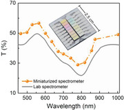
A new concept of innovative transmission cavities combined with organic photodetectors (OPDs) is proposed to achieve narrowband photodetection from the VIS to the NIR region. With this approach, an ultrahigh specific detectivity above 1014 Jones is achieved and is integrated into a miniaturized spectrometer, representing a significant step toward applying OPDs as an attractive alternative for mobile spectrometric sensing.
1. Introduction
Spectrally selective photodetection is the core demand in biomedical sensing, chemical composition, and ingredient analysis; imaging, surveillance and has also shown great potential in emerging artificial intelligence networks.[ 1 , 2 , 3 ] Commercially available spectrometers are usually made of inorganic semiconductors (mostly silicon [Si]) combined with diffraction gratings or dichroic prisms. Yet, these devices suffer from high costs as well as architectural complexity.[ 4 , 5 ] Organic photodetectors (OPDs) are emerging as promising alternatives, owing to their attractive properties such as low production costs, being lightweight, biocompatibility, and tailorable optoelectronic characteristics.[ 6 , 7 , 8 ] Significant research has been conducted mainly on polymer‐based OPDs.[ 9 , 10 , 11 , 12 ] Although small molecule‐based OPDs have received less attention, they are promising due to advantages such as facile upscaling, easy material purification, and better batch‐to‐batch reproducibility.[ 13 , 14 ]
Several strategies for color discrimination have been proposed in the literature, with two main approaches: utilization of charge collection narrowing (CCN) and optical cavity effects.[ 15 , 16 , 17 , 18 ] Despite those notable developments, several restrictions still remain for these devices. For CCN, a thick active layer (>1 µm) with appropriate optical gap and electrical transport properties is typically required.[ 19 , 20 , 21 ] Moreover, the spectral tunability of this detector concept is limited. Even though the optical cavity device concept can provide monochromatic detection over a broader wavelength range, it is still challenging to realize it in the visible spectrum.[ 22 , 23 ] Employing a very thin (nanometer‐scale) photoabsorbing layer is an approach that increases potential fabrication errors, such as short circuits and pinholes. Furthermore, the optimal detectivity has to be sacrificed by utilizing specific materials or structures with delicate optical design.[ 18 ] Therefore, advances in new device concepts are needed to improve the state‐of‐the‐art narrowband OPDs.
In this work, we propose an innovative strategy to realize tunable, narrowband, and fully vacuum‐processed OPDs by introducing a transmission cavity (TC) integrated with small‐molecule absorbers. By gradationally varying the spacer layer thickness in the TC, a continuous narrowband photoresponse from visible to the near‐infrared (NIR) spectrum (400–1100 nm) with a full‐width‐at‐half‐maximum (FWHM) of ≈40 nm is realized without changing the OPD optics. Noticeably, the optimized transmission cavity based organic photodetectors (TC‐OPDs) provide low dark current densities with large shunt resistances even when utilizing thin junctions, enabling an impressive specific detectivity (D *) over 1014 Jones and a large dynamic range (DR) up to 168 dB. Additionally, −3 dB cut‐off frequencies of 555 and 278 kHz in the visible and NIR regions are also demonstrated. As an application example, a prototype miniaturized spectrometer consisting of numerous TC‐OPDs is successfully constructed on a single substrate. It delivers signals comparable to commercial laboratory spectrometers, proving the excellent performance of our novel technology.
2. Results
A scheme of the TC‐OPD device architecture is shown in Figure 1a. Details on the layer sequence are provided in Table S1, Supporting Information. The TC is formed by a spacer inserted between two semi‐transparent Ag mirrors.[ 24 , 25 , 26 ] Here, the resonance wavelength of the cavity, equivalent to the transmission peak, is defined by the spacer layer thickness, while the cavity strength and the FWHM of the transmission spectrum are finely tuned by the semi‐transparent mirrors, enabling the manipulation of the transmission resolution. In this new concept, the TC reflects incoming photons outside of the targeted resonance wavelength peak while keeping the optimized optoelectronic structure of the OPD unchanged. A simple variation of the spacer layer thickness in the TC and a combination with the appropriate donor–acceptor system allow for tunable narrowband photodetection. To demonstrate this approach, BPhen is implemented as the spacer, whereas DCV5T‐Me:C60, BDP‐OMe:C60, and QM1:C60 are utilized as the active blend, respectively.[ 27 , 28 , 29 ] The chemical structures are depicted in Figure 1b. The absorption spectra of the blends are extended to 1100 nm, thus facilitating the realization of narrowband light detection spanning from the visible to the NIR, as illustrated in Figure 1c.
Figure 1.
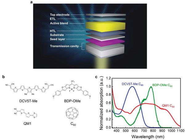
Device structure of TC‐OPDs and absorption spectra of active blends. a) Basic device structure of TC‐OPDs. HTL and ETL represent the hole‐transport layer and electron‐transport layer, respectively. Seed layers (3 nm MoO3 and 1 nm Au) are used to produce a smooth Ag mirror. b) Chemical structures of selected donor materials and the acceptor material. Buckminsterfullerenes (C60) as the acceptor, 2,2″‐((3″,4″dimethyl[2,2′:5′,2″:5″,2′″:5′″,2″″‐quinquethiophene]‐5,5″″diyl) bis(methanylylidene)) di‐malononitrile (DCV5T‐Me), CF3‐BODIPY (BDP‐OMe) and 2‐(dicyanomethylene)‐5′‐(1,3‐dithiol‐2‐ylidene)‐5,5′‐dihydro‐Delta2,2′‐bithiophene (QM1) as donors, respectively. c) Normalized absorption spectra of active blends of TC‐OPDs.
By introducing spectrally flat white light as an illumination source, the optical field distributions in TC‐OPDs are simulated via transfer‐matrix modeling (TMM),[ 30 ] as shown in Figure 2 . The optical field illustrates that the desired resonance wavelength of the TC is placed to match the position where the specific active blend absorbs a large number of photons. Since the TC is physically separated from the OPD by the intermediate glass substrate, detrimental optical interactions between the TC and the OPD, such as unwanted resonances and broadening FWHM of peaks, are avoided, allowing freely tuned narrowband photodetection. Furthermore, the simulated absorption and reflection spectra of the OPDs and TCs further demonstrate the broad spectral tunability of our devices (Figure S1, Supporting Information).
Figure 2.
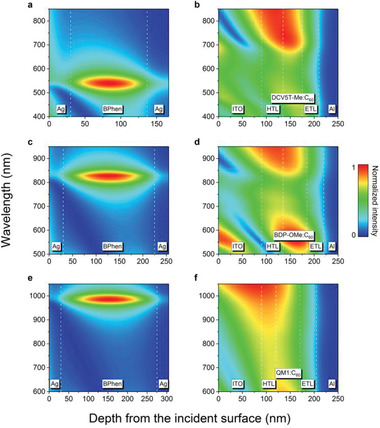
Optical field distributions of TC‐OPDs. Optical field distributions for exemplary spacer layer thicknesses of a) 107, c) 195, and e) 245 nm are shown. The TC layers have strong resonance, thus lead to high photon absorption in the related active blend of the corresponding OPD (b,d,f) at a similar wavelength. Different layer positions are marked by white dashed lines. The cathode Al thickness is 100 nm for all TC‐OPDs.
The responsivity (R) of the TC‐OPDs together with the TC transmission spectra are presented in Figure 3a–c. The peak wavelength is steadily tuned in the wavelength range from 400 to 1100 nm by varying the spacer layer thickness from 87 to 260 nm. As the TC and the OPD are optically decoupled, the peak positions in the transmission translate directly into the responsivity spectra, leading to FWHM of ≈40 nm for the TC‐OPDs (Figure S2, Supporting Information). Meanwhile, favorable responsivities of 0.17 and 0.12 A W−1 are reached in the visible and NIR region, respectively, for narrowband photodetection, corresponding to external quantum efficiencies (EQEs) of 34.1% and 19.6% (Figure S3, Supporting Information). The EQE spectra of the three OPDs without TC structure are provided in Figure S4, Supporting Information.
Figure 3.
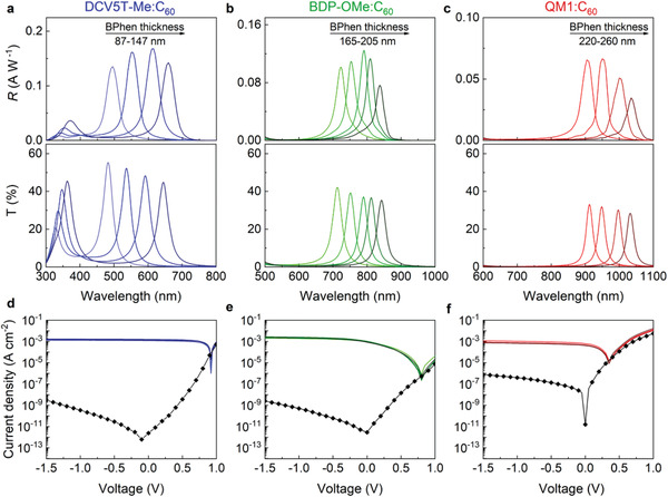
Spectral response and current density‐voltage characteristics of TC‐OPDs. Responsivity and J–V characteristics of TC‐OPDs with varied spacer (BPhen) layer thicknesses based on different active blends a,d) DCV5T‐Me:C60, b,e) BDP‐OMe:C60, and c,f) QM1:C60, respectively. Lines with and without symbols represent dark and light (100 mW cm−2 illumination) current density in J–V curves, respectively. The R sh is calculated from the slope of the J d–V curve around zero bias.
The specific detectivity, depicting the sensitivity of a photodetector to weak optical signals, is also analyzed. At zero bias, assuming that thermal noise is the primary source of noise, D * can be calculated using:
| (1) |
where R is the responsivity and A is the device area (here 6.44 mm2). The noise spectral density for thermal noise, S thermal can be expressed as:
| (2) |
in which k B is Boltzmann constant, T is temperature, and R sh is the shunt resistance. In general, low dark current is an indication of large R sh. To reduce the dark current, the excellent selectivity of p‐ and n‐ contact (BPAPF, BF‐DPB, and HATNA‐Cl6) are used, based on their low highest occupied molecular orbital and high lowest unoccupied molecular orbital, respectively. As discussed by Zheng et al., highly doped transporting layers lead to a lateral leakage current flow, which effectively increases the active area of organic diodes, thereby giving rise to a higher dark current density.[ 31 ] In order to avoid these unwanted leakage currents, the deposition of the doped layers is conducted with the aid of structured shadow masks, as suggested in the same work.[ 31 ] Additionally, the doping concentration is simultaneously optimized such that selective ohmic contacts and reduced lateral current flow are concomitantly achieved. All the organic materials used in this work are purified 2‐3 times via thermal sublimation, which is also beneficial to achieve low dark currents.[ 32 ]
The D * spectra at the detection frequency of the EQE (173 Hz) are presented in Figure 4a–c. As expected, the large R sh enables consecutive peak D * over 1014 Jones up to 810 nm. More details are listed in Table S2, Supporting Information. The maximum calculated D * of 3.0 × 10¹⁴ Jones in the visible region, together with 1.1 × 10¹⁴ Jones in the NIR region, competes well with the thick junction strategy or perovskite photodetectors and demonstrates one of the best D * of OPDs in the corresponding wavelength range, without additional gain mechanisms. Moreover, such a performance is even comparable to commercial Si photodetectors, as summarized in Figure 4d. More details are listed in Table S3, Supporting Information. To obtain the D * value with higher reliability, the actual noise level at 0 V is experimentally determined by taking Welch's method of the time‐dependent current measurements (Figure S5, Supporting Information).[ 33 , 34 ] As shown in Figure S5, Supporting Information, the noise level of our setup is ≈9 fA Hz−1/2, being larger than the thermal noise spectral density of TC‐OPDs based on active blends DCV5T‐Me:C60 and BDP OMe:C60. For these devices, the measured noise spectral densities overlap with that of the background, indicating that the actual device noise level is limited by our setup. Therefore, the calculated thermal noise provides the upper limit of D * ranging in the order of 1014 Jones. For the QM1:C60‐based TC‐OPDs, the measured noise spectral density is comparable to the theoretical value (S thermal), with a favorable D * of 4.2 × 10¹¹ Jones at 950 nm. The voltage‐dependent D * spectral profiles are also obtained from the sum of thermal and shot noise spectral density (Figure S6, Supporting Information). As found, D * decreases under reverse bias as the dark current density (J d) increases. J d scales with the total trap density and the shot‐like behavior can be attributed to the detrapping of charge carriers.[ 35 , 36 ] The relatively stable EQE values with increasing reverse bias suggest less space for further improvement of the photoresponse by promoting charge collection. This emphasizes that the J d characteristics rather than the photoresponse performance establish the limit for the detection.[ 37 ] Nevertheless, the peak D * above 1013 Jones of TC‐OPDs can still be retained under −1 V owing to their outstanding J d as shown in Figure 3d–f.
Figure 4.
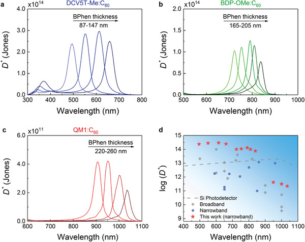
Specific detectivity spectra of TC‐OPDs and performance comparison. D * spectra of TC‐OPDs at zero bias with varied spacer (BPhen) layer thicknesses based on different active blends a) DCV5T‐Me:C60, b) BDP‐OMe:C60, and c) QM1:C60, respectively. d) Comparison of D * as a function of wavelength from previously reported photodetectors.[ 11 , 13 , 15 , 18 , 22 , 27 , 38 , 39 , 40 , 41 , 42 , 43 , 44 , 45 , 46 , 47 , 48 , 49 , 50 , 51 ] The performance values of the photodetectors from the literature are listed in Table S3, Supporting Information.
The DR quantifies the ability of the photodetector to adequately capture the variations in light intensities and is calculated via:[ 3 ]
| (3) |
where the Irr max and Irr min are the maximum and minimum light intensity, the photocurrent of the OPDs depends on the light intensity and can be fitted with a linear function in the double‐logarithmic representation. In Figure 5a, the DCV5T‐Me:C60‐based TC‐OPD photocurrent densities under varying irradiation intensity of a 505 nm light‐emitting diode (LED) are plotted, resulting in a large DR of 168 dB. For the TC‐OPDs based on BDP‐OMe:C60 and QM1:C60 active blends, DR of 164 and 136 dB are acquired under 780 and 950 nm light irradiation, respectively (Figure S7, Supporting Information), hence indicating a broad predictable photocurrent range of such devices.
Figure 5.
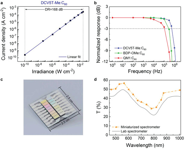
Intensity and frequency response of TC‐OPDs and miniaturized VIS‐NIR spectrometer application. a) Photoresponse of DCV5T‐Me:C60‐based TC‐OPDs for varying light intensity measured at zero bias. The device shows a DR for more than 8 orders of magnitude (168 dB). b) Normalized response loss of the TC‐OPDs versus the input signal frequency measured at zero bias. The −3 dB bandwidth is measured for the three active blends DCV5T‐Me:C60, BDP‐OMe:C60, and QM1:C60 and is specified with the black dashed line. c) Photograph of the miniaturized spectrometer application containing multiple channels of TC‐OPDs, being integrated on a single substrate with the dimension of 2.5 cm × 2.5 cm. Each detection channel reflects a separate TC‐OPD with a specific TC and OPD structure. d) Transmission spectrum of a semi‐transparent organic solar cell measured by the miniaturized spectrometer constructed in this work (orange dots) in comparison to a transmission spectrum measured by a professional laboratory spectrometer (gray solid line). Orange dots represent the peak wavelength of the corresponding TC‐OPDs; the orange dashed‐dotted line is a guide to the eye.
Furthermore, the frequency response is another critical metric for photodetectors, defining image capture speed or data acquisition rate in applications such as surveillance.[ 52 ] Figure 5b presents the −3 dB point frequency (f −3dB) of the TC‐OPDs. The QM1‐based TC‐OPD shows a f −3dB of 108 kHz, and the BDP‐OMe and DCV5T‐Me‐based TC‐OPD give a superior f −3dB = 278 and 555 kHz, respectively. Such values are sufficient for more challenging imaging applications.[ 49 ]
In contrast to the commercial optical filters, the TC structure is an effortless and cheap way to achieve light filtering with a favorable resolution and high potential for integration. To conceptually demonstrate the practical application of the TC‐OPDs, we integrate multiple devices on a small substrate (2.5 cm × 2.5 cm) to build a miniaturized spectrometer by entire vacuum processing. This easy integration is quite a big step that would be difficult to realize with commercially available optical filters. Utilizing a gradient spacer layer thickness, each pixel matches a different resonance wavelength, enabling spectroscopic photodetection with a resolution related to the FWHM of every individual photodetector. A photograph of the miniaturized spectrometer is shown in Figure 5c. To prove a sufficient spectral resolution of the integrated device for potential spectroscopic applications, the transmission spectrum of a semi‐transparent organic solar cell is measured as shown in Figure 5d.[ 53 ] Using our miniaturized spectrometer and a white light source instead of a commercial laboratory spectrometer, the transmission spectrum of the semi‐transparent organic solar cell is well reproduced. For wavelengths higher than 575 nm, a longpass filter is used to avoid current origination from the second‐order resonance of the TC. In Figure S8, Supporting Information, the transmission spectrum of the longpass filter is presented as well as the EQE of the miniaturized spectrometer.
The presented proof‐of‐concept device illustrates a combination of broad and precise spectroscopic photodetection, compactness with potential for a fast readout, plus a simple and economical fabrication method, which cannot be easily realized with other techniques. A reduction of photodetecting pixel size and glass thickness is anticipated for further miniaturization and resolution advancement of the spectrometer. In this regard, an evaporation mask with a smaller opening size is feasible, allowing the control of TC quantity during the device fabrication.
3. Conclusion
In summary, we introduce a novel concept of TC‐OPDs: the precise tailoring of the incident spectral shape is generated by the TC physics, leading to targeted photons in a narrow wavelength range absorbed by the related active blend (DCV5T‐Me:C60, BDP‐OMe:C60, and QM1:C60). In contrast to conventional methods, over 500 nm response tunability spanning from the visible to the NIR region is achieved by simply varying the spacer layer thickness, achieving large tunability without sophisticated optical design. Highly competitive performance, including low dark current, ultrahigh specific detectivity, fast response speed, and excellent DR, can be simultaneously achieved by this simple device architecture. Our approach is superior to previously reported narrowband photodetectors based on organic/perovskite materials and even challenges commercial Si‐based photodetectors as the latter lack easy spectral tunability and selectivity.
Additionally, we successfully integrate a series of TC‐OPDs on a single substrate to construct a miniaturized spectrometer and reproduce the transmission spectrum of a semi‐transparent solar cell. These promising results qualify TC‐OPDs for practical applications such as active imaging for face identification in smartphones, augmented/virtual reality goggles, and full‐weather robots.[ 47 , 54 ] This work contributes to establishing OPDs as a new technology for integrated spectroscopic sensors.
4. Experimental Section
Device Fabrication
The TC‐OPDs were fabricated by a thermal evaporation vacuum system (Kurt J. Lesker, UK) with a base pressure of less than 10−7 mbar. Before deposition, ITO substrates (Thin Film Devices, USA) were cleaned for 15 min in different ultrasonic baths with NMP solvent, deionized water, and ethanol followed by O2 plasma for 10 min. Organic materials were purified 2‐3 times via sublimation. The device stacks of all investigated TC‐OPDs are documented in Table S1, Supporting Information. A series of shadow masks and mobile shutters were utilized to control device layout and thickness variation. To produce smooth Ag mirrors, 3 nm MoO3 and 1 nm Au were used as seed layers. By adjusting the thicknesses of the BPhen layer in the TC, the photoresponse of TC‐OPDs was finely tuned. The 6.44 mm2 effective active area was defined by the geometrical overlap of the bottom and top contact. After fabrication, all devices were encapsulated by gluing a transparent glass on top of the device utilizing an epoxy resin (Nagase ChemteX XNR 5592, Japan) cured by UV light. A moisture getter (Dynic Ltd., UK) was inserted between the top contact and the glass to hinder degradation. The miniaturized spectrometer was fabricated with the device structure described above, whereas the device area amounts to 6.36 mm2.
Device Characterization
The absorption and transmission spectra were acquired with a laboratory UV–VIS–NIR spectrometer (Shimadzu SolidSpec‐3700, Japan). The EQE spectra were measured with a lock‐in amplifier (Signal Recovery SR 7265, USA) under monochromatic illumination (Oriel Xe Arc‐Lamp Apex Illuminator combined with Newport Cornerstone 260 1/4 m monochromator, USA) using a calibrated monocrystalline Si reference diode (Hamamatsu S1337, Japan, calibrated by Fraunhofer ISE). A mask was used to minimize edge effects and define an exact photoactive area (2.997 mm2). Illuminated J–V characteristics were recorded with a source‐measuring unit (SMU) (Keithley Instruments Keithley 2400, USA) under ambient conditions. Dark J–V characteristics were measured with a high‐resolution SMU (Keithley Instruments Keithley 2635, USA). Every measurement data point was acquired after the steady‐state condition was achieved. The noise spectral densities of the devices were calculated by conducting Welch's method of the time‐dependent dark currents, which were measured using an oscilloscope (Tektronix DPO7354C, USA) connected to a low noise current–voltage amplifier (Femto DLPCA‐200, Germany). The authors tried their best to optimize their measurement setup by using the aforementioned low‐noise amplifier, shortening the connection cable, as well as shielding the measurement box aiming for an accurate measurement. The DR was obtained by using three LEDs as light sources with illumination wavelength peaks at 505, 780, and 950 nm (Roithner Lasertechnik H2A1‐H505, H2A1‐H780, and H2W5‐950, Germany, respectively). The photocurrent was recorded with a high‐resolution SMU (Keithley Instruments Keithley 2635, USA) and calibrated with a Si‐photodiode. For obtaining the speed of the TC‐OPDs, three LEDs with illumination wavelength peaks at 655 (Cree‐XPEPHR‐L1‐P3‐14/15, USA), 810, and 950 nm (Roithner Lasertechnik, H2A1‐H810, and H2W5‐950, Germany) were used as light sources with an oscilloscope (Tektronix DPO7354C, USA) connected with a low noise current–voltage amplifier (Femto DLPCA‐200, Germany) to determine the time‐dependent signal.
Optical Simulation
The optical simulation was performed by using TMM. Optical constants of all layers were obtained from ellipsometry measurement.
EQE Spectra Measured with the Miniaturized Spectrometer Based on TC‐OPDs
A chopped monochromatic light (140 Hz, quartz halogen lamp [50 W] used with a Newport Cornerstone 260 1/4m monochromator, USA) was shined to the device. The current generated at the short‐circuit condition was amplified before being measured by a lock‐in amplifier (Signal Recovery 7280 DSP, USA). Light intensity was obtained by using a calibrated Si photodiode (Thorlabs FDS100‐CAL, USA). A mask was used to define an exact photoactive area (3.1 mm2).
Transmission Spectrum Measured with the Miniaturized Spectrometer Based on TC‐OPDs
A semi‐transparent organic solar cell was placed directly in front of the miniaturized spectrometer. The light of a 20 W halogen lamp was directed onto the spectrometer, and the current at zero bias was obtained by a SMU (Keithley Instruments Keithley 2450, USA). The transmission spectrum was determined from the ratio between the photocurrent measured with and without semi‐transparent organic solar cell between the light source and the spectrometer. A longpass filter (edge at ≈575 nm and the transmission spectrum is shown in Figure S8, Supporting Information) was applied in the setup to avoid the influence of the second resonance peak of BDP‐OMe‐based and QM1‐based TC‐OPDs. Each pixel of the miniaturized spectrometer had a specific peak wavelength. Therefore, narrow photoresponse peaks can be read out separately. For the transmission spectrum, the obtained transmission values for each pixel were plotted as a function of the peak wavelength of the photoresponse ratio (with and without a semi‐transparent organic solar cell) for every single pixel.
Conflict of Interest
The authors declare no conflict of interest.
Supporting information
Supporting Information
Acknowledgements
S.X., E.G., and X.J. acknowledge the financial support from China Scholarship Council (nos. 201706070125, 201706890003, and 201706140127, respectively). Moreover, the authors thank for funding through the DFG project VA 1035/5‐1 (Photogen) and the Sächsische Aufbaubank project no. 100325708 (InfraKart). Additionally, they acknowledge Louis Conrad Winkler for discussion about the noise analysis, Dr. David Wynands for discussion about the evaporation mask design and the Senorics GmbH to support the miniaturized spectrometer fabrication.
Open access funding enabled and organized by Projekt DEAL.
Xing S., Nikolis V. C., Kublitski J., Guo E., Jia X., Wang Y., Spoltore D., Vandewal K., Kleemann H., Benduhn J., Leo K., Miniaturized VIS‐NIR Spectrometers Based on Narrowband and Tunable Transmission Cavity Organic Photodetectors with Ultrahigh Specific Detectivity above 1014 Jones. Adv. Mater. 2021, 33, 2102967. 10.1002/adma.202102967
Contributor Information
Shen Xing, Email: shen.xing@tu-dresden.de.
Johannes Benduhn, Email: johannes.benduhn@tu-dresden.de.
Karl Leo, Email: karl.leo@tu-dresden.de.
Data Availability Statement
The data that support the findings of this study are available from the corresponding author upon reasonable request.
References
- 1. Xu Y., Lin Q., Appl. Phys. Rev. 2020, 7, 011315. [Google Scholar]
- 2. de Arquer F. P. G., Armin A., Meredith P., Sargent E. H., Nat. Rev. Mater. 2017, 2, 16100. [Google Scholar]
- 3. Jansen‐van Vuuren R. D., Armin A., Pandey A. K., Burn P. L., Meredith P., Adv. Mater. 2016, 28, 4766. [DOI] [PubMed] [Google Scholar]
- 4. Lukac R., J. Real‐Time Image Process. 2006, 1, 45. [Google Scholar]
- 5. Nishiwaki S., Nakamura T., Hiramoto M., Fujii T., Suzuki M.‐a., Nat. Photonics 2013, 7, 240. [Google Scholar]
- 6. Simone G., Dyson M. J., Meskers S. C., Janssen R. A., Gelinck G. H., Adv. Funct. Mater. 2019, 30, 1904205. [Google Scholar]
- 7. Sim K. M., Yoon S., Cho J., Jang M. S., Chung D. S., ACS Appl. Mater. Interfaces 2018, 10, 8405. [DOI] [PubMed] [Google Scholar]
- 8. Liu J., Wang Y., Wen H., Bao Q., Shen L., Ding L., Sol. RRL 2020, 4, 2000139. [Google Scholar]
- 9. Lin T., Wang J., Adv. Mater. 2019, 31, 1901473. [DOI] [PubMed] [Google Scholar]
- 10. Liu X., Lin Y., Liao Y., Wu J., Zheng Y., J. Mater. Chem. C 2018, 6, 3499. [Google Scholar]
- 11. Han J., Qi J., Zheng X., Wang Y., Hu L., Guo C., Wang Y., Li Y., Ma D., Qiao W., J. Mater. Chem. C 2017, 5, 159. [Google Scholar]
- 12. Wang H., Xing S., Zheng Y., Kong J., Yu J., Taylor A. D., ACS Appl. Mater. Interfaces 2018, 10, 3856. [DOI] [PubMed] [Google Scholar]
- 13. Lee C. C., Estrada R., Li Y. Z., Biring S., Al Amin N. R. A., Li M. Z., Liu S. W., Wong K. T., Adv. Opt. Mater. 2020, 8, 2000519. [Google Scholar]
- 14. Xiao L., Chen S., Chen X., Peng X., Cao Y., Zhu X., J. Mater. Chem. C 2018, 6, 3341. [Google Scholar]
- 15. Armin A., Jansen‐van Vuuren R. D., Kopidakis N., Burn P. L., Meredith P., Nat. Commun. 2015, 6, 6343. [DOI] [PubMed] [Google Scholar]
- 16. Lan Z., Lau Y. S., Wang Y., Xiao Z., Ding L., Luo D., Zhu F., Adv. Opt. Mater. 2020, 8, 2001388. [Google Scholar]
- 17. Kim S.‐K., Park S., Son H. J., Chung D. S., Macromolecules 2018, 21, 8241. [Google Scholar]
- 18. Siegmund B., Mischok A., Benduhn J., Zeika O., Ullbrich S., Nehm F., Bohm M., Spoltore D., Frob H., Korner C., Leo K., Vandewal K., Nat. Commun. 2017, 8, 15421. [DOI] [PMC free article] [PubMed] [Google Scholar]
- 19. Fang Y., Dong Q., Shao Y., Yuan Y., Huang J., Nat. Photonics 2015, 9, 679. [Google Scholar]
- 20. Shen L., Fang Y., Wei H., Yuan Y., Huang J., Adv. Mater. 2016, 28, 2043. [DOI] [PubMed] [Google Scholar]
- 21. Yazmaciyan A., Meredith P., Armin A., Adv. Opt. Mater. 2019, 7, 1801543. [Google Scholar]
- 22. Tang Z., Ma Z., Sanchez‐Diaz A., Ullbrich S., Liu Y., Siegmund B., Mischok A., Leo K., Campoy‐Quiles M., Li W., Vandewal K., Adv. Mater. 2017, 29, 1702184. [DOI] [PubMed] [Google Scholar]
- 23. Wang Y., Siegmund B., Tang Z., Ma Z., Kublitski J., Xing S., Nikolis V., Ullbrich S., Li Y., Benduhn J., Spoltore D., Vandewal K., Leo K., Adv. Opt. Mater. 2020, 9, 2001784. [Google Scholar]
- 24. Koeppe R., Müller J., Lupton J., Feldmann J., Scherf U., Lemmer U., Appl. Phys. Lett. 2003, 82, 2601. [Google Scholar]
- 25. Li Y., Tang J., Xie Z., Hung L., Lau S., Chem. Phys. Lett. 2004, 386, 128. [Google Scholar]
- 26. Lin C.‐L., Lin H.‐W., Wu C.‐C., Appl. Phys. Lett. 2005, 87, 021101. [Google Scholar]
- 27. Wang J., Ullbrich S., Hou J.‐L., Spoltore D., Wang Q., Ma Z., Tang Z., Vandewal K., ACS Photonics 2019, 6, 1393. [Google Scholar]
- 28. Li T.‐y., Meyer T., Ma Z., Benduhn J., Körner C., Zeika O., Vandewal K., Leo K., J. Am. Chem. Soc. 2017, 139, 13636. [DOI] [PubMed] [Google Scholar]
- 29. Holzmüller F., Gräßler N., Sedighi M., Müller E., Knupfer M., Zeika O., Vandewal K., Koerner C., Leo K., Org. Electron. 2017, 45, 198. [Google Scholar]
- 30. Pettersson L. A., Roman L. S., Inganäs O., J. Appl. Phys. 1999, 86, 487. [Google Scholar]
- 31. Zheng Y., Fischer A., Sergeeva N., Reineke S., Mannsfeld S. C. B., Org. Electron. 2019, 65, 82. [Google Scholar]
- 32. Drechsel J., Petrich A., Koch M., Pfützner S., Meerheim R., Scholz S., Drechsel J., Walzer K., Pfeiffer M., Leo K., SID Symp. Dig. Tech. Pap. 2006, 37, 1692. [Google Scholar]
- 33. Fang Y., Armin A., Meredith P., Huang J., Nat. Photonics 2019, 13, 1. [Google Scholar]
- 34. Konstantatos G., Clifford J., Levina L., Sargent E. H., Nat. Photonics 2007, 1, 531. [Google Scholar]
- 35. Sergeeva N., Ullbrich S., Hofacker A., Koerner C., Leo K., Phys. Rev. Appl. 2018, 9, 024039. [Google Scholar]
- 36. Kublitski J., Hofacker A., Boroujeni B. K., Benduhn J., Nikolis V. C., Kaiser C., Spoltore D., Kleemann H., Fischer A., Ellinger F., Vandewal K., Leo K., Nat. Commun. 2021, 12, 551. [DOI] [PMC free article] [PubMed] [Google Scholar]
- 37. Gielen S., Kaiser C., Verstraeten F., Kublitski J., Benduhn J., Spoltore D., Verstappen P., Maes W., Meredith P., Armin A., Adv. Mater. 2020, 32, 2003818. [DOI] [PubMed] [Google Scholar]
- 38. Liu Z.‐X., Lau T.‐K., Zhou G., Li S., Ren J., Das S. K., Xia R., Wu G., Zhu H., Lu X., Nano Energy 2019, 63, 103807. [Google Scholar]
- 39. Li W., Xu Y. L., Meng X. Y., Xiao Z., Li R. M., Jiang L., Cui L. H., Zheng M. J., Liu C., Ding L. M., Lin Q. Q., Adv. Funct. Mater. 2019, 29, 1808948. [Google Scholar]
- 40. Yeddu V., Seo G., Cruciani F., Beaujuge P. M., Kim D. Y., ACS Photonics 2019, 6, 2368. [Google Scholar]
- 41. Liu G. H., Li T. F., Zhan X. W., Wu H. B., Cao Y., ACS Appl. Mater. Interfaces 2020, 12, 17781. [DOI] [PubMed] [Google Scholar]
- 42. Liu C., Peng H., Wang K., Wei C., Wang Z., Gong X., Nano Energy 2016, 30, 27. [Google Scholar]
- 43. Xu X. F., Zhou X. B., Zhou K., Xia Y. X., Ma W., Inganas O., Adv. Funct. Mater. 2018, 28, 1805570. [Google Scholar]
- 44. Wei Y. Z., Ren Z. W., Zhang A. D., Mao P., Li H., Zhong X. H., Li W. W., Yang S. Y., Wang J. Z., Adv. Funct. Mater. 2018, 28, 1706690. [Google Scholar]
- 45. Young M., Suddard‐Bangsund J., Patrick T. J., Pajares N., Traverse C. J., Barr M. C., Lunt S. Y., Lunt R. R., Adv. Opt. Mater. 2016, 4, 1028. [Google Scholar]
- 46. Lin Q., Armin A., Lyons D. M., Burn P. L., Meredith P., Adv. Mater. 2015, 27, 2060. [DOI] [PubMed] [Google Scholar]
- 47. Xie B., Xie R., Zhang K., Yin Q., Hu Z., Yu G., Huang F., Cao Y., Nat. Commun. 2020, 11, 2871. [DOI] [PMC free article] [PubMed] [Google Scholar]
- 48. Xing S., Wang X., Guo E., Kleemann H., Leo K., ACS Appl. Mater. Interfaces 2020, 12, 13061. [DOI] [PubMed] [Google Scholar]
- 49. Lin Q., Armin A., Burn P. L., Meredith P., Nat. Photonics 2015, 9, 687. [Google Scholar]
- 50. Wang W., Zhang F., Du M., Li L., Zhang M., Wang K., Wang Y., Hu B., Fang Y., Huang J., Nano Lett. 2017, 17, 1995. [DOI] [PubMed] [Google Scholar]
- 51. Jang W., Rasool S., Kim B. G., Kim J., Yoon J., Manzhos S., Lee H. K., Jeon I., Wang D. H., Adv. Funct. Mater. 2020, 30, 2001402. [Google Scholar]
- 52. Armin A., Hambsch M., Kim I. K., Burn P. L., Meredith P., Namdas E. B., Laser Photonics Rev. 2014, 8, 924. [Google Scholar]
- 53. Jia X., Baird E. C., Blochwitz‐Nimoth J., Reineke S., Vandewal K., Spoltore D., Nano Energy 2021, 89, 106404. [Google Scholar]
- 54. Johnston M. B., Nat. Photonics 2015, 9, 634. [Google Scholar]
Associated Data
This section collects any data citations, data availability statements, or supplementary materials included in this article.
Supplementary Materials
Supporting Information
Data Availability Statement
The data that support the findings of this study are available from the corresponding author upon reasonable request.


