Abstract
An extraordinary resolution down to 50 microns is demonstrated for the first time for bulk ultrasonics, using novel micro-fabricated metamaterial lenses. The development and performance of the silicon-based Fabry–Perot type metalenses with an array of 10 micrometre square holes are discussed. Challenges in wave reception are addressed by a custom-developed micro-focal laser with a sub-micron spot size and an innovative experimental set-up together with physics based signal processing. The results provide a pathway for material diagnostics at greater depths with high resolution using micro-metalens-enhanced ultrasound as an alternative to expensive and radiation prone electromagnetic techniques.
Keywords: Sub-wavelength imaging, Micro metamaterial, Periodic holey structures, Rayleigh diffraction limitation, Acoustic microscopy
Subject terms: Mechanical engineering, Acoustics, Imaging techniques
Introduction
Evaluation of materials at greater depths with high resolution is one of the most enduring scientific challenges. Inspection and qualification of bulk components with microscopic defect features for example, is also a major challenge across critical domains including quantum materials, high energy physics, nuclear power generation, aviation, and biomedical diagnostics. Electromagnetic methods such as radiographic (X-ray) testing can achieve high resolution but with reduced penetration in solids; they typically involve ionizing radiation while also being expensive, limiting wider field application. Ultrasound can be an effective alternative with better penetration of thicker samples while being cost-effective and non-ionizing, thus allowing for the possibility of rapid and large scale online/in-situ material diagnostics. However, conventional (linear, bulk) ultrasound has limited applicability for imaging microscopic defect features due to the longer wavelengths involved1–4. Techniques such as scanning acoustic microscopy (SAM) can offer better resolution for ultrasonics at elevated frequencies on the order of 100 MHz5,6 but are restricted to the sample surface. Thus, techniques for achieving very high resolution imaging using low-frequency bulk linear ultrasonics could offer an elusive breakthrough for material diagnostics and imaging deeper inside solids.
The diffraction limit, which restricts imaging resolution to half the operating wavelength (λ/2), is linked to the exponential decay of evanescent waves that capture intricate defect details within the near field. In practical applications, the region containing evanescent wave fields typically extends to approximately one wavelength (1λ)7. Table 1 presents example values illustrating the relationship between frequency, diffraction limit, and the detectable region containing evanescent wave fields.
Table 1.
Resolution limits and detectable region containing evanescent wave field calculated for silicon wafers8.
| Probe frequency (MHz) |
Rayleigh limit ~ (λ /2), (µm) | Evanescent wave field ~ (λ) (µm) |
|---|---|---|
| 100 | 40 | 80 |
| 20 | 200 | 400 |
| 2.25 | 1777 = 1.7 mm | 3555 = 3.5 mm |
Typical approaches to overcome the diffraction limit, including near-field scanning9,10 and time reversal techniques11,12, are impacted by signal noise and complications associated with post-processing. In recent years, metamaterial lenses (henceforth referred to as “metalenses”) have been proposed for sub-wavelength resolution3,12,13 by recovering fine feature defect information from high-frequency evanescent waves7,13–15. Advancements in metalens concepts, such as the Bragg scattering superlens16,17 and the hyperlens18–21, have sparked considerable interest in overcoming the diffraction limit in both electromagnetic and acoustic wave domains. Our group has pioneered the development of macroscopic holey metalenses (see22–29 in literature) for attaining sub-wavelength resolution in the ultrasonic domain30–35.
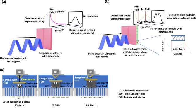
Figure 1 presents a schematic illustration of the utility of metamaterials, building upon the values in Table 1. Figure 1a presents an illustration of a line scan obtained without metalens (no resolution image plane). Figure 1b presents an illustration of a line scan obtained with metalens (resolution observed in the image plane). Also, the relationship between frequency and the detectable region (depth of penetration and evanescent wave field) is shown in Fig. 1c. However, the resolutions achievable in sub-wavelength imaging using macro-scale metamaterial ultrasonics are also typically on the scale of a few millimetres30–35. Feature dimensions in critical applications such as solid-state semiconductor/quantum components or nuclear materials, on the other hand, are typically on the micron-scale.
Fig. 1.
Schematic illustration of the utility of metamaterial: (a) Line scan obtained without metalens; (b) Line scan obtained with metalens (Inset represents Fabry Perot resonance); (c) The relationship between frequency and detectable region (evanescent wave field) within the material for commercially available probes of 100 MHz, 20 MHz, and 2.25 MHz (Arrows represent the direction of wave propagation).
In this article, we describe our efforts towards extraordinary micrometer (or ‘micron’)-scale resolution with commercial ultrasonic probes at frequencies in the range of a few MHz, using novel micro-structured metalenses aided by custom-developed sub-micron spot-size laser reception. The production of a holey metalenses with feature dimensions in the order of a few micrometres and experimental investigations in the ultrasonic regime including wave reception and signal processing are the significant challenges we addressed and overcame in this process. This paper is structured as follows, commencing with a brief explanation of the problem under study, leading into the presentation and discussion of results demonstrating a resolution of 50 microns along with quantitative analysis and discussion on the resolution limit. Following this, the “Methods” section outlines the fabrication process utilized for developing micro-metamaterials, as well as the experimental procedures involving custom-designed laser Doppler vibrometer reception. This section also presents the post-processing techniques employed to achieve the resolution.
Problem considered for the study
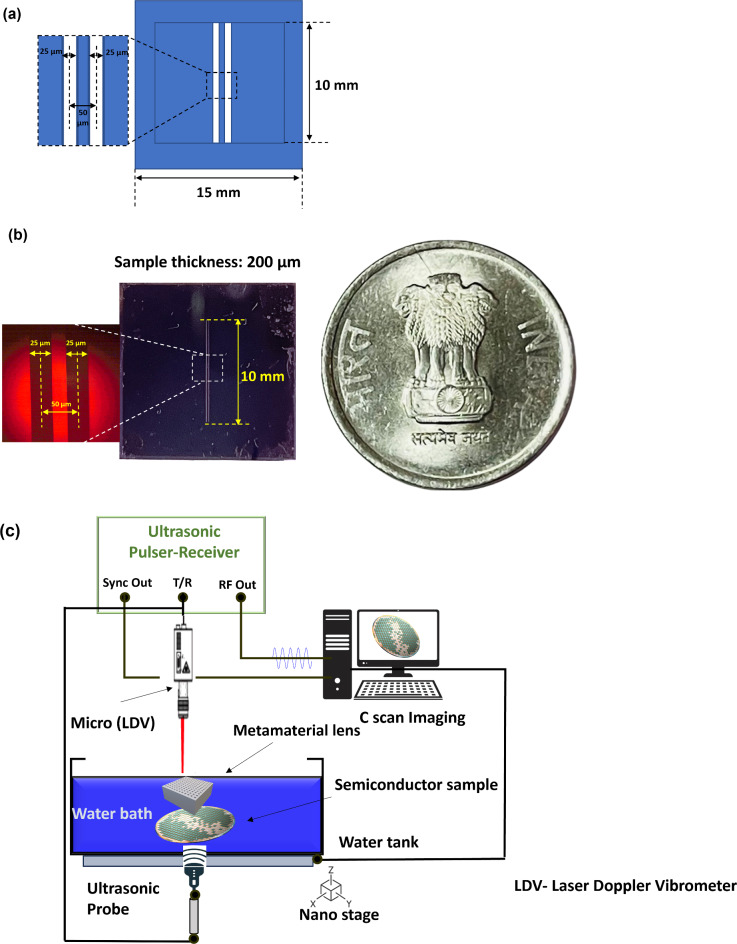
To demonstrate micron-scale resolution of defects with deep sub-wavelength feature size, we studied the problem of separating in line scans, the signatures of 2 synthetic slit-type defects having a dimension of 25 μm, with a lateral spacing of center-to-center 50 μm, in a silicon sample as depicted in Fig. 2a. Figure 2b presents optical microscope images of the slits, having a width of 25 μm and a center to center lateral distance of 50 μm. The defects were generated using deep reactive ion etching (DRIE) on 200 μm thick silicon <100> substrates. Frequently such defects or imperfections emerge within microelectronic components, integrated circuit chips, thin films, and microelectromechanical systems (MEMS) structures36.
Fig. 2.
Sample and defects studied in this paper: (a) Schematic of the slit-type defects created in a silicon wafer; (b) A photograph of the sample with defects considered for resolution demonstration (Inset is the snapshot of an optical microscopic image of the defects); (c) Schematic of the experimental setup developed by the authors for micron-scale defect characterization using linear bulk ultrasonics, as discussed in this paper.
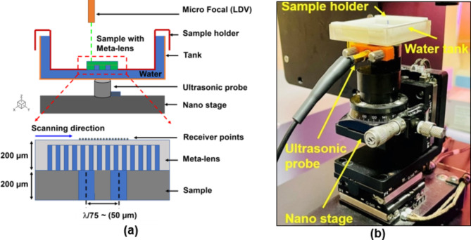
The spacing between the slit defects is smaller than the wavelength by a maximum of ~ λ/75 equivalent to 50 µm with respect to the operating frequency of 2.08 MHz in silicon. Figure 2c shows a schematic of the experimental set-up developed by the authors, for micron-scale resolution using linear bulk ultrasonic scanning in the ‘through-transmission’ mode. (A photograph of the actual experimental setup is also shown in the “Methods” section.). The proposed setup includes an ultrasonic transmitter connected to a computer-controlled nano-motion scanning stage which also hosts a tank holding the samples and the metalens for imaging. The pulser excites the transmitter, and the laser receiver detects the out-of-plane displacement from the sample and turns it into an ultrasonic signal using the receiver unit. Signals are then processed for sub-wavelength imaging.
Drawing from semiconductor fabrication methodologies and after optimising several parameters (see “Methods”), an array of micron-range straight square holes was created in a silicon base by Deep Reactive Ion Etching (DRIE). A further thin layer of gold ~ 80 nm was added on the surface of the specimen, to achieve a highly reflective condition as required for laser-based non-contact transduction we employ for receiving ultrasound. Ultrasonic inspection typically requires a water medium: however, penetration of water inside the micron-scale channels of the metalenses and maintaining their levels is a challenge. To address this, the channels of the metalenses were oxidised, making them hydrophilic after fabrication. (see “Methods” section). A micro-focal Laser Doppler Vibrometer (LDV) with a spot size < 1 micron was custom-developed to facilitate the acquisition of ultrasonic wave fields at precise spatial intervals. The laser ultrasonic receiver in this device utilizes a dual wave mixing in a photorefractive crystal, exhibiting noteworthy sensitivity and rapid response, yielding a direct correlation between its analog voltage output and the surface displacement occurring at ultrasonic frequencies. The change in surface roughness of the sample or metamaterial poses an additional challenge to keep the laser in focus. The lowest laser spot size (< 1 μm) is maintained by continuously monitoring an auxiliary output that is proportional to the optimal focusing of the laser spot. A custom-developed computer programme37 incorporates a local search algorithm that seeks the optimal auxiliary output by adjusting the height of the nano-stage manipulator and focusing the laser spot prior to acquiring the time trace (or ‘A-scan’) signal.
Through this aggregation of advancements in optimizing the micro-metalens parameters, wave reception, and imaging, we demonstrate for the first time, deep sub-wavelength resolution down to 50 microns, while operating at frequencies in the range of a few MHz.
Results
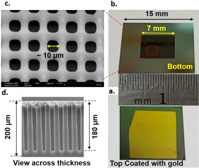
A holey structured metalens with optimised internal feature dimensions (see “Discussion”) is micro-fabricated using the standard DRIE procedure on the silicon substrate. Figure 3 presents snapshots of the fabricated micro-metalens accompanied by Scanning Electron Microscopy (SEM) images, verifying the structural integrity post-fabrication.
Fig. 3.
Photographs of micro fabricated metalens: (a) Top coated with a thin layer of gold for high reflectivity for micro-focal ultrasonic laser reception and (b) Bottom view showing metamaterial mesh with scale; and SEM images of mesh (c) Viewed from the bottom; (d) Viewed from the side.
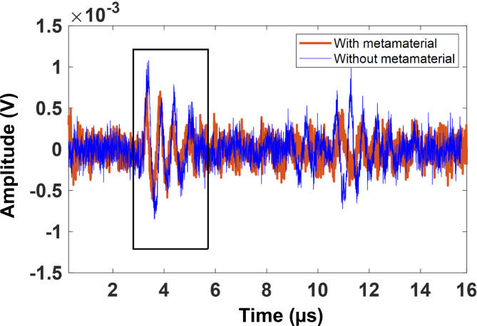
The ‘length’ (longitudinal dimension, along the wave propagation direction) of the holes in the metalens was designed in adherence to the Fabry–Perot resonance criterion of (2n − 1) ×(λ/4)38. Water was introduced into the holes as part of the experimental procedure. The microfabricated metalens effectively retains water within its cavity due to its inherent hydrophilic properties imbued via a suitable thermal oxidation process (see “Methods”). Ultrasonic waves propagate through the silicon sample, interacting with the synthetic defects, and are detected by the micro-focal LDV. The defect resolvability was validated by performing a line scan on the silicon sample both with and without the presence of a micro metalens. The ultrasonic signal in the time domain (or ‘A-scan’) for each scanning point is processed and plotted as a function of the scan length, with the first arriving ultrasonic burst appearing in a windowed format as depicted in Fig. 4.
Fig. 4.
An example time trace or ‘A-scan’ from the experiment with and without microfabricated metalens (the first arrival of the received signal is windowed for further analysis).
Post processing of experimental results demonstrating sub-wavelength resolution of micron scale
Following the post processing scheme discussed in the “Methods” section, the A-scan data for the ultrasonic inspection of 2 slits type defects spatially separated by 50 μm were analysed to demonstrate sub-wavelength resolution using the micro-metalenses proposed and fabricated as part of work reported here. The cut-off frequency of the high pass filter is chosen to leave out the low-frequency propagation modes and restore the defect-range wavelengths of the evanescent waves (see Table 2).
 |
1 |
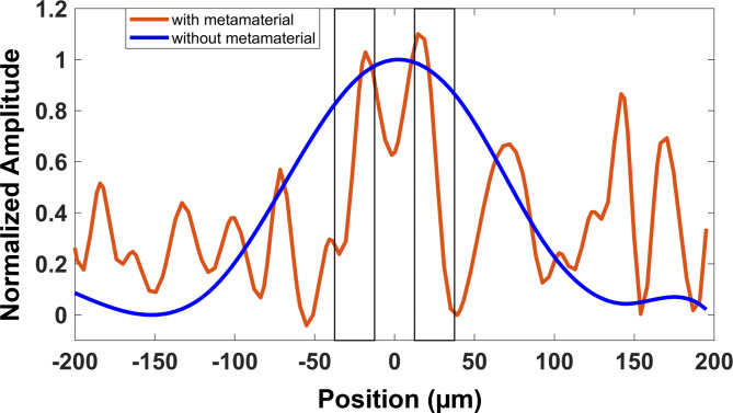
where the bulk longitudinal ultrasonic wave velocity in silicon <100> wafer is ~ 8000 m/s8, and the distance between defects in this case, is 50 μm. Figure 5 presents ‘B-Scan’ results based on post processed ultrasonic data obtained from a linear scan experiment across the sample by the LDV in spatial steps of 10 μm. To our best knowledge, these results demonstrate for the first time, defect separation resolution down to 50 μm in the bulk ultrasonic regime, facilitated by the microfabricated metalens described in this paper.
Table 2.
High-pass filter settings.
| Parameters | Value | ||
|---|---|---|---|
| Filter mode: | High-pass | ||
| Filter type: | Butterworth | ||
| Cut-off frequencies: | Defect resolution | Wavelength equivalent frequency | Chosen cut-off frequencies |
| 50 μm | 80 MHz | 60 MHz | |
Fig. 5.
‘B-scan’ results based on post processed ultrasonic data obtained from a linear scan experiment across the sample by the LDV in spatial steps of 10 μm, demonstrating a defect separation resolution down to 50 μm for the bulk ultrasonic regime achieved using the microfabricated metalens discussed in this paper (rectangular box denotes defect locations).
Quantitative analysis and resolution limit
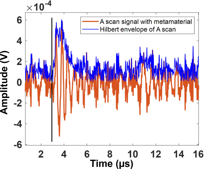
Figure 6 shows the A-scan measured in the experiments conducted with metamaterials. The wave propagates within the tank (perplex), traversing the water medium, interacting with the sub-wavelength spaced defects in the silicon sample, and emerging via the water-filled micro-metalens before propagating further through a 20 μm thick silicon substrate coated with an 80 nm layer of gold. The bulk longitudinal wave velocity in perspex, water, silicon (100) wafer, and gold film are taken as ~ 2730 m/s, ~ 1500 m/s, ~ 8000 m/s, and ~ 2210 m/s, respectively. The theoretical and experimental deviation in time of flight is given in Table 3.
Fig. 6.
A-scan obtained in experiments with for the case metamaterial, shown together with a Hilbert envelope (dashed vertical line denotes the time of arrival of the wave packet of interest).
Table 3.
Theoretical and experimental error analysis of time of flight.
| Wave path | Theoretical calculation of time of flight (Δt) in µs | Experimental observation of time of flight (Δt) in µs | Error % |
|---|---|---|---|
| 1 mm acrylic tank + 3 mm water column + 200 μm water column in slits + 180 μm water column in micro metamaterial + 20 μm in substate and 80 nm gold coating | 2.95 | 3.05 | ~ 3.3 |
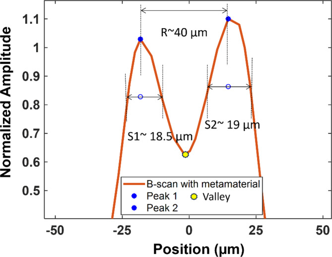
Figure 7 shows the post-processed B-scan obtained from our experiments. Table 4 lists both the anticipated and actual deviations in the size and spacing of the slits. The separation between the slits is determined by peak-to-peak measurements30–35,39, and size of S1 and S2 were calculated as half of the distance between the peak points and the minimum valley point between the resolved regions. It is important to note that while a normalized amplitude of less than 0.5*maxima is often cited as a guideline for clear differentiation between two defects or sources that are placed at a distance larger than λ/2, it is not an absolute requirement in cases where the defects are deep subwavelength. Specifically, in super-resolution imaging, this general guideline of less than 0.5* max is not always true, since the defects or sources are very closely spaced (deep subwavelength)21,27,39–42.
Fig. 7.
B scan obtained from experiments demonstrating 50 μm resolution (S1 and S2 are observed slit sizes).
Table 4.
Theoretical and experimental error analysis of B scan performance.
| Designed values (µm) | Experimental observation (µm) | Error % | |
|---|---|---|---|
| Centre to centre distance (R) | 50 | 40 | ~ 20 |
| Size of slit 1 (S1) | 25 | 18.5 | ~ 25 |
| Size of slit 2 (S2) | 25 | 19 | ~ 24 |
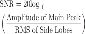
The error analysis indicates a smaller deviation in the time of flight. However, the dimensions of slit 1, slit 2, and the center-to-center distances inferred show greater variability, likely due to the limitations of our instrumentation (refer to “Discussion”). Given the precision required to maintain slit separations at 50 microns, deviations of up to 5 microns in either direction can occur. Also, we conducted a quantitative evaluation of the ‘B-scan’ profile using three key metrics: Peak-to-Side Lobe Ratio (PSLR), Signal-to-Noise Ratio (SNR), and Contrast Ratio (CR). The results are summarized in Table 5. The PSLR, which measures the distinction between the main signal peak and the largest side lobe, yielded a value of approximately 3.2 dB. This indicates that while the main peak is stronger, the side lobes still have a notable presence. The SNR, reflecting the ratio of signal strength to noise level, was about 6 dB, suggesting that the signal is clearly detectable above the noise, although the noise remains significant. Finally, the CR, which compares the amplitude in the defect region to that in the non-defect region, showed a value of around 2, indicating moderate contrast, meaning the defect is visible. Together, these metrics provide a comprehensive understanding of the signal quality, defect visibility, and the impact of noise on the B-scan profile. From this quantitative analysis we can further improve the results in our future research by overcoming limitations explained in the “Discussion” section.
Table 5.
Quantitative measurements to determine quality of B scan.
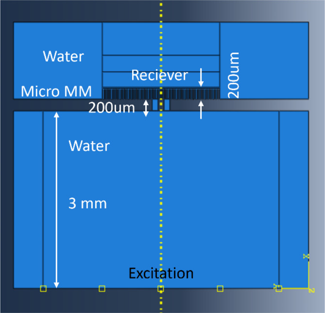
The resolution limit of our micro-metamaterial is 20 microns, corresponding to the periodicity of the micro-holes. In the metamaterial lens with a holey structure, each ‘hole’ or channel acts as a pixel, enhancing resolution by amplifying evanescent waves through Fabry–Perot resonant modes30,31. In order to shed light on this phenomenon, we conducted finite element (FE) studies and experiments to estimate the resolution limit of the micrometamaterial used in this study. The 2D FE models and problem parameters for different cases are detailed in Table 5. Our modeling approach, which closely follows previously validated methods21,30–33,42, is illustrated in Fig. 8 using a commercial FE package45. The model varies slit sizes from 100 to 20 μm and center-to-center slit spacing from 200 to 30 μm as illustrated in Table 6. Waves are generated in the model by exciting the bottom boundary in the “x” direction with acoustic pressure consisting of 3 cycle Hanning windowed tone burst signals centered at 2.08 MHz resonant frequency to demonstrate subwavelength resolution. It should be noted that 4-noded quadrilateral mesh with a seed size of 2.5 μm (which is about ~ λw/300 for 2.08 MHz in water) was used. The micro holes are modelled using the same dimensions of water columns as the experiments: 180 μm in length, 10 μm in diameter, and 20 μm of periodicity. Each holes have 4 elements to capture waves with no loss of information. The model is assigned acoustic elements with acoustic properties of water with density ρ = 1000 kg/m3 and Bulk modulus K = 2.2 GPa. Ultrasonic wave propagation in the sample is then simulated using the explicit FE algorithm provided in the commercial FE package45. Analysis was run for a total time period of 20 µs, which is sufficient for longitudinal waves to get captured as in experiments. The receiver is taken as the nodes along the horizontal line at a distance of 200 μm from the defect location, and the variation in acoustic pressure at these nodes is recorded as A-scans, as illustrated in Fig. 8. Each A-scan was post-processed to obtain B-scans. Experimental validations for Case 1 and Case 2 followed similar procedures as described in this paper, with both experimental and simulation results of B-scans. Figure 8 presents the FE model considered to find the resolution limit. These results show that resolution below the periodicity of the metalens is not achievable. Figure 9a presents both simulated and experimental B-scan results at resonant frequencies for slits spaced 200 μm apart. Figure 9b shows similar results for slits separated by 100 μm. Additionally, Fig. 9c includes simulation B-scan results for slits spaced 50 μm apart and unresolved slits measuring 20 μm in size.
Fig. 8.
Snapshot showing FE model considered for finding resolution limit.
Table 6.
Parameter studied for resolution limit.
| Center to center distance (C to C) | Size of slits (Ø) | |
|---|---|---|
| 1 | λ si (2.08 MHz)/20 (200 micro-meter) | λsi (2.08 MHz)/40 (100 micrometer) |
| 2 | λ si (2.08 MHz)/40 (100 micro-meter) | λsi (2.08 MHz)/75 (50 micro-meter) |
| 3 | λsi (2.08 MHz)/75 (50 micro-meter) | λsi (2.08 MHz)/150 (25 micro-meter) |
| 4 | λsi (2.08 MHz)/130 (30 micrometer) | λsi (2.08 MHz)/190 (20 micrometer) |
Fig. 9.
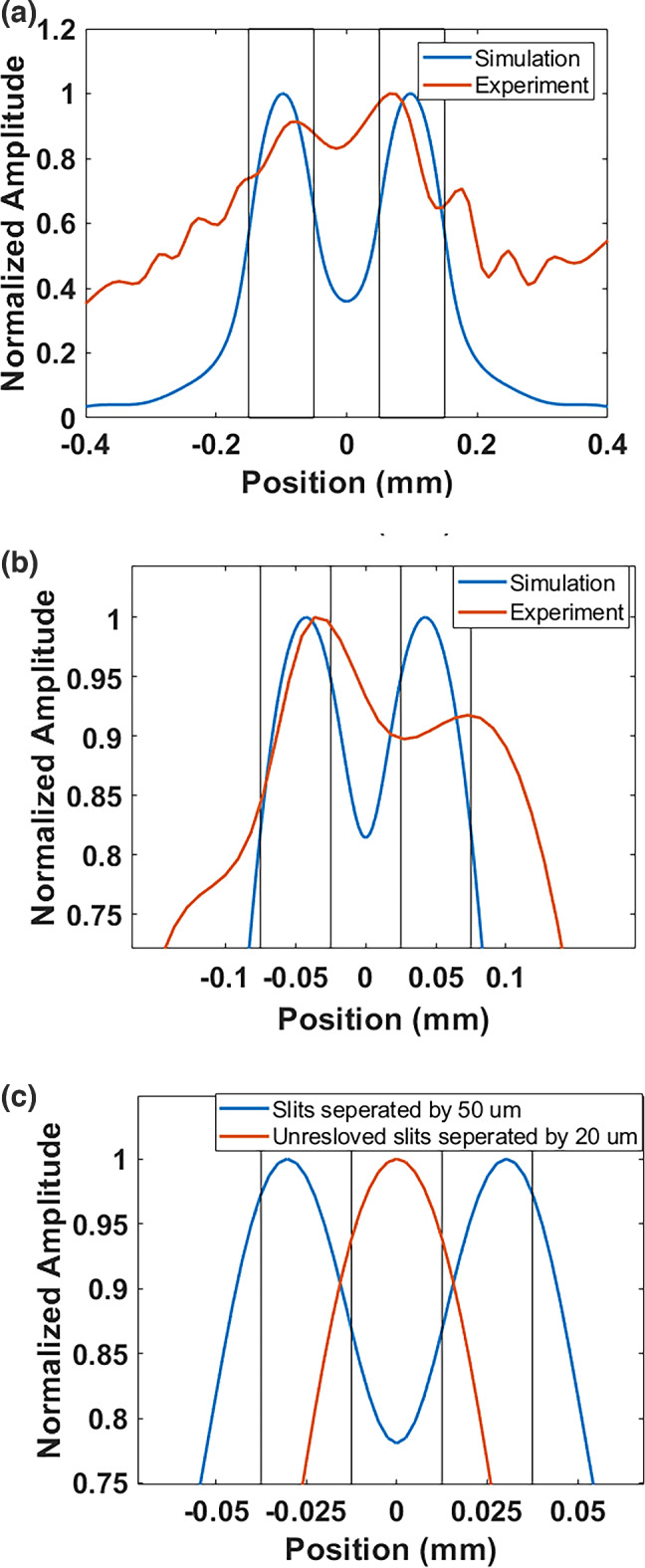
Simulation and experimental plots of amplitude across B-scans showing resolution at resonant frequencies (a) Slits are separated by 200 μm; (b) Slits are separated by 100 μm; (c) Simulation plots of amplitude across B-scan showing resolution of slits separated by 50 μm and no resolution for the slit size of 20 μm (Rectangular box denotes the slit placement).
Experimentation for demonstrating sub-wavelength resolution of micron scale
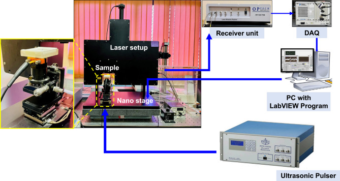
A customised experimental set-up was developed to enable experiments reported here. A sample holder and miniature water tank were fabricated using 3D printing and arranged in a configuration illustrated in Fig. 10a and shown in the photograph in Fig. 10b. The geometric characteristics of the micro-metalens, such as the hole length, width, and periodicity were carefully selected to satisfy the necessary conditions for optimal functionality, as outlined in our previous research31,38 and summarised in Table 7.
Fig. 10.
Through-transmission ultrasonic scanning of silicon sample with sub-wavelength defects by micro-focal LDV and micro-metalenses: (a) Schematic illustration (not to scale); (b) Photograph of actual experimental configuration.
Table 7.
| Optimization condition | Dimension equivalent to wavelength (λ) | Actual dimension (μm) |
|---|---|---|
| Hole length (L): (2m − 1) × (λwater/4) | ‘m’ must be integer | λwater/4 | 180 |
| Hole width (φ)λwater/ | ‘n’ must be integer & ≥ 10 | λwater/66 | 10 |
| Periodicity (Λ): 2λwater/ | ‘Λ’ must be even multiples of λ/n | 2 × (λwater/66) | 20 |
The 2.25 MHz longitudinal ultrasonic transducer, as depicted in Fig. 10b, has a diameter of 10 mm. It was excited with a 3 cycle Hanning windowed tone burst signal using an ultrasonic pulser specifically tuned to a wideband signal supporting the 1st Fabry–Perot (see “Discussion”). The wave propagates within the tank, traversing the water medium, interacting with the sub-wavelength spaced defects in the silicon sample and emerging via the water-filled micro-metalens. The wavefield then propagates further through a 20 μm thick silicon substrate coated with an 80 nm layer of gold for enhanced reflectivity enabling measurements by the micro-focal LDV. The time domain analog voltage output of the laser ultrasonic receiver unit is acquired in synchrony using a data acquisition (DAQ) card, which is connected to a computer.
A program in37 was scripted to regulate the scanning procedure, storing the A-scan signal for each reception point. Several experiments were undertaken to enhance reception and optimize the ultrasonic transmitter and receiver parameters. As the sample surface is not completely orthogonal to the micron scale beam, the LDV loses focus when it is moved during scanning. This was resolved by adding an auto-focusing algorithm to the37 code controlling the nano-stage manipulators. The Laser spot focus is maintained via continuously monitoring the auxiliary output that is optimal for the focusing of the laser. The main program created using37 incorporates a local search algorithm that seeks out the optimal value of the auxiliary output by adjusting the vertical axis of the nano stage manipulator and focusing the laser spot prior to acquiring the time domain A-scan signal.
Discussion
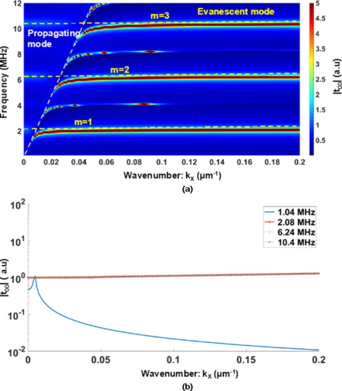
The dimensions of the holey-structured metalens were meticulously optimized to achieve a transmission coefficient with a modulus of unity for a wide range of wave vectors, encompassing both propagating and evanescent wave modes. They were also verified by plotting the dispersion signatures (see Fig. 11) obtained for a squared holey structure having holes of width (α) equal to 10 μm, periodicity (∧) equal to 20 μm, and length of 180 μm obtained for the zero-order transmission coefficient for an elastic plane wave of parallel momentum  written as Eq. (2)27:
 |
2 |
where  38;
38;  is the wave vector of the propagating fundamental waveguide mode;
  ; and
; and  .
.
Fig. 11.
Dispersion relation: (a) Modulus of transmission coefficient versus parallel momentum (x-axis) and frequency (y-axis). At the Fabry–Perot resonance modes (m = 1,2,3). The flatness of the dispersion curves can clearly be observed; (b) Modulus of zero-order transmission coefficient evaluated for 3 different frequencies; The first corresponds to the half of the 1st Fabry–Perot resonant frequency and the remaining three correspond to the three lowest Fabry–Perot resonant frequencies (m = 1,2,3).
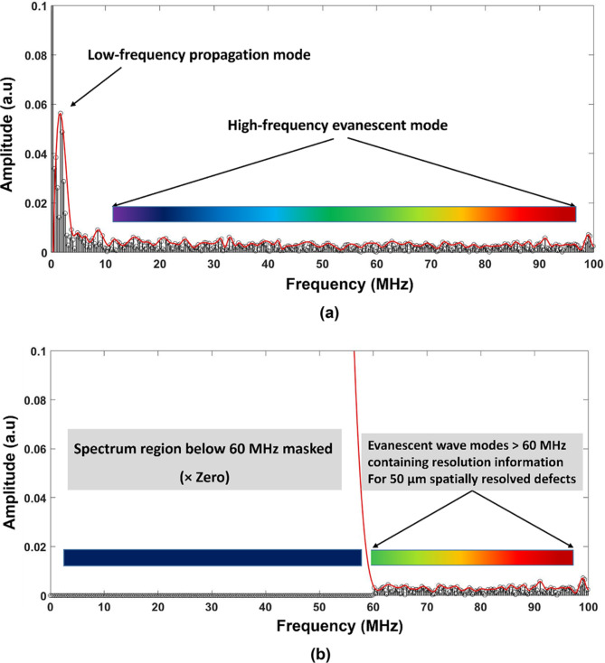
High frequency wave components scattered by the defects are transmitted to the image plane by metalenses30–34. We post-processed the received ultrasonic A-scan data by filtering out the propagating modes (and retaining the evanescent modes) through masking them in the frequency domain (see “Methods” for details). The high frequency evanescent components are recovered in the time domain by performing an inverse Fourier transform of the masked frequency spectrum. The low frequency masked spectrums of the A-scan belonging to the 50 μm spatially resolved defects in Fig. 5 are shown in Fig. 12a and b.
Fig. 12.
Processed spectrums of an arbitrary A-scan taken from 50 μm spatially resolved: (a) Without masking propagating modes; (b) With masking propagating modes.
The work reported in this contribution leverages the capabilities of low-frequency ultrasound in conjunction with microfabricated holey metamaterials, demonstrating significant promise for applications demanding fine imaging capabilities. The interaction between ultrasound and the micro-structured metamaterial yields micron-scale resolution, rendering it particularly effective for detailed, in situ analysis of electronic materials and devices, such as integrated circuits (ICs) and microelectromechanical systems (MEMS). Moreover, the versatility of this imaging technique extends beyond electronics. It holds substantial potential in the fields of Non-Destructive Evaluation (NDE) and biomedical imaging, where imaging complex structures with high resolution are crucial. These underscore the broad applicability and significant impact of our research in both industrial and medical contexts. Also recognizing the limitations of our technique is crucial for understanding its practical application and guiding future improvements. A significant limitation of this technique is the requirement for a highly polished or reflective back-wall, due to our use of a micro-focal laser vibrometer, which requires a highly ultrasonically reflective surface. Additionally, the technique is similar to other micron-scale imaging methods such as SEM and TEM, where the dimensions of samples under inspection are in the order of a few millimeters. Currently, our method is restricted to a scanning area of 2 mm by 2 mm, constrained by the capabilities of the motion stage. Additionally, the time efficiency of the process is a concern, as it takes about 6 h to perform a 1 mm B-scan. Operational challenges also include maintaining a precise water level within the microscale channels to ensure effective resonance and the need for an optimal coating on the micro-metamaterial surface to boost the laser’s sensitivity. These conditions restrict spatial movement to 10 microns per 1 mm scan. Our further work addresses these limitations, through technical improvements and optimized experimental setups to expand the method’s applicability and efficiency.
Conclusion
This paper experimentally demonstrated the development and application of a microfabricated metalens, to achieve an extraordinary resolution of ~ λ/75 down to 50 μm utilizing a 2.25 MHz commercially available bulk ultrasonic transducer. We described how this result was achieved, overcoming challenges in the fabrication of the micro-metalens and micro-focal laser reception, as well as in experimentation and signal analysis. Achieving such fine resolution at bulk ultrasonic frequencies makes this novel approach attractive for practical inspections, allowing a potential route to inspect finer features deep inside materials, thus matching the capabilities of electromagnetic techniques. The concept discussed here is protected by a provisional filing with the Indian Patent Office, titled ‘A system and method for micro-metalens based super resolution imaging using bulk ultrasonics’ with Application Number 202441010799 and filed on 15/02/2024.
Methods
Fabrication of micro-metalens
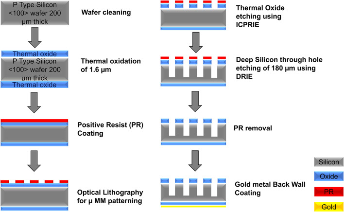
To attain an inspection resolution at the micron scale within the ultrasonic regime, the geometric characteristics of the holey-structured metamaterial must be on the order of a few micrometres. For fabricating the micro-metalens, we considered (200 μm thick) <100> silicon(si) wafers processed by dry etching. A schematic representation of the procedure for manufacturing an array of square holes with a periodicity of 10 μm in the Si wafer is given in Fig. 13. The process involves eight (8) steps. The Si wafer is first subjected to an extensive wet cleaning process using organic chemicals and acids. This is carried out to remove the stain, oil contaminants, and dust particles on the sample/substrate. In order to realize the holey-structured metamaterial, a thick masked layer with a thickness of 1.6 μm is needed above the substrate. In our case, Silicon Dioxide is used as the masking layer using a high temperature thermal oxidation furnace operating at 1100 °C. Pure oxygen is flown into the furnace, which reacts with the Si substrate, and thick Silicon dioxide is grown. The metamaterial patterns originally written in a chrome emulsion glass plate using a mask writer are then transferred to the substrate using a process called photolithography. The photosensitive polymer (Photo resistive) coated substrate is shined by a UV light, and the light exposed areas on the substrate are developed using a developer solution, thereby transferring the patterns of 10 μm hole dimensions. To remove the SiO2 (mask layer) on the developed patterns, Inductively Coupled Plasma Reactive Ion Etching (ICPRIE) technique is used. A combination of gases reacts on the exposed masked layer (SiO2) layer in a closed chamber, etches it completely till the Si layer is reached. This exposed Si hole array patterns are then subjected to deep etching technique to a depth of 180 μm using a Deep Reactive Ion Etching (DRIE) tool and a perfect vertical side wall etched deep trenches are realized. Throughout this etching process, the unexposed SiO2 layer acts as the masking layer, thereby etching only the array holes. Finally, a total of 20 μm remains as the back wall thickness on which a thin layer of 80 nm of Gold is coated using an electron beam evaporation technique.
Fig. 13.
Process flow for fabrication of micro-metalens (Note: dimensions are not to scale).
Following several iterations, the successful production of micro-metalenses featuring hole dimensions of 10 μm was achieved through the optimization of the pertinent process parameters. The fabricated samples were verified through SEM (see Fig. 3).
In the case of macro-scale metalens experiments (see30–34) retro-reflective tapes are typically affixed to the metalens to facilitate wave reception by a laser receiver. However, such tapes cannot be used with micro metalenses due to their higher thickness. Therefore, we sought to achieve a reflective surface directly onto the micro-metamaterial structure: the configuration of the micro-metamaterial was modified to incorporate blind holes, leaving a ‘backwall’ of thickness 20 μm. Additionally, a thin layer of gold of ~ 80 nm was deposited by electron beam vaporization on the posterior surface of the specimen to enhance its reflective properties (see Fig. 3).
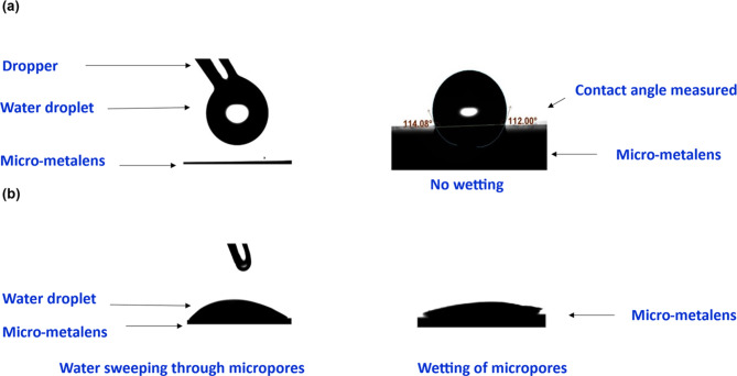
To confirm the entry of water into the micro-pores of the fabricated micro-metalens, a water droplet contact angle test was carried out using a contact angle goniometer, with results as shown in Fig. 14. In the metamaterial with hole size 10 μm, the observed contact angle was more than 90˚ which indicates a slightly hydrophobic nature of the samples (ref Fig. 14a). To eliminate this effect, the samples were thermally oxidised making them hydrophilic. Stage-wise illustrative snapshots of the water droplet spreading over the pores of the sample after oxidation during the contact angle measurement are shown in Fig. 14b.
Fig. 14.
Illustration of water droplet contact angle measurements for 10 μm holes sample: (a) Before oxidation (contact angle > 90° indicates hydrophobic nature); (b) After oxidation (sample becomes hydrophilic and water enters inside micropores).
Micro-focal ultrasonic laser Doppler vibrometer
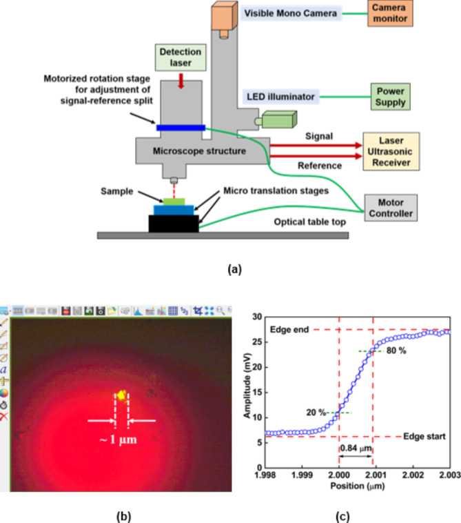
The Ultrasonic microscope detection system, (see Fig. 10a) used for experiments here was developed by the investigative team members from Intelligent Optical Systems (IOS)46. This device aims to achieve non-contact detection, utilising a high spatial resolution, to measure the displacements of a sample surface caused by ultrasonic waves generated by transducers or lasers. The system comprises a microscope assembly, a laser ultrasonic adaptive receiver/demodulator, a detection laser, and a sample positioning platform. The microscope assembly focuses the laser beam to achieve ≤ 1 μm spatial resolution on the sample surface. This is accomplished through the use of precision optical components, including lenses that optimise the trade-off between diffraction and aberration limits. The assembly includes a digital colour camera for visualisation of the laser beam and a ~ 630 nm red light emitting diode (LED) beam illuminating fiducial markings on the sample surface, and a rotation stage for optimising the power split between reference and signal interferometer arms. The operation of the adaptive receiver is based on nonlinear optical two-wave mixing in a photorefractive crystal, with high sensitivity and fast response. The receiver produces an analog voltage output, time-resolved to ~ 1 nanosec, that is proportional to the instantaneous surface displacement at ultrasonic frequencies. The continuous-wave 532-nm fiber-coupled detection laser has single longitudinal and transverse mode, with optical isolator and up to 180 mW output after coupling into PM fibre. The sample platform consists of a motorised XYZ nano-translation stage for scanning the sample and adjusting focus, with the possibility to adjust fine tip-tilt to make the sample surface normal to the optic axis by maximising the reflected signal amplitude. Figure 15a–c provide schematic illustration of the ultrasonic detection system along with camera view of the laser spot and its calculated dimensions, measured using 20–80 knife edge technique.
Fig. 15.
(a) Schematic layout of ultrasonic microscope detection system, provided by Intelligent Optical Systems. Red line represents fibre optic cables, while green line represents electrical cables; (b) Snapshot of microscopic image capture through inbuilt microscope, showing focal spot (yellow spot) of diameter < 1 μm; (c) Calculation of laser spot size using standard 20–80 knife edge width.
Experimental setup
Figure 16 presents details of the complete experimental setup. An ultrasonic transducer is firmly attached to a nano-motion scanning stage which also accommodates an acrylic tank and support structure. The sample is placed in a tank with water on top, and the micro-metalens is axially oriented right above. Ultrasound propagates vertically, traversing through the tank containing water and silicon sample wire defects. Finally the ultrasonic waves exit the system via the micro-metalens featuring a structured arrangement of microscopic holes/channels. Figure 16 also presents a photograph showcasing the experimental setup developed for sub-wavelength linear scanning using the micro-metalenses.
Fig. 16.
Schematic illustration of experimental setup for demonstrating micron-scale sub-wavelength imaging (Insert shows the photo of nano stage, sample, and probe which are explained in Fig. 10b).
A commercial ‘fingertip contact’ longitudinal ultrasonic probe (Olympus: V133-RM)47, having frequency tuned to 2.25 MHz with element size 0.25 inch was excited by an ultrasonic pulser unit (Ritec 4000 RPR)48, while the nano stage is linked to the motion controllers that are controlled by a custom written computer37 program. The micro-focal ultrasonic laser setup developed by the authors measures the spontaneous displacement caused by the ultrasonic wave field propagating out of plane from the top surface of the metalens and transmitted to the receiver unit (Optec AIR − 522-TWM)46. The DAQ (NI PXI-1033)49 unit acquires the time domain ultrasonic A-scan signal through the custom-created LabVIEW37 program. For every reception point multiple frames of A-scan signals were averaged to remove the noise and saved in a dedicated directory for post processing and analysis.
Post-processing of received A-scans for micro-metalenses based high-resolution ultrasonic imaging
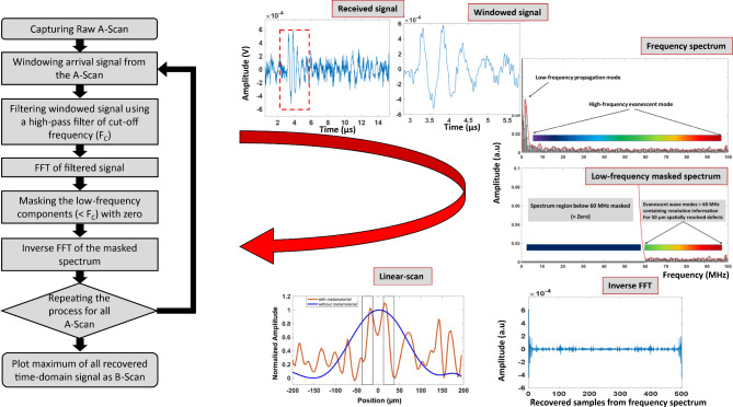
Imaging defects of spatial resolution beyond the classical Rayleigh diffraction limitation of (λ/2) is possible by extracting evanescent wave components that carry information on sub-wavelength features30–34. These evanescent waves decay exponentially within the so-called grazing or near-field region in the vicinity of the defects, and contain intricate high-frequency ultrasonic wave components having complex wavenumbers and equivalent wavelengths of the order of the defect dimension. To restore the defect-resolving information encrypted within these evanescent waves, an endoscopy mechanism is needed to translate the decaying evanescent waves without any losses to the imaging plane, where they can be captured correctly. The micro-metalens mimics an endoscope to capture and image the sub-wavelength evanescent components with microscopic resolution. The signal processing scheme used to enhance the imaging capability of the metalens, is pictorially represented through a flowchart shown in Fig. 17. The authors adopted the following process flow: The first arrival of the pulse is windowed from the A-scan, which is obtained from the receiver. The propagating components are eliminated by filtering the windowed signal up to the cut-off frequency, as indicated in Table 2. Next, from the Fast Fourier Transform (FFT), the propagating modes are suppressed using hard thresholding (zero masking). While soft thresholding could be employed with appropriate weighting by overlaying the frequency spectrum with conventional filter spectra like Butterworth and Bessel, the method we have chosen is straightforward and easier to implement. From the masked spectrum, by the inverse FFT technique the time domain signal is recovered. For every A-scan, this procedure is repeated. Finally, the B-scan profile was constructed by plotting the maximum value of the reconstructed time-domain signal against the scanning location. The reconstructed time-domain signals exclusively contain evanescent waves, preserving sub-wavelength resolution information.
Fig. 17.
Schematic illustrating the approach for post processing of the A-Scan signal captured for a metalens enhanced line scan of the silicon sample with defects.
Acknowledgements
This work was supported by the project ‘Nanoelectronics Network for Research and Applications (NNETRA)’ funded by the Indian Government Ministry of Electronics and IT (MeITy) and Department of Science & Technology (DST). The authors also gratefully acknowledge the support for Dr Prabhu Rajagopal under the National Swarnajayanti Fellowship.
Author contributions
P.R. conceived the idea. L.C. carried out simulations and experiments. L.C., C.D., M.S.S.A.A., and P.R. contributed equally to data analysis and interpretation of results. J.JD. and E.B. contributed equally to manufacturing the micro-metalens. L.C. created all the figures. L.C., M.S.S.A.A. and P.R. contributed equally to conceptualization and methodology. P.R. supervised the entire work. P.R., and E.B. contributed to sourcing the funding for this work. B.B. contributed to developing the micro focal receiver system. L.C., C.D., M.S.S.A.A. and P.R. contributed equally to writing the original draft. All the authors reviewed the manuscript.
Data availability
The data supporting this study’s findings are available from the corresponding author upon reasonable request.
Declarations
Competing interests
The authors declare no competing interests.
Footnotes
Publisher’s note
Springer Nature remains neutral with regard to jurisdictional claims in published maps and institutional affiliations.
References
- 1.Jensen, J. A. Medical ultrasound imaging. Prog. Biophys. Mol. Biol.93(1–3), 153–165 (2007). [DOI] [PubMed] [Google Scholar]
- 2.Derby, B., Briggs, G. A. D. & Wallach, E. R. Non-destructive testing and acoustic microscopy of diffusion bonds. J. Mater. Sci.18(8), 2345–2353 (1983). [Google Scholar]
- 3.Pendry, J. B. Negative refraction makes a perfect lens. Phys. Rev. Lett.85(18), 3966 (2000). [DOI] [PubMed] [Google Scholar]
- 4.Saini, A., Felice, M. V., Fan, Z. & Lane, C. J. Optimisation of the Half-Skip Total Focusing Method (HSTFM) parameters for sizing surface-breaking cracks. NDT & E Int.116(1), 102365 (2020). [Google Scholar]
- 5.Miura, K., Nasu, H. & Yamamoto, S. Scanning acoustic microscopy for characterization of neoplastic and inflammatory lesions of lymph nodes. Sci. Rep.3(1), 1255 (2013). [DOI] [PMC free article] [PubMed] [Google Scholar]
- 6.Upendran, A. & Balasubramanian, K. Identification of guided Lamb wave modes in thin metal plates using water path corrected frequency–Wavenumber [fk] analysis. NDT & E Int.139(1), 102947 (2023). [Google Scholar]
- 7.Yang, T., Jin, Y., Choi, T. Y., Dahotre, N. & Neogi, A. Mechanically tunable ultrasonic metamaterial lens with a subwavelength resolution at long working distances for bioimaging. Smart Mater. Struct.30(1), 015022 (2020). [Google Scholar]
- 8.Fromme, P., Pizzolato, M., Robyr, J. L. & Masserey, B. Lamb wave propagation in monocrystalline silicon wafers. J. Acoust. Soc. Am.143(1), 287–295 (2018). [DOI] [PubMed] [Google Scholar]
- 9.McGurn, A. & McGurn, A. Near field microscopy. Nanophotonics213(1), 445–459 (2018). [Google Scholar]
- 10.Günther, P., Fischer, U. C. & Dransfeld, K. Scanning near-field acoustic microscopy. Appl. Phys. B48(1), 89–92 (1989). [Google Scholar]
- 11.De Rosny, J. & Fink, M. Overcoming the diffraction limit in wave physics using a time-reversal mirror and a novel acoustic sink. Phys. Rev. Lett.89(12), 124301 (2002). [DOI] [PubMed] [Google Scholar]
- 12.Zhang, X. & Liu, Z. Superlenses to overcome the diffraction limit. Nat. Mater.7(6), 435–441 (2008). [DOI] [PubMed] [Google Scholar]
- 13.Lemoult, F., Fink, M. & Lerosey, G. Acoustic resonators for far-field control of sound on a subwavelength scale. Phys. Rev. Lett.107(6), 064301 (2011). [DOI] [PubMed] [Google Scholar]
- 14.Shen, Y. X. et al. Ultrasonic super-oscillation wave-packets with an acoustic meta-lens. Nat. Commun.10(1), 3411 (2019). [DOI] [PMC free article] [PubMed] [Google Scholar]
- 15.Molerón, M. & Daraio, C. Acoustic metamaterial for subwavelength edge detection. Nat. Commun.6(1), 8037 (2015). [DOI] [PMC free article] [PubMed] [Google Scholar]
- 16.Yang, X., Yin, J., Yu, G., Peng, L. & Wang, N. Acoustic superlens using Helmholtz-resonator-based metamaterials. Appl. Phys. Lett.107(19), 193505 (2015). [Google Scholar]
- 17.Jia, H. et al. Subwavelength imaging by a simple planar acoustic superlens. Appl. Phys. Lett.97(17), 173507 (2010). [Google Scholar]
- 18.Gu, Y., Cheng, Y. & Liu, X. Acoustic planar hyperlens based on anisotropic density-near-zero metamaterials. Appl. Phys. Lett.107(13), 133503 (2015). [Google Scholar]
- 19.Jacob, Z., Alekseyev, L. V. & Narimanov, E. Optical hyperlens: Far-field imaging beyond the diffraction limit. Opt. Express14(18), 8247–8256 (2006). [DOI] [PubMed] [Google Scholar]
- 20.Zhang, H., Zhou, X. & Hu, G. Shape-adaptable hyperlens for acoustic magnifying imaging. Appl. Phys. Lett.109(22), 224103 (2016). [Google Scholar]
- 21.Syed Akbar Ali, M. S. & Rajagopal, P. Far-field ultrasonic imaging using hyperlenses. Sci. Rep.12(1), 18222 (2022). [DOI] [PMC free article] [PubMed] [Google Scholar]
- 22.Liu, J., Guo, H. & Wang, T. A review of acoustic metamaterials and phononic crystals. Crystals10(4), 305 (2020). [Google Scholar]
- 23.Cheng, Y., Xu, J. Y. & Liu, X. J. One-dimensional structured ultrasonic metamaterials with simultaneously negative dynamic density and modulus. Phys. Rev.77(4), 045134 (2008). [Google Scholar]
- 24.Chen, H., Zeng, H., Ding, C., Luo, C. & Zhao, X. Double-negative acoustic metamaterial based on hollow steel tube meta-atom. J. Appl. Phys.113(10), 104902 (2013). [Google Scholar]
- 25.Ferrari, L., Lu, D., Lepage, D. & Liu, Z. Enhanced spontaneous emission inside hyperbolic metamaterials. Opt. Express22(4), 4301–4306 (2014). [DOI] [PubMed] [Google Scholar]
- 26.Lu, D. & Liu, Z. Hyperlenses and metalenses for far-field super-resolution imaging. Nat. Commun.3(1), 1205 (2012). [DOI] [PubMed] [Google Scholar]
- 27.Zhu, J. et al. A holey-structured metamaterial for acoustic deep-subwavelength imaging. Nat. Phys.7(1), 52–55 (2011). [Google Scholar]
- 28.Santra, K., Nguyen, V., Smith, E. A., Petrich, J. W. & Song, X. Localisation of nonblinking point sources using higher-order-mode detection and optical heterodyning: Developing a strategy for extending the scope of molecular, super-resolution imaging. J. Phys. Chem. B125(12), 3092–3104 (2021). [DOI] [PubMed] [Google Scholar]
- 29.Kim, H. & Rogers, E. T. Sub-wavelength annular-slit-assisted superoscillatory lens for longitudinally polarised super-resolution focusing. Sci. Rep.10(1), 1328 (2020). [DOI] [PMC free article] [PubMed] [Google Scholar]
- 30.Amireddy, K. K., Balasubramaniam, K. & Rajagopal, P. Holey-structured metamaterial lens for subwavelength resolution in ultrasonic characterisation of metallic components. Appl. Phys. Lett.108(22), 224101 (2016). [Google Scholar]
- 31.Amireddy, K. K., Balasubramaniam, K. & Rajagopal, P. Deep subwavelength ultrasonic imaging using optimised holey structured metamaterials. Sci. Rep.7(1), 7777 (2017). [DOI] [PMC free article] [PubMed] [Google Scholar]
- 32.Amireddy, K. K., Balasubramaniam, K. & Rajagopal, P. Porous metamaterials for deep sub-wavelength ultrasonic imaging. Appl. Phys. Lett.113(12), 124102 (2018). [Google Scholar]
- 33.Birir, J. K., Gatari, M. J. & Rajagopal, P. Structured channel metamaterials for deep sub-wavelength resolution in guided ultrasonics. AIP Adv.10(6), 065027 (2020). [Google Scholar]
- 34.Syed Akbar Ali, M. S., Amireddy, K. K., Balasubramaniam, K. & Rajagopal, P. Characterisation of deep sub-wavelength sized horizontal cracks using holey-structured metamaterials. Trans. Indian Inst. Met.72(11), 2917–2921 (2019). [Google Scholar]
- 35.Syed Akbar Ali, M. S., Gorthy, S. & Rajagopal, P. A device for high resolution imaging using off the shelf ultrasonic probes. Indian patent 202241049650. Provisional filed (2022)
- 36.Fisher, R. F. & Hintenlang, D. E. Micro-CT imaging of MEMS components. J. Nondestr. Eval.27(1), 115–125 (2008). [Google Scholar]
- 37.Emerson LabVIEW User Manual (2024, accessed: 15 December 2023). https://www.ni.com/docs/en-US/bundle/labview/page/user-manual-welcome.html.
- 38.Zhang, S. et al. Deep-subwavelength ultrasonic imaging by MHz column-structured metalens: First evidence of quantitative visualization of subsurface defects. Appl. Phys. Lett.123(25), 252202 (2023). [Google Scholar]
- 39.Anzan-Uz-Zaman, M., Song, K., Lee, D. G. & Hur, S. A novel approach to Fabry–Pérot-resonance-based lens and demonstrating deep-subwavelength imaging. Sci. Rep.10(1), 10769 (2020). [DOI] [PMC free article] [PubMed] [Google Scholar]
- 40.Liu, A., Zhou, X., Huang, G. & Hu, G. Super-resolution imaging by resonant tunneling in anisotropic acoustic metamaterials. J. Acoust. Soc. Am.132(4), 2800–2806 (2012). [DOI] [PubMed] [Google Scholar]
- 41.Laureti, S. et al. Trapped air metamaterial concept for ultrasonic sub-wavelength imaging in water. Sci. Rep.10(1), 10601 (2020). [DOI] [PMC free article] [PubMed] [Google Scholar]
- 42.Zul Karnain, A. A., Syed Akbar Ali, M. S., Chelat, S. K., Lopato, P. & Rajagopal, P. Near-field wave interactions with defects and their implications on sub-wavelength acoustic imaging. J. Appl. Phys.135(8), 083108 (2024). [Google Scholar]
- 43.Zhou, F., Yang, J., Jia, L., Yang, X. & Xing, M. Ultra-high resolution imaging method for distributed small satellite spotlight MIMO-SAR based on sub-aperture image fusion. Sensors21(5), 1609 (2021). [DOI] [PMC free article] [PubMed] [Google Scholar]
- 44.Lediju, M. A., Trahey, G. E., Byram, B. C. & Dahl, J. J. Short-lag spatial coherence of backscattered echoes: Imaging characteristics. IEEE Trans. Ultrason. Ferroelectr. Freq. Control58(7), 1377–1388 (2011). [DOI] [PMC free article] [PubMed] [Google Scholar]
- 45.Abaqus - Mechanical and Civil Engineering Simulation. n.d. accessed June 2 (2024). https://www.3ds.com/products-services/simulia/products/abaqus/
- 46.Intelligent Optical Systems Inc. Defect Monitoring & Inspection (2023, accessed 15 December 2023). https://intopsys.com/defect-monitoring-inspection/.
- 47.EVIDENT. Fingertip contact probe (2024, accessed 15 December 2023). https://www.olympus-ims.com/en/ultrasonic-transducers/contact-transducers/.
- 48.RITEC Inc. RPR-4000 Manual (2024, Accessed 15 December 2023). https://www.ritecinc.com/systems/.
- 49.Emerson PXI-1033 Manual (2024, accessed 15 December 2023). https://www.ni.com/en-sg/support/model.pxi-1033.html/.
Associated Data
This section collects any data citations, data availability statements, or supplementary materials included in this article.
Data Availability Statement
The data supporting this study’s findings are available from the corresponding author upon reasonable request.


