Abstract
Halide perovskite metasurfaces are attracting increasing interest for applications in light-emitting and display technologies. To access the wide range of colors required for these applications, the main mechanism exploited thus far has been chemical engineering of the perovskite compounds – this constitutes a significant limitation for the dynamic switching of optical response desirable in actual devices. Here we demonstrate polarization-dependent, dynamic control of structural color and emission wavelength in an all-dielectric phase-change halide perovskite nanograting metasurface, by temperature tuning. This is underpinned by the significant change in the perovskite optical constants which accompanies its phase-transition around room temperature. The functionalities demonstrated in our work bearing potential for applications in light-emitting devices, displays and spatial-light-modulators.
Keywords: dynamic color tuning, halide perovskite, metasurfaces, phase-change
1. Introduction
Optical metasurfaces [1], two dimensional arrays of nanostructures with subwavelength thickness which strongly confine light at the nanoscale, allow arbitrary manipulation of amplitude [2], polarization [3, 4] and phase [5] of light, enabling a variety of optical functionalities on demand [1, 6, 7]. Halide perovskites have recently emerged as a solution-processable platform of choice for the realization of all-dielectric active metasurfaces that generate a wide range of colors [8–10], produce multifold enhancement of light emission [9, 11, 12] and lasing [13–16], thanks to their outstanding luminescence properties, high refractive index, ease of processing and low cost [17, 18]. These properties make halide perovskite metasurfaces excellent candidates for applications in light-emitting diodes [19, 20], color display [8–10] and microlasers [21]. In many of these applications, however, dynamic tunability of colors is a highly desirable requirement beside the access to a wide gamut. So far, the main mechanism used to vary the color response in halide perovskites is the alteration of their chemical composition [10], an approach that is viable only for static device applications. Dynamic ion exchange approaches have also been demonstrated, but with somewhat limited applicability [22].
As a matter of fact, halide perovskites sustain a wide range of crystallographic phases [18], determined by chemical composition [23], pressure [24] and temperature [25], which can result in significant variations in the optical constants and the emission spectra [26]. While demonstrations of phase-change tunable perovskite metasurface emitters [27] and microlasers [28] have recently appeared, they operated at cryogenic temperatures (tetragonal-orthorhombic structural phase transition around 130–160 K in MAPbI3), which poses serious operational limitations – fortunately halide perovskites that experience phase transition close to room temperature have lately been discovered [29].
Here we demonstrate an all-dielectric metasurface, based on a simple nanograting design, using a halide perovskite which undergoes a phase transition around room temperature. We use the significant change in the optical constants associated to the perovskite phase transition to engineer a polarization-dependent dynamic color tunability controlled by temperature. Given the large color gamut accessible by nanostructuring, the associated color change – well distinct from that of the unstructured perovskite films – and its tunability close to room temperature, this demonstration paves the way to the realization of dynamic light-emitting devices, displays and spatial-light-modulators that could potentially operate by thermoelectric cooling.
2. Results and discussion
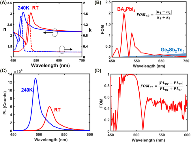
To realize the phase-change nanograting metasurface, the butylammonium lead iodide perovskite of the Ruddlesden–Popper series, BA2PbI4, was selected due to its significant change in refractive index upon phase transition near room temperature between two orthorhombic phases α n1 and β n1, respectively, at 240.5 K (α n1 → β n1) upon cooling and 270.5 (α n1 → β n1) upon heating [29]. The change in refractive index is expected to induce a change in the spectra of light reflected and transmitted by nanograting metasurface carved on BA2PbI4 films span-cast on quartz substrates, as exemplified in the schematic of Figure 1. The experimental optical constants of the BA2PbI4 films, whose thickness is estimated by atomic force microscopy (Figure S1), are retrieved by measuring their reflection and transmission spectra at the two representative temperatures of 293 and 240 K and applying Kramers–Kronig relations (Figure 2A). The agreement between the calculated and the measured reflection spectra from a BA2PbI4 film at different temperatures is illustrated in Figure S2.
Figure 1:
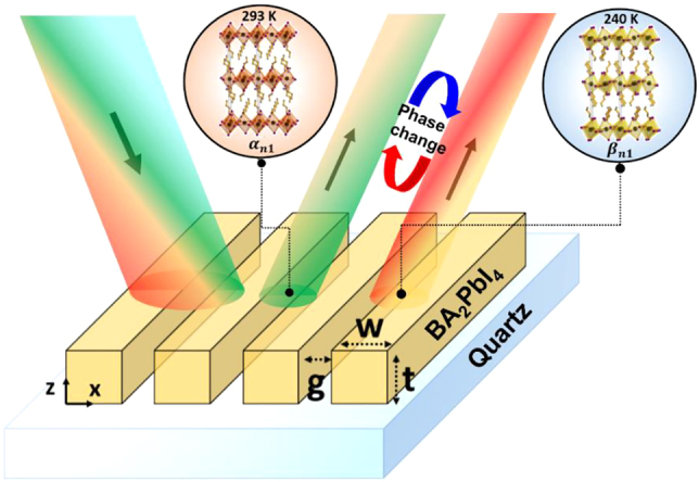
Phase-change perovskite metasurface with dynamic color tunability. Schematic of a tunable phase-change BA2PbI4 perovskite nanograting metasurface on quartz substrate. The reflected color is dynamically controlled through the switching of crystallographic phases of the perovskite by altering the ambient temperature.
Figure 2:
Optical properties and switching performances of BA2PbI4.
(A) Real n (full lines) and imaginary k (dashed lines) parts of the refractive index of BA2PbI4 at 293 K (red curves) and 240 K (blue curves). (B) Comparison between the phase-change optical constants figure of merit (FOMPC) of BA2PbI4 and Ge2Sb2Te5 in the visible spectrum. (C) Photoluminescence spectra at 293 K (red curves) and 240 K (blue curves). (D) Phase-change photoluminescence figure of merit (FOMPL) of BA2PbI4.
A phase-change figure of merit for BA2PbI4 can be defined as , where Δn denotes the change of refractive index and k 1 + k 2 is the sum of extinction coefficients of the two phases that account for optical losses [30]. The FOMPC for BA2PbI4 is higher than the FOM for the canonical phase-change chalcogenide Ge2Sb2Te5, across a significant portion of the visible spectrum, peaking at λ = 500 nm, where it outperforms by almost two order of magnitude (Figure 2B) [31].
Like the refractive index, the photoluminescence (PL) spectra of BA2PbI4 change dramatically upon phase transition: the very clear green light emission (peaking at λ = 525 nm) observed at room temperature when the film is in the α n1 phase, undergoes a substantial blueshift to become a very pure cyan (peaking at λ = 490 nm) when the film is in the β n1 phase (Figure 2C). It is possible to define a photoluminescence change figure of merit of BA2PbI4 as , which reaches 1 between 477–498 nm, corresponding to a distinct contrast between room-temperature PL and low-temperature PL.
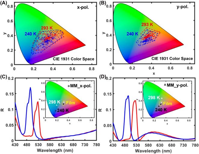
The optical response of the BA2PbI4 metasurfaces can be tailored by adjusting the nanograting parameters indicated in Figure 1, namely gap size, g, beam width, w, and milling depth, t m. This large parameter space together with the additional degree of freedom given by the anisotropy of the design, allows access to a very large color gamut. Figure 3A and B exemplify the increase in color availability brought by the nanograting metasurfaces compared to the flat film. The simulated colors reflected by the metasurfaces are shown in the CIE 1931 maps [32] for nanograting geometrical parameters varying in the following ranges: g = 50–200 nm, w = 50–350 nm and t m = 0–240 nm. A very rich reflection spectral response manifests itself in a very broad range of colors covering violet-blue to green and red for incident light with orthogonal polarizations at both room and low temperatures (the corresponding transmitted colors are shown in Figure S3).
Figure 3:
Large gamut and switching of colors with a BA2PbI4 nanograting metasurface.
(A and B) Small changes in the geometrical parameters of the nanogratings, such as gap size (g = 50–200 nm), beam width (w = 50–350 nm) and milling depth (t m = 0–240 nm) allow to access a large color gamut under, respectively, x-polarized and y-polarized incident light, thus significantly expanding on the color of the unpatterned BA2PbI4 perovskite film. (C and D) Numerically calculated reflection spectra of two BA2PbI4 perovskite metasurfaces under, respectively, x-polarized and y-polarized incident light, which show a large dynamically controllable color contrast variations of the temperature between 293 and 240 K.
Full wave electromagnetic FDTD simulations show that the optical response of the metasurfaces can be dynamically controlled with small variations in the temperature. In Figure 3C, an x-polarized plane wave, incident on a BA2PbI4 nanograting with w = 50 nm, g = 50 nm, t m = 120 nm, carved on a 240 nm thin film, induces an optical mode confined between the perovskite ridges (Figure S4A), whose spectrum is significantly blue-shifted when the temperature of the perovskite film is reduced from 293 K (red curve) to 240 K (blue curve). The corresponding color reflected by the metasurface (circles in Figure 3C inset) switches from cyan to blue while it remains of a yellow hue for the un-patterned film (squares in Figure 3C inset). Another example is shown in Figure 3D for y-polarized light incident on a nanograting with w = 150 nm, g = 50 nm, t m = 95 nm, where a similar blue-shift of the optical mode confined within the perovskite ridges (Figure S4B) takes place when the temperature is reduced from 293 to 240 K. The corresponding color reflected by the metasurface is switched from green to purple (triangles in Figure 3D inset).
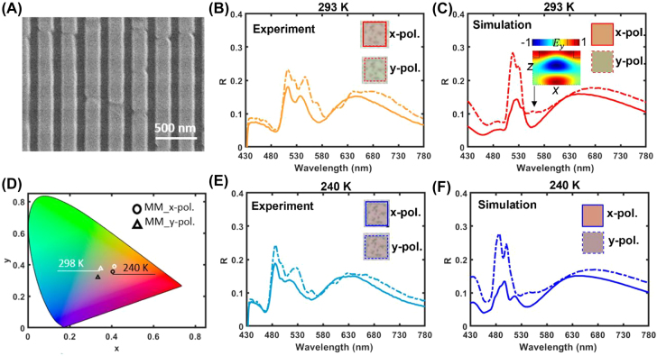
The experimental realization of a BA2PbI4 perovskite metasurface with dynamic color tunability was done by milling nanograting metasurfaces (w ∼ 220 nm, p ∼ 320 nm and t m ∼ 50 nm) in arrays of 50 × 50 μm area, through nanoimprint lithography on BA2PbI4 perovskite thin films of ∼240 nm thickness span-cast on quartz substrates (SEM image of the fabricated nanograting is shown in Figure 4A). The reflection spectra of the metasurfaces were measured under normal incidence across the entire visible region, for light polarized both parallel (y-polarized) and orthogonal (x-polarized) to the grating, at both 293 and 240 K. The subwavelength structuring of the films induced in the spectra clearly observable resonances, created by the interplay between the thin film interference and the grating modes at both room (Figure 4B) and low temperature (Figure 4E). In experiments, the color reflected by the metasurface under x-polarized light illumination barely changes through the phase transition (CCD-recorded colors in Figure 4B and E insets). However, the color reflected by the metasurface under y-polarized illumination changes from green at room temperature to cameo brown at low temperature (CCD-recorded colors in Figure 4B and E insets). Both the spectral and color response obtained via full wave electromagnetic FDTD simulations confirm the experimental observation at both room (Figure 4C) and low temperature (Figure 4F). The colors retrieved by the simulated spectra (insets of Figure 4C and F) are in good accordance with the experimental results at normal incidence. The diffraction pattern of the nanograting is expected to follow the angular dispersion of the resonances in the two polarizations, as shown by the simulated angle-resolved reflection maps in Figure S5. The more marked color change observed under y-polarized with respect to x-polarized illumination, for the fabricated metasurfaces, is confirmed by their x–y coordinate in the CIE 1931 color space (Figure 4D). The resonance excited around 540 nm under y-polarized illumination at room temperature is shown in the inset of Figure 4C; the resonance undergoes a blue shift around 530 nm when the temperature is lowered to 240 K.
Figure 4:
Experimental realization of a BA2PbI4 nanograting metasurface with dynamic color switching.
(A) SEM image of a BA2PbI4 nanograting metasurface patterned by nanoimprint lithography. (B and E) Experimental x-polarized and y-polarized reflection spectra at, respectively, 293 and 240 K. The insets show the reflected color recorded by a CCD. (D) Reconstructed reflected colors of the metasurface in the color space based on the simulated reflection spectra for both polarizations at (C) 293 K and (F) 240 K.
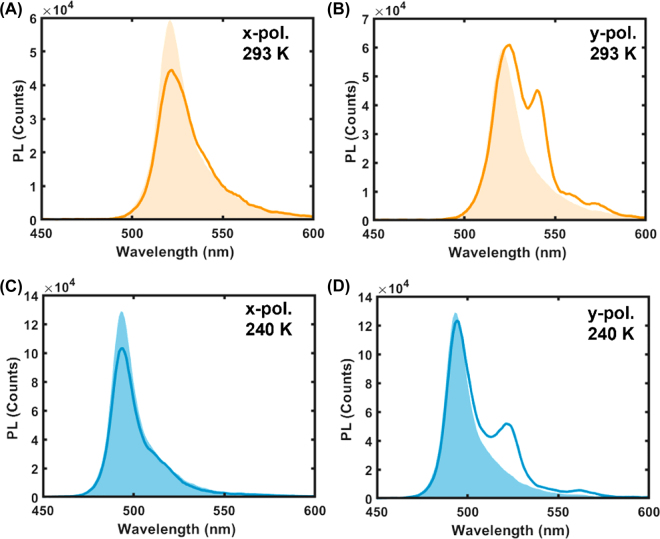
Beside the dynamic structural color tuning, the metasurface design can also be used to tune the PL emission of the perovskites. Whereas the x-polarized PL of the BA2PbI4 film (orange/blue shaded spectra in Figure 5A and C) is barely affected in intensity by structuring with a nanograting metasurface (orange and blue curves in Figure 5A and C), a distinct side peak appears in the y-polarized PL of the metasurface (orange and blue curves in Figure 5B and D). The additional peak occurs at λ = 540 nm, inducing a 4.5-fold enhancement in the PL emission at the temperature of 293 K (Figure 5B), and blue-shifts to λ = 530, associated to a 5-fold PL enhancement at 240 K nm (Figure 5D), upon phase transition of the BA2PbI4 film. This is a clear manifestation of the Purcell effect induced by the resonant mode (inset of Figure 4E) confined within the dielectric beams of the nanograting metasurface, which act as nanocavity.
Figure 5:
Polarization-dependent photoluminescence switching in BA2PbI4 nanograting metasurface upon phase transition.
(A) x-polarized and (B) y-polarized PL from the BA2PbI4 nanograting metasurface at 293 K (orange curves): the orange-shaded areas are the PL spectra from the unstructured film at the same temperature. (C) x-polarized and (D) y-polarized PL from the BA2PbI4 nanograting metasurface at 240 K (light blue curves): the blue-shaded areas are the PL spectra from the unstructured film at the same temperature.
3. Conclusions
In summary, we show that nanostructuring of perovskite films with metasurface designs, in combination with the temperature-inducing intrinsic crystallographic phase transitions, provides a simple and promising mechanism to actively control the optical response of the metasurface. By identifying a phase-change perovskite (BA2PbI4) which undergoes phase-transition and significant refractive index change around room temperature, we have experimentally realized a reconfigurable dielectric perovskite metasurface whose optical response can be tailored across a broad color gamut and achieved dynamic control of structural color and emission wavelength. With this novel approach for active tuning of the optical response of halide perovskites, beyond chemical synthesis, we expand the relatively limited library of phase change materials for the realization of active metadevices in the visible part of the spectrum. The functionalities demonstrated in our work bear potential for applications in light-emitting devices, displays and spatial-light-modulators.
4. Experimental section/methods
Perovskite film preparation : Quartz substrates are immersed in a mixture of 2 ml Hellmanex II (Hellma Analytics) and 200 ml of DI water at 353 K for 10 min, rinsed in DI water, dried under nitrogen flow and cleaned by oxygen plasma. For the synthesis of the BA2PbI4 perovskite, the following steps are followed: (i) BAI (Dyesol) and PbI2 (99.99%, TCI) powders with a molar ratio of 2:1 are added into a mixed solvent of anhydrous dimethylformamide (DMF, Sigma-Aldrich) and dimethyl sulfoxide (DMSO, Sigma-Aldrich) with a volume ratio of 3:1; (ii) the mixture is stirred for 1 h at room temperature in a N2 atmosphere to form a 0.5 M solution, followed by filtering with a poly(vinylidene fluoride) (PVDF) syringe filter (0.45 μm). The films are deposited by spin-coating the solution on the quartz substrates at 5600 rpm for 35 s while dripping toluene 5 s after starting the spinning and then annealed on a hot plate at 373 K for 15 min. The entire precursor preparation and spin coating process are processed in a N2-filled glovebox.
Thermal nanoimprint lithography: A negative resist (Hydrogen silsesquioxane, XR-1541-006) with the thickness of 170 nm is spin-coated on a silicon substrate at a speed of 1500 rpm for 1 min. E-beam lithography (ELS-7000 (Elionix Inc.)) is utilized to fabricate the nanograting metasurface under an acceleration voltage of 100 kV and the dose of 7600 μC/cm2. Inductively coupled plasma etching with a recipe of HBr (50 sccm) and O2 (3 sccm) gases at 5 mTorr is then employed to etch the Si substrate. Master molds are obtained after removing the HSQ mask in a buffered hydrofluoric acid. A nanoimprinter (Obducat NIL-60-SS-UV-Nano-imprinter) is used to transfer the metasurface from master mold to BA2PbI4 film at 30 bar and 90 °C. The imprinting time is optimized to be 30 min. At last, the imprinted sample is cooled down to room temperature and demolded from the master mold.
Numerical simulations : The reflection and transmission spectra of perovskite metasurfaces are calculated using Lumerical FDTD. Periodic boundary conditions are adopted in lateral (x, y) directions and perfectly matched layers (PML) are constructed along the incident direction (z). The reconstructed colors from the spectra are based on CIE 1931 Color Space.
Data and materials availability
The authors declare that all data supporting the findings of this study are available within this article and its supplementary material and are openly available in the NTU research data repository DR-NTU (Data) at https://doi.org/10.21979/N9/HA5YVM. Additional data related to this paper may be requested from the authors.
Supplementary Material
Supplementary Material Details
Acknowledgments
The authors acknowledge Jie Deng and Norman Soo Seng Ang for assistance with fabrication of the nanoimprint lithography mask.
Supplementary Material
The online version of this article offers supplementary material (https://doi.org/10.1515/nanoph-2022-0143).
Footnotes
Author contributions: C.S., D.C., and G.A. conceived the idea. J.T. performed numerical simulations and theoretical analysis and conducted reflection measurements. E.F. and Y.W. optimized the perovskite films. Hailong L. performed the nanoimprint lithography process under the supervision of Hong L. J.T., G.A. and C.S. drafted the manuscript. All the authors contributed to finalizing the manuscript.
Research funding: This research was supported by the A*STAR-AME programmatic fund on Nanoantenna Spatial Light Modulators for Next-Gen Display Technologies (grant A18A7b0058), and the Singapore Ministry of Education (Tier 3 grant MOE2016-T3-1-006).
Conflict of interest statement: Authors declare that they have no competing interests.
Contributor Information
Giorgio Adamo, Email: g.adamo@ntu.edu.sg.
Cesare Soci, Email: csoci@ntu.edu.sg.
References
- [1].Chen H.-T., Taylor A. J., Yu N. A review of metasurfaces: physics and applications. Rep. Prog. Phys. 2016;79:076401. doi: 10.1088/0034-4885/79/7/076401. [DOI] [PubMed] [Google Scholar]
- [2].Yang Y., Kravchenko, Briggs D. P., Valentine J. All-dielectric metasurface analogue of electromagnetically induced transparency. Nat. Commun. 2014;5:5753. doi: 10.1038/ncomms6753. [DOI] [PubMed] [Google Scholar]
- [3].Balthasar Mueller J. P., Rubin N. A., Devlin R. C., Groever B., Capasso F. Metasurface polarization optics: independent phase control of arbitrary orthogonal states of polarization. Phys. Rev. Lett. 2017;118:113901. doi: 10.1103/physrevlett.118.113901. [DOI] [PubMed] [Google Scholar]
- [4].Tian J., Adamo G., Liu H., et al. Optical Rashba effect in a light-emitting perovskite metasurface. Adv. Mater. 2022;34:2109157. doi: 10.1002/adma.202109157. [DOI] [PubMed] [Google Scholar]
- [5].Decker M., Staude I., Falkner M., et al. High-Efficiency dielectric Huygens’ surfaces. Adv. Opt. Mater. 2015;3:813–820. doi: 10.1002/adom.201400584. [DOI] [Google Scholar]
- [6].Paniagua-Domínguez R., Yu Y. F., Miroshnichenko A. E., et al. Generalized Brewster effect in dielectric metasurfaces. Nat. Commun. 2016;7:10362. doi: 10.1038/ncomms10362. [DOI] [PMC free article] [PubMed] [Google Scholar]
- [7].Li S.-Q., Xu X., Maruthiyodan Veetil R., Valuckas V., Paniagua-Domínguez R., Kuznetsov A. I. Phase-only transmissive spatial light modulator based on tunable dielectric metasurface. Science. 2019;364:1087–1090. doi: 10.1126/science.aaw6747. [DOI] [PubMed] [Google Scholar]
- [8].Gao Y., Huang C., Hao C., et al. Lead halide perovskite nanostructures for dynamic color display. ACS Nano. 2018;12:8847–8854. doi: 10.1021/acsnano.8b02425. [DOI] [PubMed] [Google Scholar]
- [9].Gholipour B., Adamo G., Cortecchia D., et al. Organometallic perovskite metasurfaces. Adv. Mater. . 2017;29:1604268. doi: 10.1002/adma.201770064. [DOI] [PubMed] [Google Scholar]
- [10].Xing G., Mathews N., Lim S. S., et al. Low-temperature solution-processed wavelength-tunable perovskites for lasing. Nat. Mater. 2014;13:476–480. doi: 10.1038/nmat3911. [DOI] [PubMed] [Google Scholar]
- [11].Makarov S. V., Milichko V., Ushakova E. V., et al. Multifold emission enhancement in nanoimprinted hybrid perovskite metasurfaces. ACS Photonics. 2017;4:728–735. doi: 10.1021/acsphotonics.6b00940. [DOI] [Google Scholar]
- [12].Adamo G., Swaha Krishnamoorthy H. N., Cortecchia D., et al. Metamaterial enhancement of metal-halide perovskite luminescence. Nano Lett. 2020;20:7906–7911. doi: 10.1021/acs.nanolett.0c02571. [DOI] [PubMed] [Google Scholar]
- [13].Chen S., Zhang C., Lee J., Han J., Nurmikko A. High-Q, low-threshold monolithic perovskite thin-film vertical-cavity lasers. Adv. Mater. 2017;29 doi: 10.1002/adma.201604781. [DOI] [PubMed] [Google Scholar]
- [14].Qin C., Sandanayaka A. S. D., Zhao C., et al. Stable room-temperature continuous-wave lasing in quasi-2D perovskite films. Nature. 2020;585:53–57. doi: 10.1038/s41586-020-2621-1. [DOI] [PubMed] [Google Scholar]
- [15].Huang C., Zhang C., Xiao S., et al. Ultrafast control of vortex microlasers. Science. 2020;367:1018–1021. doi: 10.1126/science.aba4597. [DOI] [PubMed] [Google Scholar]
- [16].Sun W., Liu Y., Qu G., et al. Lead halide perovskite vortex microlasers. Nat. Commun. 2020;11:4862. doi: 10.1038/s41467-020-18669-1. [DOI] [PMC free article] [PubMed] [Google Scholar]
- [17].Adamo G., Tian J., Krishnamoorthy H., Cortecchia D., Long G., Soci C. Halide Perovskites for Photonics . New York: AIP Publishing LLCAIP Publishing Melville; 2021. Perovskite metamaterials and metasurfaces; pp. 10–1–10–28. [Google Scholar]
- [18].Makarov S., Furasova A., Tiguntseva E., et al. Halide-perovskite resonant nanophotonics. Adv. Opt. Mater. . 2019;7:1800784. doi: 10.1002/adom.201970002. [DOI] [Google Scholar]
- [19].Wang N., Cheng L., Ge R., et al. Perovskite light-emitting diodes based on solution-processed self-organized multiple quantum wells. Nat. Photonics. 2016;10:699–704. doi: 10.1038/nphoton.2016.185. [DOI] [Google Scholar]
- [20].Lin K., Xing J., Quan L. N., et al. Perovskite light-emitting diodes with external quantum efficiency exceeding 20 per cent. Nature. 2018;562:245–248. doi: 10.1038/s41586-018-0575-3. [DOI] [PubMed] [Google Scholar]
- [21].Wang K., Wang S., Xiao S., Song Q. Recent advances in perovskite micro- and nanolasers. Adv. Opt. Mater. . 2018;6:1800278. doi: 10.1002/adom.201800278. [DOI] [Google Scholar]
- [22].Zhang C., Xiao S., Wang Y., et al. Lead halide perovskite‐based dynamic metasurfaces. Laser Photon. Rev. . 2019;13:1900079. doi: 10.1002/lpor.201970030. [DOI] [Google Scholar]
- [23].Wang Y., Quintana X., Kim J., et al. Phase segregation in inorganic mixed-halide perovskites: from phenomena to mechanisms. Photon. Res. . 2020;8:A56–A71. doi: 10.1364/prj.402411. [DOI] [Google Scholar]
- [24].Liu S., Sun S., Kwan Gan C., et al. Manipulating efficient light emission in two-dimensional perovskite crystals by pressure-induced anisotropic deformation. Sci. Adv. 2019;5:eaav9445. doi: 10.1126/sciadv.aav9445. [DOI] [PMC free article] [PubMed] [Google Scholar]
- [25].Jiang Y., Soufiani A. M., Gentle A., et al. Temperature dependent optical properties of CH3NH3PbI3 perovskite by spectroscopic ellipsometry. Appl. Phys. Lett. . 2016;108:061905. doi: 10.1063/1.4941710. [DOI] [Google Scholar]
- [26].Kong W., Ye Z., Qi Z., et al. Characterization of an abnormal photoluminescence behavior upon crystal-phase transition of perovskite CH3NH3PbI3. Phys. Chem. Chem. Phys. 2015;17:16405–16411. doi: 10.1039/c5cp02605a. [DOI] [PubMed] [Google Scholar]
- [27].Tiguntseva E. Y., Sadrieva Z., Stroganov B. V., et al. Enhanced temperature-tunable narrow-band photoluminescence from resonant perovskite nanograting. Appl. Surf. Sci. 2019;473:419–424. doi: 10.1016/j.apsusc.2018.12.084. [DOI] [Google Scholar]
- [28].Tian J., Adamo G., Liu H., et al. Phase-change Perovskite Tunable Microlaser. 2021. arXiv preprint arXiv:2107.05239. [DOI] [PubMed] [Google Scholar]
- [29].Cortecchia D., Neutzner S., Yin J., et al. Structure-controlled optical thermoresponse in Ruddlesden-Popper layered perovskites. Apl. Mater. 2018;6 doi: 10.1063/1.5045782. [DOI] [Google Scholar]
- [30].Li Y., Singh A., Krylyuk S., Davydov A., Jaramillo R. Low-Dimensional Materials and Devices 2019 . Vol. 11085. San Diego: International Society for Optics and Photonics; 2019. p. 110850T. [PMC free article] [PubMed] [Google Scholar]
- [31].Sreekanth K. V., Han S., Singh R. Ge2 Sb2 Te5 -based tunable perfect absorber cavity with phase singularity at visible frequencies. Adv. Mater. 2018;30:1706696. doi: 10.1002/adma.201706696. [DOI] [PubMed] [Google Scholar]
- [32].Fairman H. S., Brill M. H., Hemmendinger H. How the CIE 1931 color-matching functions were derived from Wright-Guild data. Color Res. Appl. 1997;22:11–23. doi: 10.1002/(sici)1520-6378(199702)22:1<11::aid-col4>3.0.co;2-7. The Colour Group (Great Britain), Canadian Society for Color, Color Science Association of Japan, Dutch Society for the Study of Color, The Swedish Colour Centre Foundation, Colour Society of Australia, Centre Français de la Couleur. [DOI] [Google Scholar]
Associated Data
This section collects any data citations, data availability statements, or supplementary materials included in this article.
Supplementary Materials
Supplementary Material Details


