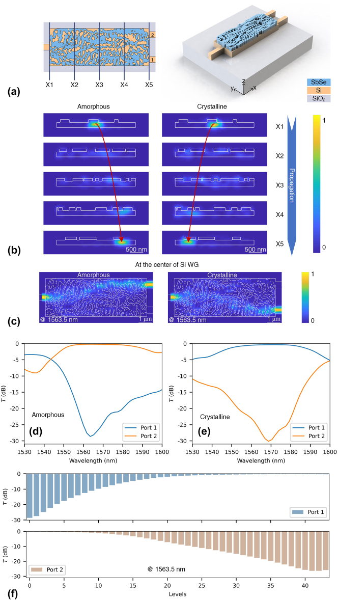
Figure 3:
The structure diagram and performance of the OS. (a) The top view of the device and the 3D schematic diagram of the OS. X1 to X5 are different positions along the propagation direction of OS with a distance to the input port of 0, 2, 4, 6, and 8 μm, respectively. (b) The energy distribution (y–z plane) of different positions of OS at amorphous and crystalline states, respectively. (c) The energy flow (x–y plane) at the center of the silicon waveguide. The simulated spectra of amorphous (d) and crystalline (e) state. (f) The simulated multi-level switching of the OS at 1563.5 nm.

