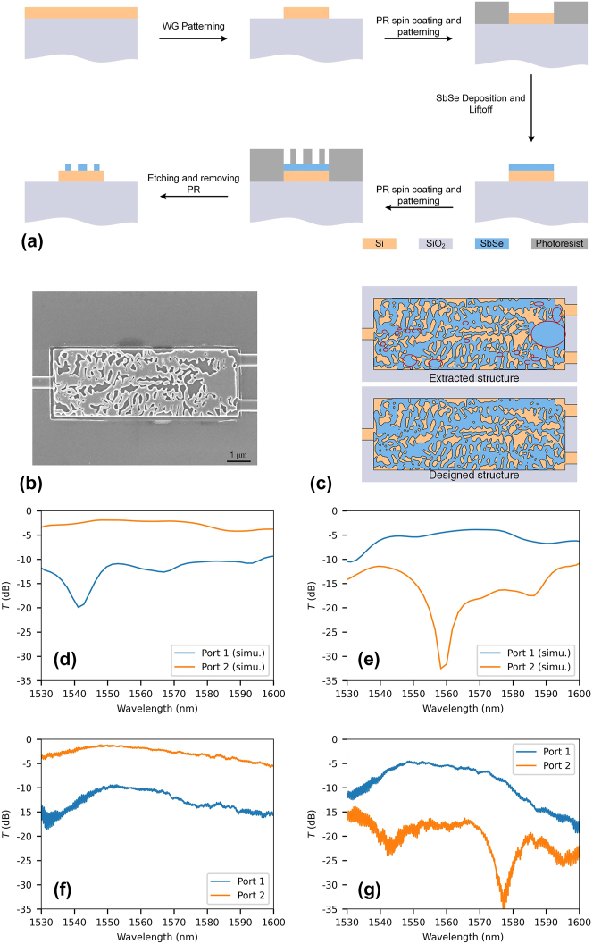
Figure 4:
The fabrication and characterization of the fabrication error-tolerant OS. (a) The flow chart for device fabrication. (b) The scanning electron microscope (SEM) image of the fabricated device. (c) Comparison of the extracted pattern with the designed structure. The section highlighted within the red circle represents the missing pattern of the fabricated device. The simulated optical response of the extracted structure at amorphous (d) and crystalline (e) states. The measured spectra of the fabricated device at amorphous (f) and crystalline (g) states.

