Abstract
Among the various two-dimensional (2D) materials, more than 99% of them are noncentrosymmetric. However, since the commonly used substrates are generally centrosymmetric, antiparallel islands are usually inevitable in the growth of noncentrosymmetric 2D materials because of the energetic equivalency of these two kinds of antiparallel islands on centrosymmetric substrates. Therefore, achieving the growth of noncentrosymmetric 2D single crystals has long been a great challenge compared with the centrosymmetric ones like graphene. In this review, we presented the remarkable efforts and progress in the past decade, through precise chemical processes. We first discussed the great challenge and possible strategies in the growth of noncentrosymmetric 2D single crystals. Then, we focused on the advancements made in producing representative noncentrosymmetric 2D single crystals, including hexagonal boron nitride (hBN), transition metal dichalcogenides (TMDs), and other noncentrosymmetric 2D materials. At last, we summarized and looked forward to future research on the growth of layer-, stacking-, and twist-controlled noncentrosymmetric 2D single crystals and their heterostructures.
Keywords: noncentrosymmetric, two-dimensional materials, single crystals, hexagonal boron nitride, transition metal dichalcogenides
1. Introduction
1.1. The Rise of Two-Dimensional (2D) Materials
2D materials are a class of materials that have a thickness of only a few atomic layers. In 2004, the first kind of 2D material, graphene, was mechanically exfoliated.1 Since then, many different kinds of 2D materials have been discovered, including hexagonal boron nitride (hBN), transition metal dichalcogenides (TMDs, such as MoSe2, MoS2, MoTe2, WSe2, WS2, ReS2, and TaS2), simple substances (such as phosphorene, silicene, and germanene), group III/V monochalcogenides (such as In2Se3, SnS, and GeSe), group III–IV binary compounds (such as GaN and GaAs), among others.
In contrast to the bulk materials, 2D materials confine electrons within a plane, leading to numerous distinctive properties and potential applications.2 These materials provide excellent platforms for fundamental scientific exploration, enabling the uncovering of intriguing physical phenomena such as room temperature quantum Hall effect, Mott insulation state, anomalous superconductivity, and fractional quantum anomalous Hall effect.3−6 Moreover, their high carrier mobility, adjustable bandgap, strong spin–valley coupling, robust light–matter interaction, large specific surface area, and short diffusion path make 2D materials highly promising candidates for next-generation electronics, optoelectronics, sensors, energy storage, catalysis, and biomedicine.7−13
1.2. Challenge in the Growth of Noncentrosymmetric 2D Single Crystals
For practical applications, achieving large 2D single crystals is a grail. The exceptional single crystallinity and absence of grain boundaries (GBs) in these crystals ensure their intrinsic physical and chemical properties, thereby guaranteeing ultimate performance and uniformity of devices. Numerous experimental studies and theoretical calculations have indicated that the presence of GBs in polycrystalline hBN and TMDs significantly restrict their electrical properties.14−17 The defects and GBs serve as charge scattering sites and traps, hindering the advancement of high-performance electronics. Specifically, GBs in hBN are associated with conductive defects localized at the Cu and hBN grain boundaries. These defects can be visually observed through conductive atomic force microscopy (AFM) imaging, which reveals the distribution of conductive defects across hBN films (Figure 1a,b).18 Such GBs in hBN are inherently susceptible to electrical breakdown, chemical attack, or mechanical failure due to their atomic stitching structure. This renders monolayer hBN films ineffective for their intended applications as ultrathin dielectrics, barrier layers, or separation membranes. Additional evidence further demonstrates the detrimental effects caused by these GBs. Ly et al. measured the electrical transport of polycrystalline MoS2 with a GB misorientation angle of 19°, the results reveal that the intradomain regions consistently exhibit higher μFE and reduced RS compared to interdomain regions.19 A similar trend is also observed in MoS2 islands with tilted boundaries (Figure 1c). Both parallel and perpendicular devices experience a decrease of 30% in on-state boundary conductance when compared to pristine crystals (Figure 1d).20 Furthermore, the susceptibility of grain boundaries to environmental degradation complicates their utilization in electronics. For instance, Wang et al. reported that GBs in MoSe2 were etched under wet H2O vapor exposure, highlighting their environmental instability.21 These findings are crucial for applications requiring materials that are stable and reliable. Therefore, great efforts have been employed on the growth of 2D single crystals in the past decade.
Figure 1.
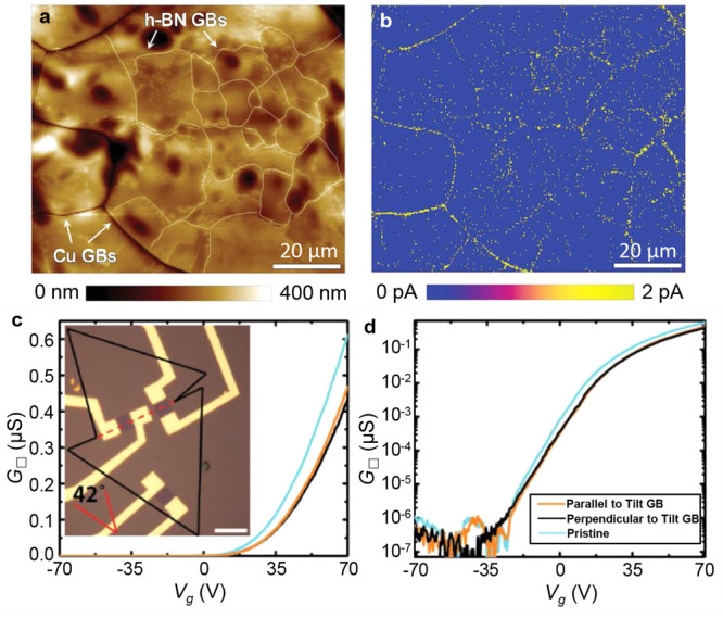
(a) Topographic and (b) current mapping of a polycrystalline hBN film (Reproduced from ref (18). Copyright 2021 Wiley). (c,d) Linear and logarithmic electrical transport transfer curves. (Reproduced from ref (20). Copyright 2013 Springer Nature).
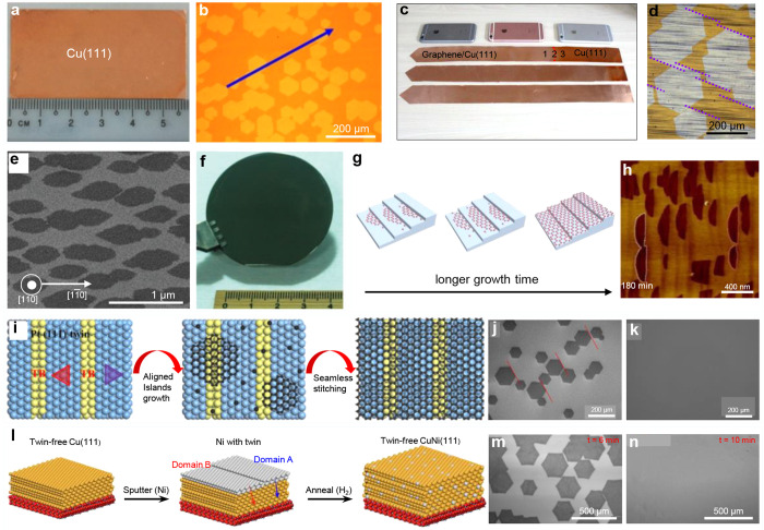
Graphene is the first discovered 2D material, and the growth of single-crystal graphene with meter scale has been achieved now.22−31 Highly aligned graphene islands can be obtained on Cu (111) due to the matched symmetry and small lattice mismatch.32 In 2015, Nguyen et al. successfully synthesized a 6 × 3 cm2 Cu (111) single crystal through repeated annealing and chemical mechanical polishing, enabling the growth of aligned graphene islands (Figure 2a,b).33 Furthermore, in 2017, Xu et al. developed a temperature-gradient-driving annealing method to produce meter-scale Cu (111) foils (Figure 2c) and achieved the largest single-crystal graphene within just 20 min using an ultrafast epitaxial growth technique (Figure 2d).22 Monolayer graphene single crystals have also been successfully grown on high-index Cu surfaces, including Cu (112), Cu (113), Cu (133), Cu (311), and Cu (436).34−36 Additionally, substrates like Ge (110), Ge (001), Pt (111), and CuNi (111) can also be utilized.37−40 For instance, Lee et al. and Li et al. synthesized wafer-scale single-crystal graphene on Ge (110) and 15° miscut Ge (001) substrates by precisely arranging all graphene islands, respectively (Figure 2e–h).37,38 Kang et al. reported the production of 6-in. single-crystal graphene on Pt (111) substrates through ambient-pressure chemical vapor deposition (CVD), as shown in Figure 2i–k.39 Deng et al., on the other hand, enhanced the catalytic activity of Cu by introducing a small amount of Ni and successfully prepared a 4-in. monolayer single-crystal graphene wafer on Cu90Ni10 (111) substrates in just 10 min (Figure 2l–n).40 Overall, significant advancements have been made in the production of large graphene single crystals.
Figure 2.
(a) Photograph of monocrystalline Cu (111). (b) Aligned graphene islands on Cu (111). (Reproduced from ref (33). Copyright 2015 Wiley). (c) Cu (111) foils covered with graphene. (d) Optical image of aligned graphene islands on Cu (111). (Reproduced from ref (22). Copyright 2017 Elsevier). (e) SEM image of graphene islands on Ge (110). (f) A photograph of the graphene wafer. (Reproduced from ref (37). Copyright 2014 American Association for the Advancement of Science). (g) Schematic diagrams of the growth process of single-crystal monolayer graphene. (h) AFM images of graphene islands on Ge (001). (Reproduced from ref (38). Copyright 2020 Elsevier). (i) Schematic of the growth of single-crystal graphene. (j,k) SEM images of graphene grown on Pt (111). (Reproduced from ref (39). Copyright 2021 Elsevier). (l) Schematic diagrams for the growth of single-crystal Cu90Ni10 (111). (m,n) SEM images of graphene with different coverage. (Reproduced from ref (40). Copyright 2019 Elsevier).
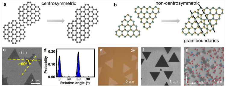
Unlike the growth of graphene, synthesizing single-crystal noncentrosymmetric 2D materials like hBN and TMDs is very challenging. In general, the commonly used substrates are centrosymmetric, resulting in only one orientation for centrosymmetric 2D materials (Figure 3a). When these islands merge together, they will be seamlessly stitched into single-crystal films. In contrast, the noncentrosymmetric 2D materials possess two energetically favorable antiparallel orientations. When these islands merge, grain boundaries will be formed (Figure 3b). For this reason, all of the earlier works could only produce antiparallel islands (Figure 3c–g).41−44
Figure 3.
(a,b) Schematic diagrams of centrosymmetric (a) and noncentrosymmetric (b) 2D materials when rotating for 180°. Grain boundaries will be formed for noncentrosymmetric 2D materials. (c) SEM images of hBN islands on Cu (111). (d) Statistical distributions of the edge angles of hBN islands. (Reproduced from ref (41). Copyright 2015 Springer Nature). (e) Optical image of 2H MoS2 monolayer flakes grown on mica. (Reproduced from ref (42). Copyright 2018 Springer Nature). (f) SEM images of MoS2 islands on GaN. (Reproduced from ref (43). Copyright 2016 American Chemical Society). (g) SEM images of WSe2 islands with antiparallel orientations. (Reproduced from ref (44). Copyright 2023 Springer Nature).
This review offers a comprehensive overview of the production of noncentrosymmetric 2D single crystals. First, we discussed the growth strategy of noncentrosymmetric 2D single crystals. Subsequently, our focus shifts toward the controlled growth methodologies applied to hBN, TMDs, and other representative noncentrosymmetric 2D materials. Lastly, we provide a concise summary of the challenges faced in this field and highlight intriguing avenues for future exploration.
2. Growth Strategy of Noncentrosymmetric 2D Single Crystals
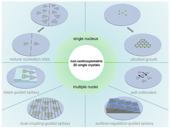
Under natural circumstances, 2D materials tend toward multinucleus growth with random orientations, resulting in the formation of polycrystalline films. This growth behavior is independent of the substrate materials. To obtain large 2D single crystals, stringent control is necessary. Generally, there are two strategies to produce single-crystal 2D materials: single-nucleus growth and multinuclei growth. For the growth from a single nucleus, the key is to reduce the nucleation density, allowing the growth of 2D materials from a single nucleus to a large-sized single crystal. For the growth from multiple nuclei, strict control of the nucleation density is not necessary, the key here is to accurately control the lattice orientations of the islands grown from different nuclei. If all islands possess identical lattice orientations, then these islands can be seamlessly stitched into large single-crystal films.
2.1. Growth from a Single Nucleus
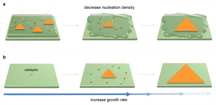
Effective control of nucleation during the initial growth stage is very important in determining the size and quality of single-crystal 2D materials. During the growth process, precursors tend to adsorb on defects, boundaries, particles, and other high-energy regions of the substrate, leading to nuclei formation with varying orientations.45−48 To reduce the nucleation density, one way is to resolidify the metal substrate.49,50 This melting process eliminates high-energy sites on the surface, resulting in an atomic flat surface and low nucleation density (Figure 4a). Another effective method is minimizing the amount of source as it makes nucleation more challenging and can effectively reduce the nucleation density. In addition to these methods, introducing additional elements such as oxygen has been found to significantly inhibit nucleation and facilitate large-sized single crystals.
Figure 4.
Schematic diagrams of single-crystal growth from a single nucleus by decreasing the nucleation density (a) and increasing the growth rate (b).
Increasing the growth rate is another effective aspect of single-nucleus growth. Since the nucleation is a random event, the shorter the growth time, the less additional random nucleation will occur. So, one can obtain large-sized single crystals in a very short time (Figure 4b).51
2.2. Growth from Multiple Nuclei
A promising strategy for achieving the growth of wafer-scale noncentrosymmetric 2D single crystals is seamlessly stitching together 2D islands with identical orientation. However, when noncentrosymmetric materials grow on high-symmetric surfaces, the emergence of antiparallel islands is inevitable.52−55 After a large number of attempts, there are currently four representative methods to achieve the orientation control of noncentrosymmetric 2D materials.53−61
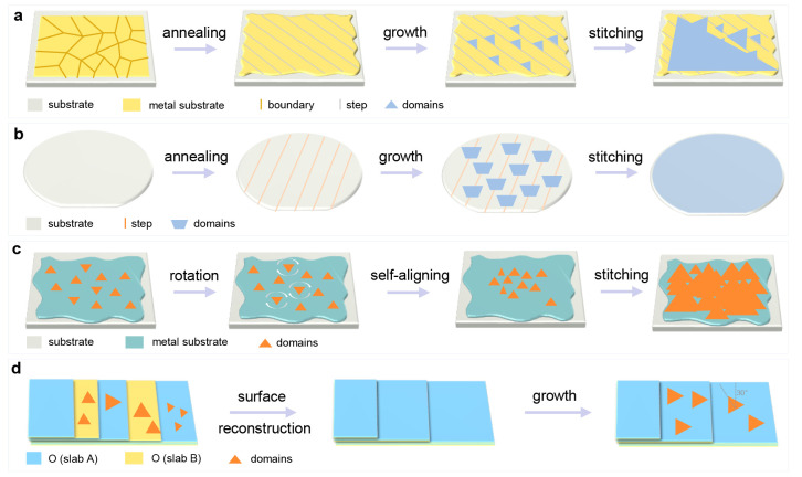
The first mechanism is the step-guided epitaxy. Extensive studies indicate that the steps on substrate are critical for adjusting orientations of as-grown islands. Parallel and flat atomic steps can be produced on the surface of single-crystal metal substrates after high-temperature annealing. These parallel steps have a significant impact on reducing the nucleation barriers and inhibiting upper step growth. These two aspects guarantee only one edge of the 2D materials aligned with the step edges, ensuring the single-crystal direction (Figure 5a).62,63
Figure 5.
Schematic diagrams of single-crystal growth from multiple nuclei. (a) Steps-guided epitaxy on metal substrates. (b) Dual-coupling-guided epitaxy on insulating substrate. (c) Self-collimation growth on molten substrates. (d) Surface reconstruction to guarantee single-crystal epitaxy.
The second mechanism is known as dual-coupling-guided epitaxy. Because the interaction between insulating substrates and 2D materials is much smaller than that between the metal substrate and the 2D materials. The presence of the steps cannot completely dominate the growth behaviors of these materials. In this case, a combination of van der Waals (vdW) interaction and steps interaction governs the growth mechanism, where the vdW interaction leads to two favored antiparallel orientations, while the steps interaction limits them to only one orientation. Consequently, these two interactions lead to the unidirectional alignment of the noncentrosymmetric 2D materials (Figure 5b).
Growth on the surface of molten metal is another technique for preparing single crystals. This method utilizes a synergistic self-collimation mechanism, which combines CVD growth kinetics with the rheological kinetics on the molten metal surface. As a result, triangular crystal islands floating on the surface can be rotated toward the same orientation. These islands then align themselves spontaneously due to mutual atomic attraction, leading to an aligned orientation and seamless stitching over a large area (Figure 5c).58
The final approach to tune the orientations of the noncentrosymmetric 2D materials is to reconstruct the surface of the substrates and this method does not need the existence of the steps. For instance, when 2D grains interact with the exposed oxygen–aluminum atomic surface, they can form an energy-optimized configuration known as a 2D grain-sapphire structure. By reconstructing sapphire substrates to consist solely of a single type of atomic plane, it is also possible to ensure single-crystal epitaxy of monolayer noncentrosymmetric 2D materials (Figure 5d).55
3. Growth of Single-Crystal hBN
hBN is a well-established noncentrosymmetric 2D materials, characterized by an alternating arrangement of boron and nitrogen atoms in its lattice. Its exceptional properties, including strong insulation, large nonlinear susceptibility, excellent chemical inertness, high thermal conductivity, and atomic flatness without dangling bonds make it highly suitable for potential applications in nanoelectronics, integrated photonics, quantum optics, and metal-corrosion protection.64−72 To realize such applications of hBN from lab to industry, the production of large-sized single-crystal hBN films is a prerequisite. Since the hBN films were synthesized through the CVD method on the nickel foils, significant efforts have been dedicated to produce hBN single crystals in the past decades.73−75
3.1. Growth of Single-Crystal hBN from a Single Nucleus
When hBN islands originating from different nuclei with random lattice orientations merge together, grain boundaries would be inevitably formed. Therefore, one straightforward approach to achieve hBN single crystals is to decrease the nucleation density and make the single nucleus grow up.
One widely employed approach is to pretreat the epitaxy substrate surface to suppress or passivate the nucleation sites, such as the steps and grain boundaries. Thus, utilizing electrochemically polished or secondary recrystallized metal substrates with smoother surfaces can effectively enhance the size of hBN islands.76,77 Additionally, doping other elements into the substrates has been proven to be an effective method. In 2015, Lu et al. introduced some Ni into Cu foils, resulting in a significant suppression of nucleation at both initial and subsequent growth stages (Figure 6a).78 As a result, the nucleation density was decreased to 60 mm–2, leading to an increase in the hBN island size to 7500 μm2 (Figure 6b). This alloying strategy also yielded favorable results on Si-doped Fe and Cu–Si substrates.79,80 Another effective approach for surface treatment is to preoxidize the epitaxy substrate before hBN growth. Taking Cu as an example, Chang et al. increased the binding energy of boron- and nitrogen-containing species by constructing a thin oxide layer on the Cu surface (Figure 6c).81 This resulted in a reduction of nucleation density from 106 to 103 mm–2, while improving the size of hBN islands to ∼20 μm (Figure 6d). Besides the formation of oxide layers, mild oxidation of the Cu foil can be achieved by introducing the trace O2 in Ar gas during the heating step. For example, Li et al. introduced copper oxide nanoparticles onto the surface.82 Typically, the nucleation density of hBN was highly limited down to 103 mm–2 by the number of nanoparticles, and the largest island size was observed to be more than 200 μm.
Figure 6.
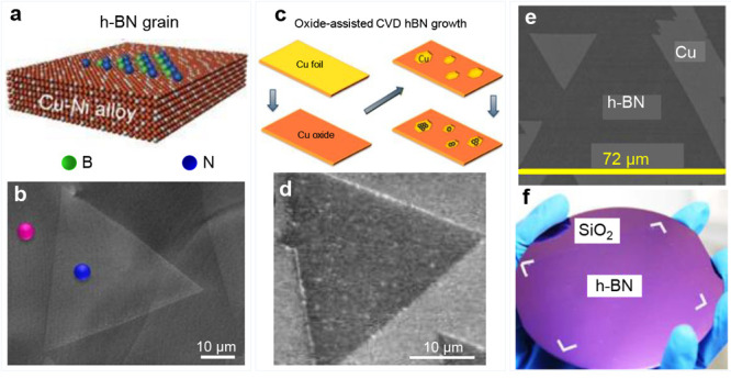
(a) Schematic diagram of hBN growth on Cu–Ni alloy. (b) SEM image of an hBN island. (Reproduced from ref (78). Copyright 2015 Springer Nature). (c) Schematic illustrations of the mechanism of hBN growth on preoxidized Cu. (d) SEM image of an hBN island. (Reproduced from ref (81). Copyright 2017 American Chemical Society). (e) SEM image of a large-domain hBN triangle. (f) Wafer-scale monolayer hBN film. (Reproduced from ref (41). Copyright 2015 Springer Nature).
Another approach to decrease the nucleation density is to limit the supply of boron- and nitrogen-containing precursors, typically achieved by folding the metal foil to create an enclosure and utilizing its inner surface as the growth substrate. In 2015, Song et al. reported their synthesis of a wafer-scale hBN monolayer, where a single island size is about ∼72 μm (Figure 6e).41 Moreover, they successfully transferred the monolayer film onto a target substrate like SiO2/Si wafer by the PMMA-assistant technique (Figure 6f). Furthermore, a larger hBN island with an edge length of ∼300 μm has been obtained by selecting an appropriate thickness of Cu foil.83 The utilization of the Cu enclosure could effectively reduce the nucleation density, while it would naturally decrease the precursor feeding rate, leading to a relatively lower production efficiency. To balance the growth rate and lateral size, Zhu et al. used a Cu–Ni gradient alloy enclosure to suppress the diffusion and enhance the decomposition to facilitate the growth of hBN and realized the lateral size of ∼60 μm.84 Furthermore, the effective modulation of nucleation density and growth kinetics can also be realized by introducing a suitable atmosphere such as hydrogen,85 ammonia,86 and water,87 or active species like fluorine.88
3.2. Growth of Single-Crystal hBN from Multiple Nuclei
Despite extensive exploration of nucleation control, the largest island size of single-crystal hBN remains limited to the submillimeter scale. As a result, while the grain boundaries can be dramatically reduced but inevitably exist when these islands coalesce within a wafer range. In order to achieve unidirectionally aligned growth of hBN islands, it is essential to tune the symmetry of the substrate.52 Wang et al. have predicted that tilting the Cu (101) facet along specific in-plane axes to form inclined surfaces can effectively tune the lattice symmetry and realize the single favored hBN orientation.89 This is consistent with the experimental result of aligned hBN islands grown on the Cu (102) and (103) surfaces.90 This approach is anticipated to be further developed with the availability of various high-index Cu foils.34
3.2.1. Step-Guided Epitaxy on Single-Crystal Substrates
The modulation of the hBN orientation is highly dependent on the strength of the vdW interaction between hBN and substrates, which might be relatively more susceptible to interference from external conditions. Single-crystal substrates with low-index surfaces, including (100), (110), and (111), are generally easier to obtain. Therefore, it is crucial to explore feasible methods for breaking the high lattice symmetry of these substrates and reliably locking the hBN orientation. Among these methods, constructing the atomic metal steps is a good choice.
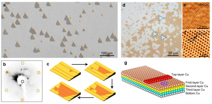
In 2019, Wang et al. achieved the successful alignment of hBN islands and subsequently achieved the growth of single-crystal films.56 Through the well-designed annealing process, they were able to obtain a 100 cm2 single-crystal Cu foil with vicinal (110) surface and atomic steps along ⟨211⟩ direction. Then unidirectional hBN islands with truncated triangle shapes were grown within the entire area (Figure 7a), with an alignment exceeding 99%. The same crystalline orientation was further confirmed by the low-energy electron diffraction (LEED) patterns collected at the multiple positions (Figure 7b). In situ SEM was used to monitor the growth behavior of single-crystal hBN, including the unidirectionally aligned nucleation alone the parallel steps, the anisotropic growth on the Cu surface, and seamless stitching into a large-sized single crystal (Figure 7c). This work demonstrated that the artificially constructed steps could effectively reduce the lattice symmetry of Cu (110) surface to C1, and the strong steps coupling between Cu and hBN enables the breaking of the energetic degeneracy of antiparallel hBN islands to finally achieve the production of single-crystal hBN monolayers.
Figure 7.
(a) SEM image of aligned hBN islands on Cu (110). (b) LEED pattern of hBN. (c) Schematic diagram of the growth process. (Reproduced from ref (56). Copyright 2019 Springer Nature). (d) Optical image of aligned hBN islands on Cu (111). (e,f) Atomic-scale STM images of hBN/Cu (111). (g) Theoretically calculated configurations. (Reproduced from ref (57). Copyright 2020 Springer Nature).
Moreover, the step-modulation method can also be employed to hBN grown on Cu (111). Chen et al. reported the successful preparation of single-crystal hBN monolayers on Cu (111) (Figure 7d).57 The atomic-resolution scanning tunneling microscopy (STM) characterizations show that the as-grown hBN on Cu (111) possessed the perfect crystal lattice (Figure 7e,f), exhibiting consistent lattice orientation over a wide range. Density functional theory (DFT) calculations were performed to reveal that this unidirectionally epitaxy was ensured by the lateral docking of hBN islands to the Cu (111) step edges (Figure 7g).
3.2.2. Self-Collimated Growth on Liquid Substrates
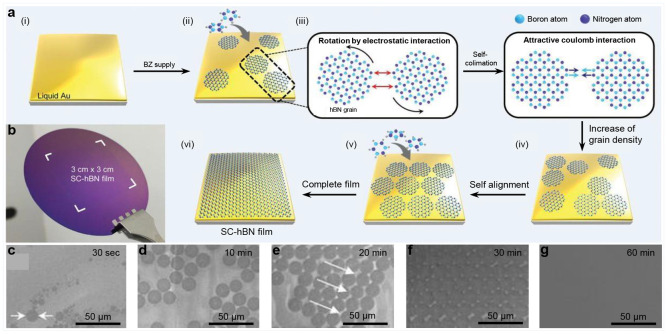
In addition to the introduction of metal steps, the symmetry of the substrate can also be broken on noncrystalline liquid metals. In 2015, Tan et al. successfully synthesized the self-aligned hBN arrays on a liquid Cu surface with uniform island sizes and consistent spatial orientations.91 Furthermore, Lee et al. proposed a self-collimation mechanism for growing wafer-scale monolayer hBN single crystals through the seamless stitching of hBN islands on a liquid Au surface (Figure 8a).58 The substrate was liquefied at an elevated temperature above the melting point of Au. The low solubility of B and N in Au ensured the high diffusion on such a flat surface to form isotropic circular hBN islands with a regular size of ∼14.5 μm. Afterward, the attractive Coulomb interaction between B and N atoms at the edge of different islands induced their rotation into a same orientation, and eventually stitched into single-crystal film (Figure 8b). The time-evolution SEM images captured at different growth stages comprehensively demonstrated the process of nucleation, lateral growth, coalescence, and full coverage (Figure 8c–g). The self-collimated synthesis technique was further developed by using a flowing liquid Cu surface.59 By synergistically controlling CVD growth kinetics and liquid Cu rheological kinetics, floating triangular hBN islands could efficiently self-align by rotation, and a centimeter-scale uniform quasi-single-crystal hBN film was finally obtained.
Figure 8.
(a) Schematic diagrams of the growth process of single-crystal hBN. (b) A photograph of a single-crystal hBN film. (c–g) SEM images of hBN at different growth time. (Reproduced from ref (58). Copyright 2018 American Association for the Advancement of Science).
3.3. Growth of Multilayer hBN
Multilayer hBN not only integrates the exceptional properties of its monolayer counterpart but also exhibits additional unique ones beyond monolayers, including stacking-dependent optical nonlinearity and interfacial ferroelectricity,92−96 the ability to prevent leakage and breakdown,97,98 as well as the infrared hyperbolic phonon polariton.99,100 In the past years, many kinds of attempts have been tried to synthesize the homogeneous large-scale hBN multilayers, including ion beam sputtering deposition (IBSD),101 molecular beam epitaxy (MBE),102−105 and metal–organic chemical vapor deposition (MOCVD),106 among which CVD is the most commonly used approach. However, a major challenge arises from the low solubility of B or/and N in epitaxial substrates, which dominates the self-limited growth mechanism of BN and hinders adlayer formation. To overcome this limitation, substrates with high solubility of B and N as well as long-range catalytic ability are extensively employed, leading to the development of various growth modes as discussed below.
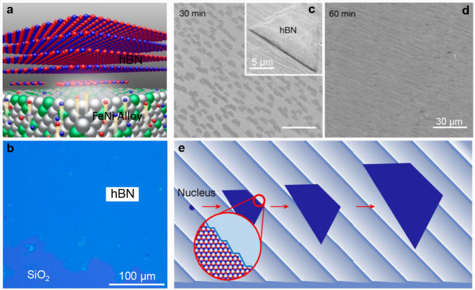
Highly catalytic active Pt was used to grow hBN multilayers, but its high cost hindered its further development.107 Polycrystalline Ni with the relatively high solubility of B atoms was first chosen as the substrate and realized the growth of multilayer hBN films with the thickness ranging from ∼5–50 nm.73 Further investigations revealed a linear dependence between the average thickness of hBN films and growth time, allowing for tunability from a few to several hundred layers.74 Besides Ni, Fe is another suitable substrate due to its high N solubility (∼8.0 atom % at 1000 °C) and its ability to readily react with B atoms, which can be dissolved into the Fe through a reaction-diffusion mechanism.108,109 Kim et al. synthesized the 3 × 3 cm2 multilayer hBN films with thickness up to 15 nm on Fe.110 The growth was mainly governed by the segregation of B and N atoms from iron bulk, rather than the surface-mediated Frank–van der Merwe model since the thickness and grain size were strongly dependent on the cooling rate. However, achieving a smooth surface for single crystal Fe poses a significant challenge due to its phase transition from a body-centered cubic (bcc) to face-centered cubic (fcc) structure at ∼912 °C. This naturally leads to the nonuniform precipitation and growth of hBN on the substrate. In 2018, Uchida et al. introduced the Ni atoms into Fe substrates to stabilize the fcc structure and adjust the solubility of B and N atoms, to finally realize the homogeneous segregation of hBN multilayers (Figure 9a,b).111 Fukamachi et al. successfully obtained a centimeter-scale multilayer hBN film with an average thickness of ∼6 nm and a low surface roughness of 0.19 nm by optimizing the growth parameters.112 In fact, during the epitaxial growth of single-crystal 2D materials, the orientation of the 2D lattice is closely associated with lattice matching and substrate surface steps, while the catalytic activity of the substrate primarily influences growth rate and nucleation through precursor decomposition and dissolution.113−116 It can be inferred that catalytic features of substrates play a secondary role in determining both the structure of the two-dimensional lattice and subsequent grain boundary formation. Therefore, all aforementioned hBN films are nonuniform and polycrystalline with massive grain boundaries, which hinder their high-end and industrial-level applications. Recently, Ma et al. realized the epitaxy of a 2 × 5 cm2 multilayer hBN single crystal with precisely controlled thickness on a stepped Ni (111) substrate.62 As shown in Figure 9c, the trilayer hBN nuclei were unidirectionally arranged on the Ni surface, and then synchronically grew up and seamlessly merged into a uniform single crystal (Figure 9d). Detailed AFM characterization and DFT calculation showed that the nucleation was guided by the Ni steps (Figure 9e).
Figure 9.
(a) Schematic of the growth process. (b) Optical image of hBN grown on Ni–Fe film. (Reproduced from ref (111). Copyright 2018 American Chemical Society). (c,d) SEM images of trilayer hBN islands at different growth time. (e) Illustration of hBN complementarity nucleation and growth process. (Reproduced from ref (62). Copyright 2022 Springer Nature).
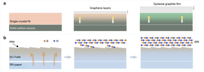
The production of thick hBN is also required in many scenarios. The solid substrates with a well-defined lattice structure may be a possible way. In 2022, Zhang. et al. reported the continuous epitaxial growth of centimeter-size single-crystal graphite films with thickness up to 100,000 layers on single-crystal Ni (520) foils by the isothermal dissolution–diffusion–precipitation (IDDP) process of carbon atoms (Figure 10a).117 Subsequently, this groundbreaking study was followed by the synthesis of uniform rhombohedral boron nitride (rBN) crystalline film using the same IDDP mechanism.118 To achieve this, single-crystal FeNi alloys which were chosen as the epitaxial substrate due to the high solubility of both boron and nitrogen. At the elevated temperature, the B and N atoms would continuously dissolve into the bottom surface of the FeNi alloy, diffuse through the whole metal, and finally precipitate on the top surface to layer-by-layer form the BN multilayers with the thickness up to 1 μm (Figure 10b).
Figure 10.
(a) Schematic diagrams for the continuous epitaxial growth of graphite. (Reproduced from ref (117). Copyright 2022 Springer Nature). (b) Schematic diagrams for the continuous epitaxial growth of rBN. (Reproduced from ref (118). Copyright 2023 Wiley).
4. Growth of Single-Crystal TMDs
2D TMDs have attracted great research interest due to the potential applications in the fields of electronics, optoelectronics, electrocatalysis, etc.119−121 To meet the requirements of high-end applications, it is necessary to prepare high-quality single-crystal TMDs with low-density defects.
4.1. Growth of Single-Crystal TMDs from a Single Nucleus
Currently, available TMDs usually exhibit uncontrolled layer number, small single-crystal size, and low growth rate.122 Achieving the growth of large monolayer TMDs single crystals is a fundamental challenge. It requires maximizing lateral growth rates while reducing the density as much as possible and has inspired considerable efforts.
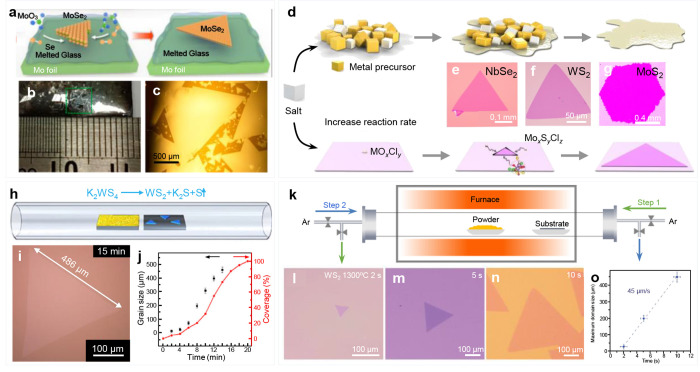
As commonly accepted, the nucleation tends to occur preferentially at the impurities and defects on the solid substrate. To promote the growth of large single crystals, complex procedures or surface treatments are necessary to inhibit the nucleation.48 In 2017, Chen et al. demonstrated the successful growth of millimeter-sized monolayer MoSe2 on molten glass using an ambient pressure CVD system (Figure 11a).50 The melting and subsequent regeneration of the glass result in a smooth surface. This “liquid-state” glass has an isotropic surface that significantly reduces the defects and enables low-density nucleation for large island growth. MoSe2 islands with large size (∼2.5 mm) and high carrier mobility (∼95 cm2 V–1·s–1) at room temperature can be synthesized quickly (Figure 11b,c). Additionally, it demonstrates the universality of this approach by successfully synthesizing millimeter-sized monolayer MoS2 as well.
Figure 11.
(a) Schematic diagrams for the production of MoSe2 monolayers. (b,c) Photograph and optical image of MoSe2 islands. (Reproduced from ref (50). Copyright 2017 American Chemical Society). (d) Schematics of the reactions. (e–g) Optical images of different TMDs monolayers. (Reproduced from ref (125). Copyright 2018 Springer Nature). (h) Schematic diagram for the set up. (i) Optical image of a WS2 island. (j) The evolution of domain size and coverage of the WS2 with growth time. (Reproduced from ref (126). Copyright 2020 Springer Nature). (k) Schematic illustration of a modified CVD system with reverse flow. (l–n) Optical images of WS2 synthesized at different times. (o) The maximum island size of WS2 as a function of growth time. (Reproduced from ref (132). Copyright 2020 Oxford University Press).
In addition, the production of many TMDs is challenging due to high melting points of the metal oxide precursors. To address this issue, molten salt-assisted methods have emerged to promote the growth of monolayer MoS2, WS2, and WSe2.123,124 In 2018, Zhou et al. reported the universality of molten salt-assisted CVD (Figure 11d) for synthesizing various TMDs.125 They successfully synthesized 47 compounds, including 32 binary compounds, 13 alloys, and two heterostructural compounds (Figure 11e–g). The presence of salt enables reactions with specific metal oxides to form metal chloride oxides that evaporate at lower temperatures, thus promoting the growth of 2D TMDs. During the growth process, a stable nucleus is formed through coarsening, and then adsorbed atoms and clusters of chalcogenide elements and metals attach to the edges of the growing 2D monolayer, exhibiting rapid growth.
Choosing a different type of precursor may offer a more direct and convenient route. Zhou et al. developed a controlled method for monolayer WS2 growth by CVD using K2WS4 as the precursor (Figure 11h).126 Unlike the use of WOx (x denotes the number of atoms) and S as precursors, this approach solely involves the thermal decomposition reaction of K2WS4, thereby enhancing the controllability of WS2 growth. The simple chemistry employed by this method improves controllability and allows for rapid growth rates of about 30 μm/min. This enables the growth of monolayer WS2 flakes up to ∼500 μm with low defect density, which exhibit superior electrical properties compared to the single crystals grown by prior methods (Figure 11i,j).
In the CVD process, reducing nucleation density is typically achieved by minimizing the feeding rate to minimize the probability of nucleation probability.127 But this significantly reduces the lateral growth rate (usually ∼1 μm/s or less).128 The growth of large monolayers often needs a long growth time, sometimes spanning hours or even longer to achieve millimeter-scale monolayers.129 Producing large single crystals with high growth rates is a key challenge in 2D crystal growth.130,131 In 2020, Zhang et al. used a counter-current reactor to achieve well-controlled nucleation and growth at high temperatures, thereby achieving ultrafast growth of large monolayer TMD single crystals (Figure 11k).132 Specifically, a reverse airflow is used during increasing the temperature to prevent accidental nucleation. This method effectively prevents nucleation and growth before the optimal growth temperature is reached. This, in turn, guarantees a plentiful supply of gas-phase reactants and adequate surface mobility, facilitating the fast growth. It is possible to obtain a maximum lateral growth rate of 45 μm/s (Figure 11i–o).
4.2. Growth of Single-Crystal TMDs from Multiple Nuclei
Currently, the size of monolayer TMDs single crystal prepared from one nucleus can reach millimeters, but it is still far away from the required wafer-scale single crystals. Then, the epitaxy growth from multiple nuclei was introduced. This method need a lattice-matched substrate for the epitaxy of TMD islands with uniform directions, followed by their coalescence into single crystals.133
4.2.1. Steps-Guided Epitaxial Growth
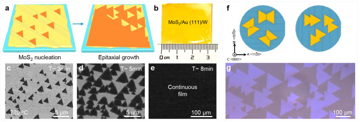
It has been demonstrated that single-crystal hBN can be obtained on vicinal Cu (110) substrates with parallel steps.56 Similarly, Yang et al. reported the epitaxy of monolayer MoS2 single crystals on vicinal Au (111) surface (Figure 12a,b).60 STM characterizations and first-principles calculations reveal that the nucleation of MoS2 is generally occurred on Au steps, leading to unidirectional MoS2 islands along the step edges and finally stitched to a continuous film (Figure 12c–e). In addition, it was found that the formation of 60°-oriented islands can be inhibited by precisely regulating the S/Mo ratio. Overall, this work presents a direct approach for synthesizing centimeter-scale TMD single crystals on metal substrates.
Figure 12.
(a) Schematic diagrams for the growth of single-crystal MoS2 on Au (111). (b) A photograph of the MoS2/Au (111). (c–e) SEM images of aligned MoS2 islands with different growth time. (Reproduced from ref (60). Copyright 2020 American Chemical Society). (f) Schematic diagrams of MoS2 islands on C/M and C/A sapphire (0001). (g) Optical image of MoS2 islands. (Reproduced from ref (54). Copyright 2021 Springer Nature).
Considering the practical applications of TMDs films, achieving direct synthesis on insulating substrates is the ultimate goal. Sapphire has been extensively employed as an epitaxial substrate.134 Li et al. designed a cross-cut direction toward the sapphire’s A-axis to prepare a 2-in. monolayer MoS2 single crystal (Figure 12f,g).54
4.2.2. Dual-Coupling-Guided Epitaxial Growth
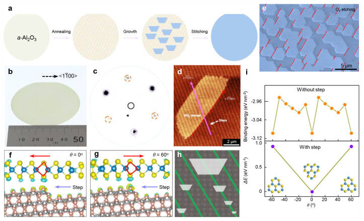
Step-guided growth of noncentrosymmetric 2D materials needs strong couplings between the 2D materials and step edges to guarantee the unidirectional alignment. However, for the insulating sapphire substrates, such strong edge-step coupling may not be feasible. Therefore, the epitaxy mechanism of 2D TMDs on insulating substrates may be significantly different from that on metal substrates. Wang et al. have proposed some guidelines for selecting a suitable insulating substrate.61 Vicinal a-plane sapphire (a-Al2O3) was first annealed at high temperatures in an O2 atmosphere to stabilize the parallel atomic steps. These atomic step edges were intentionally engineered to break the C2 symmetry and direct the aligned growth of WS2 islands (Figure 13a). Then, a 2-in.-sized single-crystal WS2 monolayer was successfully synthesized (Figure 13b). LEED, second-harmonic generation (SHG) and O2 etching evaluations confirmed that the film was formed by unidirectionally aligned WS2 islands (Figure 13c and e). High-resolution AFM images of WS2 islands further confirmed existence of parallel steps, along with the lattice orientation of WS2 and sapphire (Figure 13d). Based on theoretical analysis and DFT calculations, the authors discovered that the epitaxy of WS2 on a-Al2O3 surface is governed by a dual-coupling-guided mechanism. (Figure 13f–i).
Figure 13.
(a) The growth process of single-crystal WS2 films on a-Al2O3. (b) A photograph of WS2/a-Al2O3. (c) Representative LEED pattern of the WS2 film. (d) AFM image of a WS2 island. (e) False-color SEM image of WS2 films after O2 etching. (f,g) Optimized structures of antiparallel WS2 on a-Al2O3. (h) Schematic of WS2 islands grown on a-Al2O3 during the early stage of growth. (i) Theoretical analysis and DFT calculation of WS2 epitaxial growth with and without steps. (Reproduced from ref (61). Copyright 2022 Springer Nature).
4.2.3. Surface-Reconstruction-Guided Epitaxial Growth
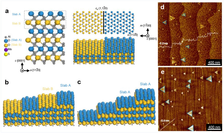
The prevailing view is that the alignment of 2D TMDs grain is primarily driven by step-edge-guided epitaxy. However, Fu et al. have indicated that the interaction of 2D TMDs grains and exposed O–Al atomic planes can also play a significant role in achieving the unidirectional alignment.55 This interaction leads to a minimized energy structure of 2D TMDs grains on c-Al2O3 regardless of the cutoff tilt angle (Figure 14a–c). When the type of steps is alternating slabs of A and B, the orientation of the MoS2 nucleus growing on two neighboring steps is antiparallel (Figure 14d). In contrast, unidirectional growth of MoS2 can be achieved when a single type of step is formed over the entire surface of the sapphire substrate (Figure 14e). The cross-sectional transmission electron microscopy (TEM) image confirms that the step height is ∼0.4 nm, and the monolayer MoS2 grows seamlessly along the a/a terrace. Therefore, the preparation of the appropriate atomic surface structure is also important to the growth of single crystals.
Figure 14.
(a–c) Schematic diagrams of sapphire surface with 3-fold atomic arrangement. (d,e) AFM images of antiparallel and unidirectional aligned MoS2 islands. (Reproduced from ref (55). Copyright 2023 Springer Nature).
4.2.4. Simultaneous Formation of Grain Nuclei and Substrate Steps
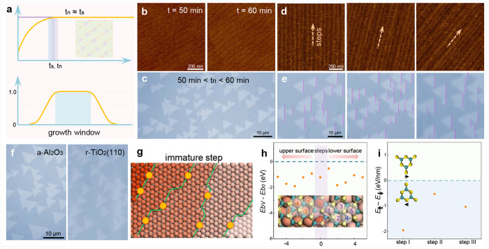
Although unidirectionally aligned TMDs have been achieved by many groups, the antiparallel islands during epitaxial growth were reported by more works, even on the same substrate.135−153 Currently, experimental window for epitaxial growth of noncentrosymmetric 2D materials is very narrow, and the key mechanism for ensuring such epitaxy remains unclear. In 2023, Zheng et al. highlighted that the time of TMDs nucleation (tn) and the substrate steps formation (ts) is critical for single-crystal growth.53 When tn ≈ ts, immature step edges become active sites for 2D grain nucleation, ensuring unidirectional alignment in a broad growth window (Figure 15a). AFM images reveal the parallel steps after annealing for ∼200 min (Figure 15b). Unidirectionally aligned MoS2 grains are easily achieved on c-Al2O3 substrate when tn ≈ ts (Figure 15c). Notably, among the nine tested step orientations, all grown MoS2 grains aligned along the same direction of the c-Al2O3 surface (Figure 15d,e). This technique is also applicable to other substrates (Figure 15f). The epitaxy can extend to other TMDs like WS2, NbS2, MoSe2, WSe2, and NbSe2. DFT results provide insights into the mechanism of the universal epitaxy. During annealing, most oxygen vacancies disappeared, except for those near steps (Figure 15g). The negative value of the binding energy of a MoS2 grain on a step without/with O vacancy (EbV – Eb0) suggests stronger interaction of MoS2 grains with defective steps (Figure 15h). Then antiparallel MoS2 grains can be effectively distinguished (Figure 15i).
Figure 15.
(a) Schematic illustration of the growth process of MoS2. (b) AFM images of vicinal c-Al2O3 surfaces annealed at different times. (c) Optical images of MoS2 grains on c-Al2O3 at 50–60 min. (d) AFM images of the c-Al2O3 surface. (e) Optical images of MoS2 grains on c-Al2O3 substrates. (f) Optical images of MoS2 grains on a-Al2O3 and r-TiO2 (110) substrates. (g) Schematic diagrams of the c-Al2O3 surface during annealing at high temperature. (h) The binding energy difference of a MoS2 grain on a step without/with O vacancy. (i) Energy difference between two antiparallel MoS2 grains across different steps. (Reproduced from ref (53). Copyright 2023 Springer Nature).
4.3. Growth of Bilayer and Multilayer TMDs
To date, a wide range of high-quality monolayer TMDs chips have been successfully fabricated, ranging from individual transistors to integrated circuits. Compared to the monolayer TMDs, the multilayer ones exhibit a narrow band gap with enhanced carrier mobility and photon absorption ability.154,155 However, achieving uniform high-quality multilayer TMDs single crystals remains an ongoing challenge. The main challenges for the growth of bilayer/multilayer TMDs single crystals are as follows: (i) Bilayer/multilayer TMDs have a higher nucleation barrier compared to monolayers, making it more preferable to grow monolayers on most substrates. (ii) The strong vdW interaction between the substrate and epitaxial TMDs makes it challenging to obtain uniform bilayer/multilayer films, with upper layer growth being more difficult than the lower layer.
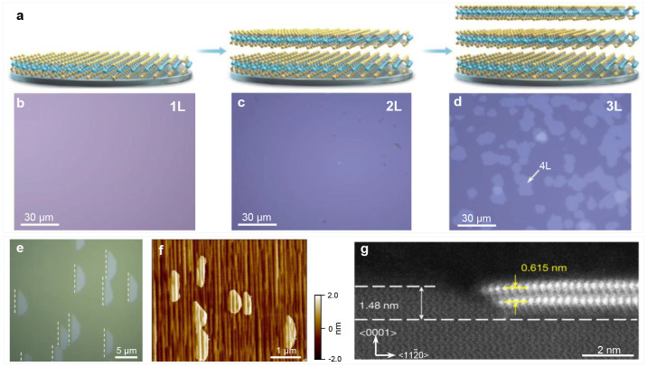
To produce uniform TMDs bilayers, two approaches can be chosen, namely layer-by-layer growth and edge-guided bilayer nucleation and growth. In 2022, Wang et al. grew 4-in. high-quality multilayer MoS2 wafers with a controlled number of layers (Figure 16a).156 First, they used oxygen-assisted CVD to break the self-limiting growth of MoS2 monolayers and reduce the reaction energy barriers during the growth process. Second, they elevated the temperature of the MoO3 and substrate to increase the nucleation density and edge growth rate of the second layer. Finally, uniform NL-MoS2 (N = 1, 2, 3) growth was successfully achieved in a layer-by-layer manner with epitaxy process repeated, where N is the layer number (Figure 16b–d). During the same period, Liu et al. reported the uniform bilayer MoS2 on c-Al2O3 using the bilayer nucleation strategy.157 The height of the steps is designed to realize the edge nucleation and MoS2 island coalescence into continuous centimeter-level films (Figure 16e–g). They achieved a six-step terrace matching the height of bilayer MoS2 by annealing the c-Al2O3 at high temperature. Meanwhile, they increased the concentration of precursors to ensure the formation and growth of bilayer nuclei.
Figure 16.
(a) Schematic diagrams of epitaxy growth. (b–d) Optical images of MoS2 with different layer. (Reproduced from ref (156). Copyright 2022 Oxford University Press). (e) Optical image and (f) AFM image of bilayer MoS2 islands. (g) Cross-sectional STEM image of bilayer MoS2. (Reproduced from ref (157). Copyright 2022 Springer Nature).
4.4. Growth of Stacking-Controlled TMDs
When putting 2D monolayers together, the weak vdW coupling allows for various interlayer stacking configurations. Taking TMDs as an example, the monolayers will rotate 60° to each other to form the centrosymmetric hexagonal stacking structure (2H) or parallelly stack with the same direction to obtain the noncentrosymmetric rhombohedral stacking sequence (3R).158
Previously, Zhang et al. achieved a series of large-sized TMDs bilayers with different stacking through the reverse-flow chemical vapor epitaxy.159 They first grew the monolayer TMDs on the substrate at a lower temperature (700 °C), then increased the temperature to make the vertical epitaxial growth of the second monolayer more easily than the lateral epitaxy. At the preferred growth temperature, 3R- and 2H-TMDs bilayers were successfully obtained. While the universal growth of the large-scale single-crystal pure-phase 3R-TMDs multilayer films remains a great challenge but urgent need for development due to their higher mobility,158 stronger optical nonlinearity,160,161 interlayer ferroelectricity, etc.162,163
4.5. Growth of Twist-Controlled TMDs
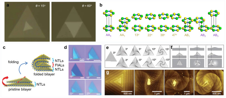
Besides the commensurate stacking configuration with the interlayer angles of both 0° and 60°, the twistedly stacked 2D multilayers have attracted widespread interest in the past few years. In 2014, Liu et al. grew the bilayer MoS2 islands with various twist angles by a regular CVD method (Figure 17a) and found that the incommensurate stacking order would enlarge the separations between two MoS2 monolayers, resulting in the reduction of the interlayer coupling (Figure 17b).164 The centimeter-scale bilayer MoS2 homostructures with the precise control of interlayer twist angle (accuracy of ∼2°) were realized by growing monolayer MoS2 combined with a water-assisted clean transfer method.165 Recently, a method to grow large twist bilayer graphene (TBG) with controlled angles was explored.166 In detail, the twist angle of TBG was docked by the two prerotated Cu (111) substrates to form a Cu/TBG/Cu sandwich structure, and then an equipotential surface etching process was applied to isolate the TBG film. Such growth technique may be extended to achieve the large-sized growth of twist bilayer TMDs with the more precisely controlled twist angle.
Figure 17.
(a) Optical images of twisted bilayers MoS2. (b) Schematics of MoS2 bilayers different twisted angles. (Reproduced from ref (164). Copyright 2014 Springer Nature). (c) The illustration of the folding process. (d) Optical microscopy images of folded bilayer MoS2 with different twist angles. (Reproduced from ref (169). Copyright 2022 Wiley). (e) Simulated superstructures of triangular dislocation spiral. (f) Aligned spirals, fastened supertwisted spiral and unfastened supertwisted spiral. (g) AFM images of aligned WS2 spirals and representative WS2 supertwisted spirals with various twist angles. (Reproduced from ref (172). Copyright 2020 American Association for the Advancement of Science).
The fabrication of twist-stacked 2D multilayers has also made some progress. Traditionally, the twisted multilayer superlattices are obtained by artificially stacking the selected flakes.167,168 Zhang et al. realized the twisted MoS2 multilayers by the paraffin-assisted folding of nontwisted ones (Figure 17c).169 The twist angle could be well controlled ranging from around 3° to 27° (Figure 17d). For creating the high-order twisted superlattice with multiple twisted interfaces, also named spiral or screw structure, the CVD growth technique is a widely used route.170,171Figure 17e showed the shapes of a range of twisted superstructures.172 Through the geometric and mathematical analysis, the growth behavior of twisted multilayer was found to be extremely dependent on the morphology of the substrate surface, e.g., an unfastened supertwisted spiral would be grown on a protruded substrate (Figure 17f). Finally, such supertwisted spirals of WS2 and WSe2 were successfully grown on the non-Euclidean surface of SiO2/Si substrates (Figure 17g).
4.6. Growth of TMD Heterostructures
All above-mentioned TMDs are of the homostructures, and combining them together as heterostructures in either lateral or vertical directions will bring novel properties and potential applications. Various approaches have been employed to synthesize these fashionable and functional heterostructures.
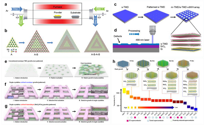
The in-plane heterostructures were generally obtained by the epitaxy of the subsequent components at the edge of the existing 2D materials. In 2017, Zhang et al. reported a reverse-flow synthetic strategy (Figure 18a),173 where the substrate-to-source or source-to-substrate flow was alternatively applied to prevent undesired thermal degradation of the as-grown 2D crystals (step 1) or transport the growth sources for the epitaxy of the target ones (step 2), to obtain the various lateral heterostructures and even superlattices (Figure 18b). Subsequently, a one-pot growth method was proposed to synthesize the multiheterojunctions by the precise modulation of gas with water vapor, which would help the oxidation, volatilization, and nucleation of the transition-metal sources, and sequential edge epitaxy of the TMDs monolayers.174 Furthermore, the arrayed heterostructure monolayer films were realized by using the specific laser patterning and thermal etching process on the existing monolayer and following the epitaxial growth of another 2D crystal.175 These works with sharp interfaces have built up a rationally designed platform for the further development of integrated 2D lateral heterostructures based on the mature growth technique of large-scale single-crystal monolayers.
Figure 18.
(a) Schematic diagrams of the CVD system. (b) 2D monolayer seed, and heterostructures. (Reproduced from ref (173). Copyright 2017 American Association for the Advancement of Science). (c) Schematic diagrams of the growth process of TMDs. (d) Schematic diagram of the laser-patterning process. (Reproduced from ref (176). Copyright 2020 Springer Nature). (e) Schematic of the general process by which TMDs are grown. (f) Schematic of the selective single-island synthesis strategy. (g) Single-island MoS2/WSe2 heterostructures by confined growth of a second MoS2 layer. (Reproduced from ref (177). Copyright 2023 Springer Nature). (h) Stacking growth of vdW superconductor heterostructures guided by the high-to-low temperature strategy. (Reproduced from ref (178). Copyright 2023 Springer Nature).
The vertical heterostructures can be fabricated by artificially stacking the vdW 2D materials via a polymer-assisted dry-transfer method. The direct heteroepitaxy, possessing better contact and a cleaner interface without the resident dopants, is expected to be scalable for practical applications. As shown in Figure 18c, the nucleation and vertical epitaxy of various metallic TMDs enabled to be precisely controlled by the selectively patterned nucleation sites on the existing monolayer or bilayer semiconducting TMDs through the focused laser irradiation (Figure 18d).176 In the meanwhile, Kim et al. proposed a geometric-confinement growth technique to obtain large-area 2D monolayer arrays and their heterostructures on various substrates.177 The traditional CVD growth of monolayer TMDs films would generally involve the random nucleation and the formation of grain boundaries (Figure 18e). In contrast, they selectively constructed the growth areas via patterning SiO2 masks to confine the monolayer or heterostructures only growing into these areas rapidly from the single nucleus to eventually form the single islands (Figure 18f,g). Recently, wafer-scale multiple-layered heterostructures, ranging from double- to five-block layers, have been realized via a high-to-low temperature growth strategy in the two-step vapor-deposition system.178 This success mainly relied on the relatively lower growth temperature of the subsequent component than that of the existing one (Figure 18h). The well designed interfaces with very little contamination between the adjacent layers was also demonstrated by the detailed characterizations. Based on these works, the rationally designed synthesis of single-crystal multilayer heterostructures with tunable components and atomically sharp interfaces on a large scale is highly desired.
5. Growth of Other Noncentrosymmetric 2D Materials
5.1. Growth of 2D Elemental Materials
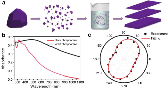
Besides graphene, other 2D elemental materials such as phosphene (black phosphorus, BP), silicene, germanene, and tellurene have also attracted substantial attention owing to their notable properties, including high carrier mobility, strong in-plane anisotropy, and adjustable bandgap.179−183 Most of these 2D elemental materials are centrosymmetric. However, in 2020, Zhang et al. successfully synthesized noncentrosymmetric violet phosphorus single crystals, providing the first reliable lattice structure.184 Subsequently, Ma et al. achieved the exfoliation of violet phosphene through sonication in ethanol (Figure 19a).185 The crystal structure of violet phosphine exhibits lower symmetry due to its vertically stacked interlocking cross-chain arrangement. The ultraviolet–visible–near–infrared (UV–vis–NIR) absorption spectra demonstrate the enhanced light absorption of violet phosphene in the visible and infrared regions compared to BP (Figure 19b). Polarization measurements of violet phosphine reveal varying SHG responses dependent on the polarization angles, consistent with the 2-fold rotational symmetry of its crystal structure (Figure 19c).
Figure 19.
(a) The preparation processes, (b) UV–vis–NIR absorption spectrum of violet phosphorene. (c) The angle-dependent SHG polarization pattern. (Reproduced from ref (185). Copyright 2023 Wiley).
5.2. Growth of 2D Group III Monochalcogenides
Among the group III monochalcogenides, In2Se3 stands out as a captivating 2D ferroelectric material because of its intrinsic properties of direct band gap (1.36 eV), multiphase, and in-plane and out-of-plane polarizations. These distinctive properties make it highly suitable for the applications such as electromechanical transducers, phase-change memories, optoelectronics, and photovoltaics.186−191
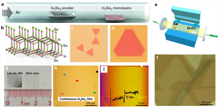
In 2015, Zhou et al. employed physical vapor deposition to produce a high-quality α-In2Se3 monolayer (Figure 20a).192 The α-In2Se3 monolayer consists of a quintuple layer with vertically aligned “Se–In–Se–In–Se” with “Se–In–Se” stacking on one side and “Se–In” stacking on the other (Figure 20b). Different growth times can obtain triangular In2Se3 monolayers and multilayers (Figure 20c,d). Then, Feng et al. successfully achieved the epitaxial growth of large-scale 2D In2Se3 nanosheets with a lateral size of ∼100 μm on a mica substrate (Figure 20e,f).193 More recently, He et al. demonstrated the growth of larger-area In2Se3 films via selenylation of In2O3 using the CVD method.194 Notably, the size of continuous In2Se3 films grown on a mica substrate can reach 1 × 1 cm2 (Figure 20g–i).
Figure 20.
(a,b) PVD growth process and crystal structure of monolayer In2Se3. (Reproduced from ref (192). Copyright 2015 American Chemical Society). (c,d) Optical images of In2Se3. (e,f) Schematic diagram of the CVD setup and optical image of 2D In2Se3. (Reproduced from ref (193). Copyright 2016 American Chemical Society). (g) Photograph of the bare mica substrate and the In2Se3 film. (h) Optical image of the In2Se3 film. (i) AFM image of the In2Se3 film. (Reproduced from ref (194). Copyright 2023 American Chemical Society).
5.3. Growth of 2D Group IV Monochalcogenides
Group IV monochalcogenides (MXs, where M = Sn or Ge and X = S or Se) have attracted substantial attention due to their unique orthorhombic structure, eco-friendly nature, resource abundance, and cost-effectiveness.195−199 Especially, their vdW structure can yield significant in-plane piezoelectric properties and pronounced anisotropy.200 These properties make them promising candidates for broad-scale utilization in photovoltaic and thermoelectric applications.201−203
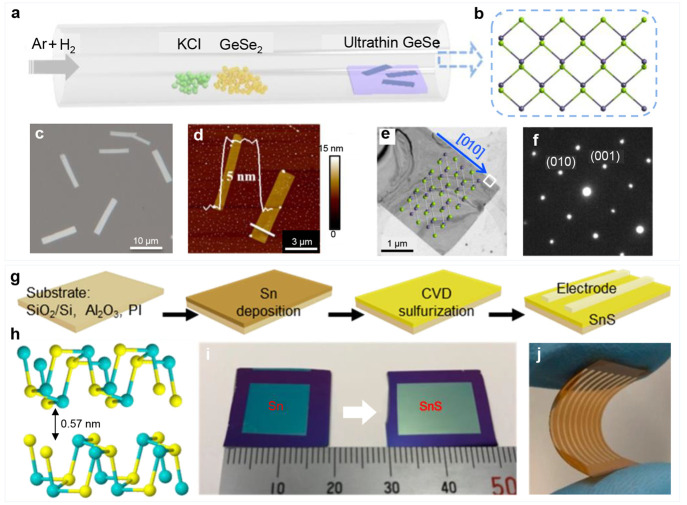
Synthesizing ultrathin GeSe is very challenging due to the strong interlayer forces and complex phases.204 Taking inspiration from the successful growth of 2D TMDs using the molten salt-assisted CVD method, Hu et al. employed a similar approach to produce ultrathin 2D α-GeSe flakes (Figure 21a,b).205 Ultrathin 2D α-GeSe flakes grown on mica substrates exhibit dimensions of 3 μm in width and 15 μm in length with a minimal thickness of 5 nm (Figure 21c–f). To ensure compatibility in the output and fabrication of piezoelectric devices based on MXs with inherent piezoelectric properties, Yoo et al. conducted the synthesis of centimeter-scale 2D SnS layers on various substrates via vulcanization of predeposited Sn film (Figure 21g,h).206 The scalability of this growth method is demonstrated by successful production of 2D SnS films exceeding 1.5 cm2 (Figure 21i). Notably, the growth temperature is as low as 200 °C, which is tolerable for a wide range of polymer substrates. This enables the direct growth of SnS on polyamides (PIs, 50 μm) substrates with integrated gold electrodes while maintaining excellent mechanical properties (Figure 21j).
Figure 21.
(a) Schematic diagram of the setup. (b) Structure of layered GeSe. (c,d) Optical and AFM images of synthesized GeSe. (e,f) Low-magnification TEM image and electron diffraction pattern of a GeSe flake. (Reproduced from ref (205). Copyright 2019 American Chemical Society). (g) Procedures for the growth of SnS. (h) Structure of orthorhombic 2D SnS layers. (i) Patternable and scalable growth of 2D SnS layers. (j) Flexible 2D SnS layers grown on PI substrates. (Reproduced from ref (206). Copyright 2023 American Chemical Society).
5.4. Growth of 2D Group III–IV Binary Compounds
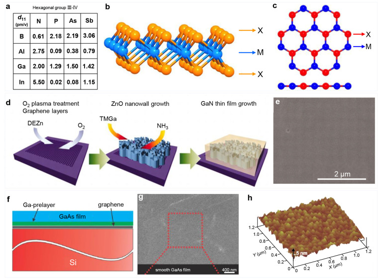
Some 2D group III–IV binary compounds break the inversion symmetry of the crystal structure, thereby exhibiting piezoelectricity and demonstrating an in-plane piezoelectric coefficient (Figure 22a–c).207 In addition, GaN and GaAs offer numerous advantages for optoelectronic device applications due to their high carrier mobility and long-term stability.208−211 Chung et al. successfully grew GaN films on graphene layers utilizing densely aligned ZnO nanowalls as an intermediary substrate (Figure 22d).212 The initial step involved plasma oxygen treatment of the graphene, creating distinct stepped edges. Subsequently, high-density ZnO nanowalls were grown on the graphene substrate. Given the minimal lattice mismatches between ZnO nanowalls and GaN, it became possible to achieve lateral epitaxy for GaN films on these nanowalls (Figure 22e). In 2014, Alaskar et al. demonstrated the first growth of ultrasmooth GaAs films on graphene/silicon substrates using quasi-vdW epitaxy.213 The employment of Ga-prelayers could produce a smooth surface (Figure 22f). Besides the impact of the Ga coating, the lower growth rate is also helpful for the smooth GaAs surface (Figure 22g,h).
Figure 22.
(a) Periodic trends for d11 in group III–V semiconductors. (b,c) 2H and planar hexagonal structures of group III–V semiconductors. (Reproduced from ref (207). Copyright 2015 American Chemical Society). (d) Schematic diagrams of epitaxial growth of GaN thin films. (e) GaN thin film grown on ZnO nanowalls. (Reproduced from ref (212). Copyright 2010 American Association for the Advancement of Science). (f) Schematic diagram of cross-section view of the GaAs films/Ga-prelayer/graphene/Si. (g) SEM plan-view image and (h) AFM image of ultrasmooth GaAs films. (Reproduced from ref (213). Copyright 2014 Wiley).
5.5. Growth of 2D Ternary Compounds
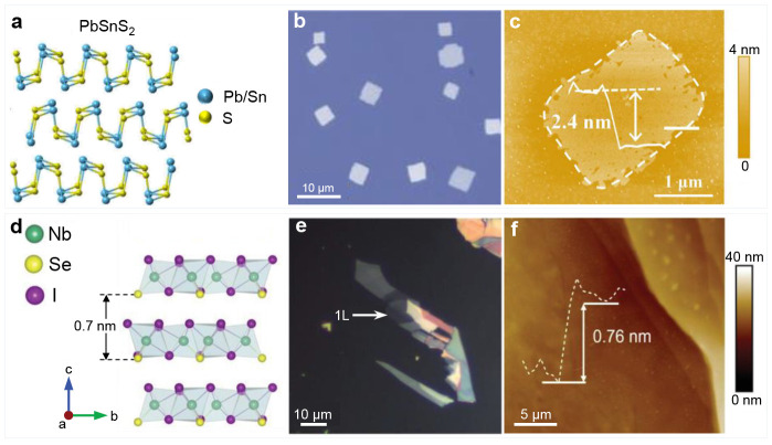
Beyond 2D binary materials, the presence of variable stoichiometry in 2D ternary materials provides additional degrees of freedom.214−217 Shu et al. have introduced a novel CVD method for synthesizing ultrathin PbSnS2 flakes using salt (KCl) and molecular sieves (Na12[(AlO2)12(SiO2)12]-xH2O, where x denotes the water crystals number).218 This method effectively lowers the metal precursor’s melting point by adsorbing and trapping evaporated molecules, ensuring a uniform distribution of the source (Figure 23a–c). More recently, Wang et al. reported the synthesis of Nb3SeI7, a new ternary layered material via chemical vapor transport (CVT).219 Nb3SeI7 possesses a noncentrosymmetric lattice structure and exhibits pronounced SHG, in-plane anisotropic electrical properties, and optical absorption capabilities (Figure 23d–f).
Figure 23.
(a) The atomic structure of PbSnS2. (b) Optical image of PbSnS2 nanoplates. (c) AFM image of a PbSnS2 flake. (Reproduced from ref (218). Copyright 2020 Elsevier). (d) Crystal structure of Nb3SeI7. (e) Bright-field optical images of Nb3SeI7 with varied thicknesses. (f) AFM image of monolayer Nb3SeI7. (Reproduced from ref (219). Copyright 2023 Wiley).
Overall, most of the current works on the production of noncentrosymmetric 2D single crystals are focused on the hBN and TMDs. For the noncentrosymmetric 2D materials mentioned in this section, including 2D elemental materials, 2D group III monochalcogenides, 2D group IV monochalcogenides, 2D group III–IV binary compounds, and 2D ternary compounds, there remains ample scope for advancements in the synthesis of their single crystals. Presently employed methods only yield a limited number of individual islands or polycrystalline films. The control over nucleation density and lattice orientation in these materials is still at an early stage with scarce reports available. Therefore, further exploration and research are imperative for future investigations.
6. Conclusion and Perspective
In conclusion, the precise preparation techniques of single nucleus control and multiple nuclei collaboration for wafer-scale single-crystal noncentrosymmetric 2D materials, especially monolayer films, have significantly advanced for their high-end applications. This review provides a comprehensive summary of the recent advancements achieved in this field. However, to successfully integrate 2D materials into real production processes, several requirements must be met. These include achieving extreme uniformity and repeatability of crystal quality,220 ensuring all-component growth or ultraclean transfer on Si-based wafers,221−223 implementing low-temperature single-crystal preparation,224,225 as well as attaining controllable dopant distributions and doping levels.226,227
In the meantime, multilayer noncentrosymmetric 2D materials with higher device performance (including mobility, on–off ratio, and electrostatic control),228,229 lower integration threshold,230 and novel physical properties (strong-correlated states, sliding ferroelectricity, moiré excitons, etc.),231−234 have been highly desired. However, both R- and H-stacked 2D materials exhibit similar formation energies, resulting in uncontrolled stacking structures and unavoidable grain boundaries. The epitaxial growth of 2D heterostructures also encounters this issue, as different configurations possess comparable energies. Similar to the growth of monolayer noncentrosymmetric 2D single crystals, this energy degeneracy may also be addressed by introducing steps, but certainly requires more precise control.
In terms of twist angle, the continuous twisting of superlattices has been limited to the single-island scale due to thermodynamic instability. This thermodynamic instability may be solved by introducing additional degrees of freedom. For instance, a seed crystal with adjustable angle can be placed on the first layer of material to achieve epitaxial growth of angle-controlled 2D materials.
In conclusion, significant advancements have been achieved in the production of monolayer single-layer 2D materials thus far, leading to the development of integrated devices that exhibit exceptional performance. The number of layers, twist angle, and stacking configurations can offer novel opportunities for controlling the physical properties of 2D materials, and the consequent revolutionary applications. Therefore, the production of 2D single crystals will continue to be a crucial research focus in the forthcoming decade.
Acknowledgments
This work was supported by Guangdong Major Project of Basic and Applied Basic Research (2021B030103000), the National Natural Science Foundation of China (12322406, 52102043, 52025023, 51991342, 52021006 and 61905215), the Key R&D Program of Guangdong Province (2020B010189001, 2019B010931001, 2018B010109009 and 2018B030327001), the Pearl River Talent Recruitment Program of Guangdong Province (2019ZT08C321), the Key Project of Science and Technology of Guangzhou (202201010383), the Natural Science Foundation of Guangdong Provinces (2023A1515012743), the Strategic Priority Research Program of Chinese Academy of Sciences (XDB3300000), and the New Cornerstone Science Foundation through the XPLORER PRIZE.
Author Contributions
# G.C., J.Q., Z.L., and F.Z. contributed equally to this work
The authors declare no competing financial interest.
References
- Novoselov K. S.; Geim A. K.; Morozov S. V.; Jiang D.-e.; Zhang Y.; Dubonos S. V.; Grigorieva I. V.; Firsov A. A. Electric field effect in atomically thin carbon films. Science 2004, 306, 666–669. 10.1126/science.1102896. [DOI] [PubMed] [Google Scholar]
- Ma Q.; Ren G.; Xu K.; Ou J. Z. Tunable Optical Properties of 2D Materials and Their Applications. Adv. Opt. Mater. 2021, 9, 2001313. 10.1002/adom.202001313. [DOI] [Google Scholar]
- Novoselov K. S.; Jiang Z.; Zhang Y.; Morozov S. V.; Stormer H. L.; Zeitler U.; Maan J. C.; Boebinger G. S.; Kim P.; Geim A. K. Room-temperature quantum Hall effect in graphene. Science 2007, 315, 1379–1379. 10.1126/science.1137201. [DOI] [PubMed] [Google Scholar]
- Lagoin C.; Suffit S.; Baldwin K.; Pfeiffer L.; Dubin F. Mott insulator of strongly interacting two-dimensional semiconductor excitons. Nat. Phys. 2022, 18, 149–153. 10.1038/s41567-021-01440-8. [DOI] [Google Scholar]
- Bøttcher C. G. L.; Nichele F.; Kjaergaard M.; Suominen H. J.; Shabani J.; Palmstrøm C. J.; Marcus C. M. Superconducting, insulating and anomalous metallic regimes in a gated two-dimensional semiconductor-superconductor array. Nat. Phys. 2018, 14, 1138–1144. 10.1038/s41567-018-0259-9. [DOI] [Google Scholar]
- Cai J.; Anderson E.; Wang C.; Zhang X.; Liu X.; Holtzmann W.; Zhang Y.; Fan F.; Taniguchi T.; Watanabe K.; Ran Y.; Cao T.; Fu L.; Xiao D.; Yao W.; Xu X. Signatures of fractional quantum anomalous Hall states in twisted MoTe2. Nature 2023, 622, 63–68. 10.1038/s41586-023-06289-w. [DOI] [PubMed] [Google Scholar]
- Kang K.; Xie S.; Huang L.; Han Y.; Huang P. Y.; Mak K. F.; Kim C. J.; Muller D.; Park J. High-mobility three-atom-thick semiconducting films with wafer-scale homogeneity. Nature 2015, 520, 656–660. 10.1038/nature14417. [DOI] [PubMed] [Google Scholar]
- Radisavljevic B.; Radenovic A.; Brivio J.; Giacometti V.; Kis A. Single-layer MoS2 transistors. Nat. Nanotechnol. 2011, 6, 147–150. 10.1038/nnano.2010.279. [DOI] [PubMed] [Google Scholar]
- Chhowalla M.; Shin H. S.; Eda G.; Li L. J.; Loh K. P.; Zhang H. The chemistry of two-dimensional layered transition metal dichalcogenide nanosheets. Nat. Chem. 2013, 5, 263–275. 10.1038/nchem.1589. [DOI] [PubMed] [Google Scholar]
- Qian X.; Liu J.; Fu L.; Li J. Quantum spin Hall effect in two-dimensional transition metal dichalcogenides. Science 2014, 346, 1344–1347. 10.1126/science.1256815. [DOI] [PubMed] [Google Scholar]
- Novoselov K. S.; Mishchenko A.; Carvalho A.; Castro Neto A. H. 2D materials and van der Waals heterostructures. Science 2016, 353, aac9439. 10.1126/science.aac9439. [DOI] [PubMed] [Google Scholar]
- Mak K. F.; Shan J. Photonics and optoelectronics of 2D semiconductor transition metal dichalcogenides. Nat. Photonics 2016, 10, 216–226. 10.1038/nphoton.2015.282. [DOI] [Google Scholar]
- Xu X.; Qiao R.; Liang Z.; Zhang Z.; Wang R.; Zeng F.; Cui G.; Zhang X.; Zou D.; Guo Y.; et al. Towards intrinsically pure graphene grown on copper. Nano Res. 2022, 15, 919–924. 10.1007/s12274-021-3575-9. [DOI] [Google Scholar]
- Gibb A. L.; Alem N.; Chen J.-H.; Erickson K. J.; Ciston J.; Gautam A.; Linck M.; Zettl A. Atomic resolution imaging of grain boundary defects in monolayer chemical vapor deposition-grown hexagonal boron nitride. J. Am. Chem. Soc. 2013, 135, 6758–6761. 10.1021/ja400637n. [DOI] [PubMed] [Google Scholar]
- Chandni U.; Watanabe K.; Taniguchi T.; Eisenstein J. Evidence for defect-mediated tunneling in hexagonal boron nitride-based junctions. Nano Lett. 2015, 15, 7329–7333. 10.1021/acs.nanolett.5b02625. [DOI] [PubMed] [Google Scholar]
- Najmaei S.; Liu Z.; Zhou W.; Zou X.; Shi G.; Lei S.; Yakobson B. I.; Idrobo J.-C.; Ajayan P. M.; Lou J. Vapour phase growth and grain boundary structure of molybdenum disulphide atomic layers. Nat. Mater. 2013, 12, 754–759. 10.1038/nmat3673. [DOI] [PubMed] [Google Scholar]
- Yu H.; Yang Z.; Du L.; Zhang J.; Shi J.; Chen W.; Chen P.; Liao M.; Zhao J.; Meng J.; et al. Precisely Aligned Monolayer MoS2 epitaxially grown on h BN basal plane. Small 2017, 13, 1603005. 10.1002/smll.201603005. [DOI] [PubMed] [Google Scholar]
- Shen Y.; Zheng W.; Zhu K.; Xiao Y.; Wen C.; Liu Y.; Jing X.; Lanza M. Variability and Yield in h BN Based Memristive Circuits: The Role of Each Type of Defect. Adv. Mater. 2021, 33, 2103656. 10.1002/adma.202103656. [DOI] [PubMed] [Google Scholar]
- Ly T. H.; Perello D. J.; Zhao J.; Deng Q.; Kim H.; Han G. H.; Chae S. H.; Jeong H. Y.; Lee Y. H. Misorientation-angle-dependent electrical transport across molybdenum disulfide grain boundaries. Nat. Commun. 2016, 7, 10426. 10.1038/ncomms10426. [DOI] [PMC free article] [PubMed] [Google Scholar]
- Van Der Zande A. M.; Huang P. Y.; Chenet D. A.; Berkelbach T. C.; You Y.; Lee G.-H.; Heinz T. F.; Reichman D. R.; Muller D. A.; Hone J. C. Grains and grain boundaries in highly crystalline monolayer molybdenum disulphide. Nat. Mater. 2013, 12, 554–561. 10.1038/nmat3633. [DOI] [PubMed] [Google Scholar]
- Wang J.; Xu X.; Qiao R.; Liang J.; Liu C.; Zheng B.; Liu L.; Gao P.; Jiao Q.; Yu D.; Zhao Y.; Liu K. Visualizing grain boundaries in monolayer MoSe2 using mild H2O vapor etching. Nano Res. 2018, 11, 4082–4089. 10.1007/s12274-018-1991-2. [DOI] [Google Scholar]
- Xu X.; Zhang Z.; Dong J.; Yi D.; Niu J.; Wu M.; Lin L.; Yin R.; Li M.; Zhou J.; Wang S.; Sun J.; Duan X.; Gao P.; Jiang Y.; Wu X.; Peng H.; Ruoff R. S.; Liu Z.; Yu D.; Wang E.; Ding F.; Liu K. Ultrafast epitaxial growth of metre-sized single-crystal graphene on industrial Cu foil. Sci. Bull. 2017, 62, 1074–1080. 10.1016/j.scib.2017.07.005. [DOI] [PubMed] [Google Scholar]
- Wu T.; Zhang X.; Yuan Q.; Xue J.; Lu G.; Liu Z.; Wang H.; Wang H.; Ding F.; Yu Q.; Xie X.; Jiang M. Fast growth of inch-sized single-crystalline graphene from a controlled single nucleus on Cu-Ni alloys. Nat. Mater. 2016, 15, 43–47. 10.1038/nmat4477. [DOI] [PubMed] [Google Scholar]
- Vlassiouk I. V.; Stehle Y.; Pudasaini P. R.; Unocic R. R.; Rack P. D.; Baddorf A. P.; Ivanov I. N.; Lavrik N. V.; List F.; Gupta N.; et al. Evolutionary selection growth of two-dimensional materials on polycrystalline substrates. Nat. Mater. 2018, 17, 318–322. 10.1038/s41563-018-0019-3. [DOI] [PubMed] [Google Scholar]
- Lin L.; Li J.; Ren H.; Koh A. L.; Kang N.; Peng H.; Xu H.; Liu Z. Surface engineering of copper foils for growing centimeter-sized single-crystalline graphene. ACS Nano 2016, 10, 2922–2929. 10.1021/acsnano.6b00041. [DOI] [PubMed] [Google Scholar]
- Yan Z.; Lin J.; Peng Z.; Sun Z.; Zhu Y.; Li L.; Xiang C.; Samuel E. L.; Kittrell C.; Tour J. M. Toward the synthesis of wafer-scale single-crystal graphene on copper foils. ACS Nano 2012, 6, 9110–9117. 10.1021/nn303352k. [DOI] [PubMed] [Google Scholar]
- Ding D.; Solís-Fernández P.; Hibino H.; Ago H. Spatially controlled nucleation of single-crystal graphene on Cu assisted by stacked Ni. ACS Nano 2016, 10, 11196–11204. 10.1021/acsnano.6b06265. [DOI] [PubMed] [Google Scholar]
- Zhou H.; Yu W. J.; Liu L.; Cheng R.; Chen Y.; Huang X.; Liu Y.; Wang Y.; Huang Y.; Duan X. Chemical vapour deposition growth of large single crystals of monolayer and bilayer graphene. Nat. Commun. 2013, 4, 2096. 10.1038/ncomms3096. [DOI] [PubMed] [Google Scholar]
- Li J.; Wang X.-Y.; Liu X.-R.; Jin Z.; Wang D.; Wan L.-J. Facile growth of centimeter-sized single-crystal graphene on copper foil at atmospheric pressure. J. Mater. Chem. C 2015, 3, 3530–3535. 10.1039/C5TC00235D. [DOI] [Google Scholar]
- Mohsin A.; Liu L.; Liu P.; Deng W.; Ivanov I. N.; Li G.; Dyck O. E.; Duscher G.; Dunlap J. R.; Xiao K.; Gu G. Synthesis of millimeter-size hexagon-shaped graphene single crystals on resolidified copper. ACS Nano 2013, 7, 8924–8931. 10.1021/nn4034019. [DOI] [PubMed] [Google Scholar]
- Hao Y.; Bharathi M.; Wang L.; Liu Y.; Chen H.; Nie S.; Wang X.; Chou H.; Tan C.; Fallahazad B.; et al. The role of surface oxygen in the growth of large single-crystal graphene on copper. Science 2013, 342, 720–723. 10.1126/science.1243879. [DOI] [PubMed] [Google Scholar]
- Zhang J.; Lin L.; Jia K.; Sun L.; Peng H.; Liu Z. Controlled Growth of Single-Crystal Graphene Films. Adv. Mater. 2020, 32, 1903266. 10.1002/adma.201903266. [DOI] [PubMed] [Google Scholar]
- Nguyen V. L.; Shin B. G.; Duong D. L.; Kim S. T.; Perello D.; Lim Y. J.; Yuan Q. H.; Ding F.; Jeong H. Y.; Shin H. S.; Lee S. M.; Chae S. H.; Vu Q. A.; Lee S. H.; Lee Y. H. Seamless stitching of graphene domains on polished copper (111) foil. Adv. Mater. 2015, 27, 1376–1382. 10.1002/adma.201404541. [DOI] [PubMed] [Google Scholar]
- Wu M.; Zhang Z.; Xu X.; Zhang Z.; Duan Y.; Dong J.; Qiao R.; You S.; Wang L.; Qi J.; Zou D.; Shang N.; Yang Y.; Li H.; Zhu L.; Sun J.; Yu H.; Gao P.; Bai X.; Jiang Y.; Wang Z. J.; Ding F.; Yu D.; Wang E.; Liu K. Seeded growth of large single-crystal copper foils with high-index facets. Nature 2020, 581, 406–410. 10.1038/s41586-020-2298-5. [DOI] [PubMed] [Google Scholar]
- Li Y.; Sun L.; Chang Z.; Liu H.; Wang Y.; Liang Y.; Chen B.; Ding Q.; Zhao Z.; Wang R.; et al. Large single crystal cu foils with high index facets by strain engineered anomalous grain growth. Adv. Mater. 2020, 32, 2002034. 10.1002/adma.202002034. [DOI] [PubMed] [Google Scholar]
- Hou Y.; Wang B.; Zhan L.; Qing F.; Wang X.; Niu X.; Li X. Surface crystallographic structure insensitive growth of oriented graphene domains on Cu substrates. Mater. Today 2020, 36, 10–17. 10.1016/j.mattod.2019.12.001. [DOI] [Google Scholar]
- Lee J. H.; Lee E. K.; Joo W. J.; Jang Y.; Kim B. S.; Lim J. Y.; Choi S. H.; Ahn S. J.; Ahn J. R.; Park M. H.; Yang C. W.; Choi B. L.; Hwang S. W.; Whang D. Wafer-scale growth of single-crystal monolayer graphene on reusable hydrogen-terminated germanium. Science 2014, 344, 286–289. 10.1126/science.1252268. [DOI] [PubMed] [Google Scholar]
- Li P.; Wei W.; Zhang M.; Mei Y.; Chu P. K.; Xie X.; Yuan Q.; Di Z. Wafer-scale growth of single-crystal graphene on vicinal Ge(001) substrate. Nano Today 2020, 34, 100908. 10.1016/j.nantod.2020.100908. [DOI] [Google Scholar]
- Kang H.; Tang P.; Shu H.; Zhang Y.; Liang Y.; Li J.; Chen Z.; Sui Y.; Hu S.; Wang S.; Zhao S.; Zhang X.; Jiang C.; Chen Y.; Xue Z.; Zhang M.; Jiang D.; Yu G.; Peng S.; Jin Z.; Liu X. Epitaxial growth of wafer scale antioxidant single-crystal graphene on twinned Pt(111). Carbon 2021, 181, 225–233. 10.1016/j.carbon.2021.05.027. [DOI] [Google Scholar]
- Deng B.; Xin Z.; Xue R.; Zhang S.; Xu X.; Gao J.; Tang J.; Qi Y.; Wang Y.; Zhao Y.; Sun L.; Wang H.; Liu K.; Rummeli M. H.; Weng L. T.; Luo Z.; Tong L.; Zhang X.; Xie C.; Liu Z.; Peng H. Scalable and ultrafast epitaxial growth of single-crystal graphene wafers for electrically tunable liquid-crystal microlens arrays. Sci. Bull. 2019, 64, 659–668. 10.1016/j.scib.2019.04.030. [DOI] [PubMed] [Google Scholar]
- Song X.; Gao J.; Nie Y.; Gao T.; Sun J.; Ma D.; Li Q.; Chen Y.; Jin C.; Bachmatiuk A.; et al. Chemical vapor deposition growth of large-scale hexagonal boron nitride with controllable orientation. Nano Res. 2015, 8, 3164–3176. 10.1007/s12274-015-0816-9. [DOI] [Google Scholar]
- Liu L.; Wu J.; Wu L.; Ye M.; Liu X.; Wang Q.; Hou S.; Lu P.; Sun L.; Zheng J.; et al. Phase-selective synthesis of 1T′ MoS2 monolayers and heterophase bilayers. Nat. Mater. 2018, 17, 1108–1114. 10.1038/s41563-018-0187-1. [DOI] [PubMed] [Google Scholar]
- Ruzmetov D.; Zhang K.; Stan G.; Kalanyan B.; Bhimanapati G. R.; Eichfeld S. M.; Burke R. A.; Shah P. B.; O’Regan T. P.; Crowne F. J.; et al. Vertical 2D/3D semiconductor heterostructures based on epitaxial molybdenum disulfide and gallium nitride. ACS Nano 2016, 10, 3580–3588. 10.1021/acsnano.5b08008. [DOI] [PubMed] [Google Scholar]
- Zhu H.; Nayir N.; Choudhury T. H.; Bansal A.; Huet B.; Zhang K.; Puretzky A. A.; Bachu S.; York K.; Mc Knight T. V.; et al. Step engineering for nucleation and domain orientation control in WSe2 epitaxy on c-plane sapphire. Nat. Nanotechnol. 2023, 18, 1295–1302. 10.1038/s41565-023-01456-6. [DOI] [PubMed] [Google Scholar]
- Gao J.; Yip J.; Zhao J.; Yakobson B. I.; Ding F. Graphene nucleation on transition metal surface: structure transformation and role of the metal step edge. J. Am. Chem. Soc. 2011, 133, 5009–5015. 10.1021/ja110927p. [DOI] [PubMed] [Google Scholar]
- Han G. H.; Gunes F.; Bae J. J.; Kim E. S.; Chae S. J.; Shin H. J.; Choi J. Y.; Pribat D.; Lee Y. H. Influence of copper morphology in forming nucleation seeds for graphene growth. Nano Lett. 2011, 11, 4144–4148. 10.1021/nl201980p. [DOI] [PubMed] [Google Scholar]
- Chen H.; Zhu W.; Zhang Z. Contrasting behavior of carbon nucleation in the initial stages of graphene epitaxial growth on stepped metal surfaces. Phys. Rev. Lett. 2010, 104, 186101. 10.1103/PhysRevLett.104.186101. [DOI] [PubMed] [Google Scholar]
- Gao L.; Ren W.; Xu H.; Jin L.; Wang Z.; Ma T.; Ma L. P.; Zhang Z.; Fu Q.; Peng L. M.; Bao X.; Cheng H. M. Repeated growth and bubbling transfer of graphene with millimetre-size single-crystal grains using platinum. Nat. Commun. 2012, 3, 699. 10.1038/ncomms1702. [DOI] [PMC free article] [PubMed] [Google Scholar]
- Geng D.; Wu B.; Guo Y.; Huang L.; Xue Y.; Chen J.; Yu G.; Jiang L.; Hu W.; Liu Y. Uniform hexagonal graphene flakes and films grown on liquid copper surface. Proc. Natl. Acad. Sci. U. S. A. 2012, 109, 7992–7996. 10.1073/pnas.1200339109. [DOI] [PMC free article] [PubMed] [Google Scholar]
- Chen J.; Zhao X.; Tan S. J.; Xu H.; Wu B.; Liu B.; Fu D.; Fu W.; Geng D.; Liu Y.; Liu W.; Tang W.; Li L.; Zhou W.; Sum T. C.; Loh K. P. Chemical Vapor Deposition of Large-Size Monolayer MoSe2 Crystals on Molten Glass. J. Am. Chem. Soc. 2017, 139, 1073–1076. 10.1021/jacs.6b12156. [DOI] [PubMed] [Google Scholar]
- Chang M.-C.; Ho P.-H.; Tseng M.-F.; Lin F.-Y.; Hou C.-H.; Lin I. K.; Wang H.; Huang P.-P.; Chiang C.-H.; Yang Y.-C.; Wang I. T.; Du H.-Y.; Wen C.-Y.; Shyue J.-J.; Chen C.-W.; Chen K.-H.; Chiu P.-W.; Chen L.-C. Fast growth of large-grain and continuous MoS2 films through a self-capping vapor-liquid-solid method. Nat. Commun. 2020, 11, 3682. 10.1038/s41467-020-17517-6. [DOI] [PMC free article] [PubMed] [Google Scholar]
- Dong J.; Zhang L.; Dai X.; Ding F. The epitaxy of 2D materials growth. Nat. Commun. 2020, 11, 5862. 10.1038/s41467-020-19752-3. [DOI] [PMC free article] [PubMed] [Google Scholar]
- Zheng P.; Wei W.; Liang Z.; Qin B.; Tian J.; Wang J.; Qiao R.; Ren Y.; Chen J.; Huang C.; Zhou X.; Zhang G.; Tang Z.; Yu D.; Ding F.; Liu K.; Xu X. Universal epitaxy of non-centrosymmetric two-dimensional single-crystal metal dichalcogenides. Nat. Commun. 2023, 14, 592. 10.1038/s41467-023-36286-6. [DOI] [PMC free article] [PubMed] [Google Scholar]
- Li T.; Guo W.; Ma L.; Li W.; Yu Z.; Han Z.; Gao S.; Liu L.; Fan D.; Wang Z.; Yang Y.; Lin W.; Luo Z.; Chen X.; Dai N.; Tu X.; Pan D.; Yao Y.; Wang P.; Nie Y.; Wang J.; Shi Y.; Wang X. Epitaxial growth of wafer-scale molybdenum disulfide semiconductor single crystals on sapphire. Nat. Nanotechnol. 2021, 16, 1201–1207. 10.1038/s41565-021-00963-8. [DOI] [PubMed] [Google Scholar]
- Fu J. H.; Min J.; Chang C. K.; Tseng C. C.; Wang Q.; Sugisaki H.; Li C.; Chang Y. M.; Alnami I.; Syong W. R.; Lin C.; Fang F.; Zhao L.; Lo T. H.; Lai C. S.; Chiu W. S.; Jian Z. S.; Chang W. H.; Lu Y. J.; Shih K.; Li L. J.; Wan Y.; Shi Y.; Tung V. Oriented lateral growth of two-dimensional materials on c-plane sapphire. Nat. Nanotechnol. 2023, 18, 1289–1294. 10.1038/s41565-023-01445-9. [DOI] [PubMed] [Google Scholar]
- Wang L.; Xu X.; Zhang L.; Qiao R.; Wu M.; Wang Z.; Zhang S.; Liang J.; Zhang Z.; Zhang Z.; Chen W.; Xie X.; Zong J.; Shan Y.; Guo Y.; Willinger M.; Wu H.; Li Q.; Wang W.; Gao P.; Wu S.; Zhang Y.; Jiang Y.; Yu D.; Wang E.; Bai X.; Wang Z. J.; Ding F.; Liu K. Epitaxial growth of a 100-square-centimetre single-crystal hexagonal boron nitride monolayer on copper. Nature 2019, 570, 91–95. 10.1038/s41586-019-1226-z. [DOI] [PubMed] [Google Scholar]
- Chen T.-A.; Chuu C.-P.; Tseng C.-C.; Wen C.-K.; Wong H. S. P.; Pan S.; Li R.; Chao T.-A.; Chueh W.-C.; Zhang Y.; Fu Q.; Yakobson B. I.; Chang W.-H.; Li L.-J. Wafer-scale single-crystal hexagonal boron nitride monolayers on Cu (111). Nature 2020, 579, 219–223. 10.1038/s41586-020-2009-2. [DOI] [PubMed] [Google Scholar]
- Lee J. S.; Choi S. H.; Yun S. J.; Kim Y. I.; Boandoh S.; Park J.-H.; Shin B. G.; Ko H.; Lee S. H.; Kim Y.-M.; et al. Wafer-scale single-crystal hexagonal boron nitride film via self-collimated grain formation. Science 2018, 362, 817–821. 10.1126/science.aau2132. [DOI] [PubMed] [Google Scholar]
- Zhang Q.; Chen H.; Liu S.; Yu Y.; Wang C.; Han J.; Shao G.; Yao Z. Self-aligned stitching growth of centimeter-scale quasi-single-crystalline hexagonal boron nitride monolayers on liquid copper. Nanoscale 2022, 14, 3112–3122. 10.1039/D1NR06045G. [DOI] [PubMed] [Google Scholar]
- Yang P.; Zhang S.; Pan S.; Tang B.; Liang Y.; Zhao X.; Zhang Z.; Shi J.; Huan Y.; Shi Y.; Pennycook S. J.; Ren Z.; Zhang G.; Chen Q.; Zou X.; Liu Z.; Zhang Y. Epitaxial Growth of Centimeter-Scale Single-Crystal MoS2 Monolayer on Au(111). ACS Nano 2020, 14, 5036–5045. 10.1021/acsnano.0c01478. [DOI] [PubMed] [Google Scholar]
- Wang J.; Xu X.; Cheng T.; Gu L.; Qiao R.; Liang Z.; Ding D.; Hong H.; Zheng P.; Zhang Z.; Zhang Z.; Zhang S.; Cui G.; Chang C.; Huang C.; Qi J.; Liang J.; Liu C.; Zuo Y.; Xue G.; Fang X.; Tian J.; Wu M.; Guo Y.; Yao Z.; Jiao Q.; Liu L.; Gao P.; Li Q.; Yang R.; Zhang G.; Tang Z.; Yu D.; Wang E.; Lu J.; Zhao Y.; Wu S.; Ding F.; Liu K. Dual-coupling-guided epitaxial growth of wafer-scale single-crystal WS2 monolayer on vicinal a-plane sapphire. Nat. Nanotechnol. 2022, 17, 33–38. 10.1038/s41565-021-01004-0. [DOI] [PubMed] [Google Scholar]
- Ma K. Y.; Zhang L.; Jin S.; Wang Y.; Yoon S. I.; Hwang H.; Oh J.; Jeong D. S.; Wang M.; Chatterjee S.; Kim G.; Jang A. R.; Yang J.; Ryu S.; Jeong H. Y.; Ruoff R. S.; Chhowalla M.; Ding F.; Shin H. S. Epitaxial single-crystal hexagonal boron nitride multilayers on Ni (111). Nature 2022, 606, 88–93. 10.1038/s41586-022-04745-7. [DOI] [PubMed] [Google Scholar]
- Chang C.; Kou J.-Z.; Xu X.-Z. Growth of two-dimensional single crystal materials controlled by atomic steps. Acta Phys. Sin. 2023, 72, 208101. 10.7498/aps.72.20230887. [DOI] [Google Scholar]
- Knobloch T.; Illarionov Y. Y.; Ducry F.; Schleich C.; Wachter S.; Watanabe K.; Taniguchi T.; Mueller T.; Waltl M.; Lanza M.; Vexler M. I.; Luisier M.; Grasser T. The performance limits of hexagonal boron nitride as an insulator for scaled CMOS devices based on two-dimensional materials. Nat. Electron. 2021, 4, 98–108. 10.1038/s41928-020-00529-x. [DOI] [Google Scholar]
- Gong Y.; Xu Z.-Q.; Li D.; Zhang J.; Aharonovich I.; Zhang Y. Two-dimensional hexagonal boron nitride for building next-generation energy-efficient devices. ACS Energy Lett. 2021, 6, 985–996. 10.1021/acsenergylett.0c02427. [DOI] [Google Scholar]
- Iyikanat F.; Konecna A.; Garcia de Abajo F. J. Nonlinear tunable vibrational response in hexagonal boron nitride. ACS Nano 2021, 15, 13415–13426. 10.1021/acsnano.1c03775. [DOI] [PMC free article] [PubMed] [Google Scholar]
- Wang N.; Yang G.; Wang H.; Yan C.; Sun R.; Wong C.-P. A universal method for large-yield and high-concentration exfoliation of two-dimensional hexagonal boron nitride nanosheets. Mater. Today 2019, 27, 33–42. 10.1016/j.mattod.2018.10.039. [DOI] [Google Scholar]
- Zhou H.; Zhu J.; Liu Z.; Yan Z.; Fan X.; Lin J.; Wang G.; Yan Q.; Yu T.; Ajayan P. M.; Tour J. M. High thermal conductivity of suspended few-layer hexagonal boron nitride sheets. Nano Res. 2014, 7, 1232–1240. 10.1007/s12274-014-0486-z. [DOI] [Google Scholar]
- Zhang J.; Tan B.; Zhang X.; Gao F.; Hu Y.; Wang L.; Duan X.; Yang Z.; Hu P. Atomically Thin Hexagonal Boron Nitride and Its Heterostructures. Adv. Mater. 2021, 33, 2000769. 10.1002/adma.202000769. [DOI] [PubMed] [Google Scholar]
- Tran T. T.; Bray K.; Ford M. J.; Toth M.; Aharonovich I. Quantum emission from hexagonal boron nitride monolayers. Nat. Nanotechnol. 2016, 11, 37–41. 10.1038/nnano.2015.242. [DOI] [PubMed] [Google Scholar]
- Li X.; Long Y.; Ma L.; Li J.; Yin J.; Guo W. Coating performance of hexagonal boron nitride and graphene layers. 2D Mater. 2021, 8, 034002. 10.1088/2053-1583/abe777. [DOI] [Google Scholar]
- Wang L.; Qi J.; Zhang S.; Ding M.; Wei W.; Wang J.; Zhang Z.; Qiao R.; Zhang Z.; Li Z.; Liu K.; Fu Y.; Hong H.; Liu C.; Wu M.; Wang W.; He J.; Cui Y.; Li Q.; Bai X.; Liu K. Abnormal anti-oxidation behavior of hexagonal boron nitride grown on copper. Nano Res. 2022, 15, 7577–7583. 10.1007/s12274-022-4388-1. [DOI] [Google Scholar]
- Shi Y.; Hamsen C.; Jia X.; Kim K. K.; Reina A.; Hofmann M.; Hsu A. L.; Zhang K.; Li H.; Juang Z. Y.; Dresselhaus M. S.; Li L. J.; Kong J. Synthesis of few-layer hexagonal boron nitride thin film by chemical vapor deposition. Nano Lett. 2010, 10, 4134–4139. 10.1021/nl1023707. [DOI] [PubMed] [Google Scholar]
- Ismach A.; Chou H.; Ferrer D. A.; Wu Y.; McDonnell S.; Floresca H. C.; Covacevich A.; Pope C.; Piner R.; Kim M. J.; et al. Toward the controlled synthesis of hexagonal boron nitride films. ACS Nano 2012, 6, 6378–6385. 10.1021/nn301940k. [DOI] [PubMed] [Google Scholar]
- Xiaozhi X.; Xiaowen Z.; Ran W.; Fankai Z.; Tao Z. The Research Progress on the Growth of Wafer-scale Two-Dimensional Single-crystal Materials. J. South China Norm. Univ. 2021, 53, 1–8. [Google Scholar]
- Tay R. Y.; Griep M. H.; Mallick G.; Tsang S. H.; Singh R. S.; Tumlin T.; Teo E. H.; Karna S. P. Growth of large single-crystalline two-dimensional boron nitride hexagons on electropolished copper. Nano Lett. 2014, 14, 839–846. 10.1021/nl404207f. [DOI] [PubMed] [Google Scholar]
- Tian H.; He Y.; Das P.; Cui Z.; Shi W.; Khanaki A.; Lake R. K.; Liu J. Growth Dynamics of Millimeter Sized Single Crystal Hexagonal Boron Nitride Monolayers on Secondary Recrystallized Ni (100) Substrates. Adv. Mater. Interfaces 2019, 6, 1091198. 10.1002/admi.201901198. [DOI] [Google Scholar]
- Lu G.; Wu T.; Yuan Q.; Wang H.; Wang H.; Ding F.; Xie X.; Jiang M. Synthesis of large single-crystal hexagonal boron nitride grains on Cu-Ni alloy. Nat. Commun. 2015, 6, 6160. 10.1038/ncomms7160. [DOI] [PubMed] [Google Scholar]
- Caneva S.; Weatherup R. S.; Bayer B. C.; Brennan B.; Spencer S. J.; Mingard K.; Cabrero-Vilatela A.; Baehtz C.; Pollard A. J.; Hofmann S. Nucleation control for large, single crystalline domains of monolayer hexagonal boron nitride via Si-doped Fe catalysts. Nano Lett. 2015, 15, 1867–1875. 10.1021/nl5046632. [DOI] [PMC free article] [PubMed] [Google Scholar]
- Li J.; Hu Z.; Yi Y.; Yu M.; Li X.; Zhou J.; Yin J.; Wu S.; Guo W. Hexagonal Boron Nitride Growth on Cu-Si Alloy: Morphologies and Large Domains. Small 2019, 15, 1805188. 10.1002/smll.201805188. [DOI] [PubMed] [Google Scholar]
- Chang R.-J.; Wang X.; Wang S.; Sheng Y.; Porter B.; Bhaskaran H.; Warner J. H. Growth of Large Single-Crystalline Monolayer Hexagonal Boron Nitride by Oxide-Assisted Chemical Vapor Deposition. Chem. Mater. 2017, 29, 6252–6260. 10.1021/acs.chemmater.7b01285. [DOI] [Google Scholar]
- Li M.; Zhou S.; Wang R.; Yu Y.; Wong H.; Luo Z.; Li H.; Gan L.; Zhai T. In situ formed nanoparticle-assisted growth of large-size single crystalline h-BN on copper. Nanoscale 2018, 10, 17865–17872. 10.1039/C8NR05722B. [DOI] [PubMed] [Google Scholar]
- Ji Y.; Calderon B.; Han Y.; Cueva P.; Jungwirth N. R.; Alsalman H. A.; Hwang J.; Fuchs G. D.; Muller D. A.; Spencer M. G. Chemical Vapor Deposition Growth of Large Single-Crystal Mono-, Bi-, Tri-Layer Hexagonal Boron Nitride and Their Interlayer Stacking. ACS Nano 2017, 11, 12057–12066. 10.1021/acsnano.7b04841. [DOI] [PubMed] [Google Scholar]
- Zhu T.; Liang Y.; Zhang C.; Wang Z.; Dong M.; Wang C.; Yang M.; Goto T.; Tu R.; Zhang S. A high-throughput synthesis of large-sized single-crystal hexagonal boron nitride on a Cu-Ni gradient enclosure. RSC Adv. 2020, 10, 16088–16093. 10.1039/D0RA00734J. [DOI] [PMC free article] [PubMed] [Google Scholar]
- Wu Q.; Park J.-H.; Park S.; Jung S. J.; Suh H.; Park N.; Wongwiriyapan W.; Lee S.; Lee Y. H.; Song Y. J. Single crystalline film of hexagonal boron nitride atomic monolayer by controlling nucleation seeds and domains. Sci. Rep. 2015, 5, 16159. 10.1038/srep16159. [DOI] [PMC free article] [PubMed] [Google Scholar]
- Caneva S.; Weatherup R. S.; Bayer B. C.; Blume R.; Cabrero-Vilatela A.; Braeuninger-Weimer P.; Martin M. B.; Wang R.; Baehtz C.; Schloegl R.; Meyer J. C.; Hofmann S. Controlling Catalyst Bulk Reservoir Effects for Monolayer Hexagonal Boron Nitride CVD. Nano Lett. 2016, 16, 1250–1261. 10.1021/acs.nanolett.5b04586. [DOI] [PMC free article] [PubMed] [Google Scholar]
- Wang L.; Wu B.; Liu H.; Huang L.; Li Y.; Guo W.; Chen X.; Peng P.; Fu L.; Yang Y.; Hu P.; Liu Y. Water-assisted growth of large-sized single crystal hexagonal boron nitride grains. Mater. Chem. Front. 2017, 1, 1836–1840. 10.1039/C7QM00100B. [DOI] [Google Scholar]
- Liu C.; Xu X.; Qiu L.; Wu M.; Qiao R.; Wang L.; Wang J.; Niu J.; Liang J.; Zhou X.; Zhang Z.; Peng M.; Gao P.; Wang W.; Bai X.; Ma D.; Jiang Y.; Wu X.; Yu D.; Wang E.; Xiong J.; Ding F.; Liu K. Kinetic modulation of graphene growth by fluorine through spatially confined decomposition of metal fluorides. Nat. Chem. 2019, 11, 730–736. 10.1038/s41557-019-0290-1. [DOI] [PubMed] [Google Scholar]
- Wang S.; Dearle A. E.; Maruyama M.; Ogawa Y.; Okada S.; Hibino H.; Taniyasu Y. Catalyst-Selective Growth of Single-Orientation Hexagonal Boron Nitride toward High-Performance Atomically Thin Electric Barriers. Adv. Mater. 2019, 31, 1900880. 10.1002/adma.201900880. [DOI] [PubMed] [Google Scholar]
- Li J.; Li Y.; Yin J.; Ren X.; Liu X.; Jin C.; Guo W. Growth of Polar Hexagonal Boron Nitride Monolayer on Nonpolar Copper with Unique Orientation. Small 2016, 12, 3645–3650. 10.1002/smll.201600681. [DOI] [PubMed] [Google Scholar]
- Tan L.; Han J.; Mendes R. G.; Rümmeli M. H.; Liu J.; Wu Q.; Leng X.; Zhang T.; Zeng M.; Fu L. Self aligned single crystalline hexagonal boron nitride arrays: toward higher integrated electronic devices. Adv. Electron. Mater. 2015, 1, 1500223. 10.1002/aelm.201500223. [DOI] [Google Scholar]
- Li Y.; Rao Y.; Mak K. F.; You Y.; Wang S.; Dean C. R.; Heinz T. F. Probing Symmetry Properties of Few-Layer MoS2 and h-BN by Optical Second-Harmonic Generation. Nano Lett. 2013, 13, 3329–3333. 10.1021/nl401561r. [DOI] [PubMed] [Google Scholar]
- Kim C. J.; Brown L.; Graham M. W.; Hovden R.; Havener R. W.; McEuen P. L.; Muller D. A.; Park J. Stacking order dependent second harmonic generation and topological defects in h-BN bilayers. Nano Lett. 2013, 13, 5660–5665. 10.1021/nl403328s. [DOI] [PubMed] [Google Scholar]
- Rousseau A.; Valvin P.; Desrat W.; Xue L.; Li J.; Edgar J. H.; Cassabois G.; Gil B. Bernal Boron Nitride Crystals Identified by Deep-Ultraviolet Cryomicroscopy. ACS Nano 2022, 16, 2756–2761. 10.1021/acsnano.1c09717. [DOI] [PubMed] [Google Scholar]
- Yasuda K.; Wang X.; Watanabe K.; Taniguchi T.; Jarillo-Herrero P. Stacking-engineered ferroelectricity in bilayer boron nitride. Science 2021, 372, 1458–1462. 10.1126/science.abd3230. [DOI] [PubMed] [Google Scholar]
- Stern M.; Waschitz Y.; Cao W.; Nevo I.; Watanabe K.; Taniguchi T.; Sela E.; Urbakh M.; Hod O.; Shalom M. Interfacial ferroelectricity by van-der-Waals sliding. Science 2021, 372, 1462–1466. 10.1126/science.abe8177. [DOI] [PubMed] [Google Scholar]
- Hattori Y.; Taniguchi T.; Watanabe K.; Nagashio K. Layer-by-layer dielectric breakdown of hexagonal boron nitride. ACS Nano 2015, 9, 916–921. 10.1021/nn506645q. [DOI] [PubMed] [Google Scholar]
- Das S.; Sebastian A.; Pop E.; McClellan C. J.; Franklin A. D.; Grasser T.; Knobloch T.; Illarionov Y.; Penumatcha A. V.; Appenzeller J.; et al. Transistors based on two-dimensional materials for future integrated circuits. Nat. Electron. 2021, 4, 786–799. 10.1038/s41928-021-00670-1. [DOI] [Google Scholar]
- Giles A. J.; Dai S.; Vurgaftman I.; Hoffman T.; Liu S.; Lindsay L.; Ellis C. T.; Assefa N.; Chatzakis I.; Reinecke T. L.; et al. Ultralow-loss polaritons in isotopically pure boron nitride. Nat. Mater. 2018, 17, 134–139. 10.1038/nmat5047. [DOI] [PubMed] [Google Scholar]
- Li P.; Dolado I.; Alfaro-Mozaz F. J.; Casanova F.; Hueso L. E.; Liu S.; Edgar J. H.; Nikitin A. Y.; Vélez S.; Hillenbrand R. Infrared hyperbolic metasurface based on nanostructured van der Waals materials. Science 2018, 359, 892–896. 10.1126/science.aaq1704. [DOI] [PubMed] [Google Scholar]
- Wang H.; Zhang X.; Liu H.; Yin Z.; Meng J.; Xia J.; Meng X. M.; Wu J.; You J. Synthesis of Large Sized Single Crystal Hexagonal Boron Nitride Domains on Nickel Foils by Ion Beam Sputtering Deposition. Adv. Mater. 2015, 27, 8109–8115. 10.1002/adma.201504042. [DOI] [PubMed] [Google Scholar]
- Tonkikh A.; Voloshina E.; Werner P.; Blumtritt H.; Senkovskiy B.; Güntherodt G.; Parkin S.; Dedkov Y. S. Structural and electronic properties of epitaxial multilayer h-BN on Ni (111) for spintronics applications. Sci. Rep. 2016, 6, 23547. 10.1038/srep23547. [DOI] [PMC free article] [PubMed] [Google Scholar]
- Vuong T.; Cassabois G.; Valvin P.; Rousseau E.; Summerfield A.; Mellor C.; Cho Y.; Cheng T.; Albar J.; Eaves L.; et al. Deep ultraviolet emission in hexagonal boron nitride grown by high-temperature molecular beam epitaxy. 2D Mater. 2017, 4, 021023. 10.1088/2053-1583/aa604a. [DOI] [Google Scholar]
- Xu Z.; Tian H.; Khanaki A.; Zheng R.; Suja M.; Liu J. Large-area growth of multi-layer hexagonal boron nitride on polished cobalt foils by plasma-assisted molecular beam epitaxy. Sci. Rep. 2017, 7, 43100. 10.1038/srep43100. [DOI] [PMC free article] [PubMed] [Google Scholar]
- Page R.; Casamento J.; Cho Y.; Rouvimov S.; Xing H. G.; Jena D. Rotationally aligned hexagonal boron nitride on sapphire by high-temperature molecular beam epitaxy. Phys. Rev. Mater. 2019, 3, 064001. 10.1103/PhysRevMaterials.3.064001. [DOI] [Google Scholar]
- Jeong H.; Kim D. Y.; Kim J.; Moon S.; Han N.; Lee S. H.; Okello O. F. N.; Song K.; Choi S.-Y.; Kim J. K. Wafer-scale and selective-area growth of high-quality hexagonal boron nitride on Ni (111) by metal-organic chemical vapor deposition. Sci. Rep. 2019, 9, 5736. 10.1038/s41598-019-42236-4. [DOI] [PMC free article] [PubMed] [Google Scholar]
- Gao Y.; Ren W.; Ma T.; Liu Z.; Zhang Y.; Liu W. B.; Ma L. P.; Ma X.; Cheng H. M. Repeated and controlled growth of monolayer, bilayer and few-layer hexagonal boron nitride on Pt foils. ACS Nano 2013, 7, 5199–5206. 10.1021/nn4009356. [DOI] [PubMed] [Google Scholar]
- Zhang C.; Fu L.; Zhao S.; Zhou Y.; Peng H.; Liu Z. Controllable co-segregation synthesis of wafer-scale hexagonal boron nitride thin films. Adv. Mater. 2014, 26, 1776–1781. 10.1002/adma.201304301. [DOI] [PubMed] [Google Scholar]
- Hui F.; Villena M. A.; Fang W.; Lu A.-Y.; Kong J.; Shi Y.; Jing X.; Zhu K.; Lanza M. Synthesis of large-area multilayer hexagonal boron nitride sheets on iron substrates and its use in resistive switching devices. 2D Mater. 2018, 5, 031011. 10.1088/2053-1583/aac615. [DOI] [Google Scholar]
- Kim S. M.; Hsu A.; Park M. H.; Chae S. H.; Yun S. J.; Lee J. S.; Cho D.-H.; Fang W.; Lee C.; Palacios T.; Dresselhaus M.; Kim K. K.; Lee Y. H.; Kong J. Synthesis of large-area multilayer hexagonal boron nitride for high material performance. Nat. Commun. 2015, 6, 8662. 10.1038/ncomms9662. [DOI] [PMC free article] [PubMed] [Google Scholar]
- Uchida Y.; Nakandakari S.; Kawahara K.; Yamasaki S.; Mitsuhara M.; Ago H. Controlled Growth of Large-Area Uniform Multilayer Hexagonal Boron Nitride as an Effective 2D Substrate. ACS Nano 2018, 12, 6236–6244. 10.1021/acsnano.8b03055. [DOI] [PubMed] [Google Scholar]
- Fukamachi S.; Solís-Fernández P.; Kawahara K.; Tanaka D.; Otake T.; Lin Y.-C.; Suenaga K.; Ago H. Large-area synthesis and transfer of multilayer hexagonal boron nitride for enhanced graphene device arrays. Nat. Electron. 2023, 6, 126–136. 10.1038/s41928-022-00911-x. [DOI] [Google Scholar]
- Yang P.; Wang D.; Zhao X.; Quan W.; Jiang Q.; Li X.; Tang B.; Hu J.; Zhu L.; Pan S.; et al. Epitaxial growth of inch-scale single-crystal transition metal dichalcogenides through the patching of unidirectionally orientated ribbons. Nat. Commun. 2022, 13, 3238. 10.1038/s41467-022-30900-9. [DOI] [PMC free article] [PubMed] [Google Scholar]
- Chen Z.; Qi Y.; Chen X.; Zhang Y.; Liu Z. Direct CVD growth of graphene on traditional glass: methods and mechanisms. Adv. Mater. 2019, 31, 1803639. 10.1002/adma.201803639. [DOI] [PubMed] [Google Scholar]
- Gao Y.; Hong Y. L.; Yin L. C.; Wu Z.; Yang Z.; Chen M. L.; Liu Z.; Ma T.; Sun D. M.; Ni Z.; et al. Ultrafast growth of high quality monolayer WSe2 on Au. Adv. Mater. 2017, 29, 1700990. 10.1002/adma.201700990. [DOI] [PubMed] [Google Scholar]
- Fan Y.; Li L.; Yu G.; Geng D.; Zhang X.; Hu W. Recent Advances in Growth of Large Sized 2D Single Crystals on Cu Substrates. Adv. Mater. 2021, 33, 2003956. 10.1002/adma.202003956. [DOI] [PubMed] [Google Scholar]
- Zhang Z.; Ding M.; Cheng T.; Qiao R.; Zhao M.; Luo M.; Wang E.; Sun Y.; Zhang S.; Li X.; Zhang Z.; Mao H.; Liu F.; Fu Y.; Liu K.; Zou D.; Liu C.; Wu M.; Fan C.; Zhu Q.; Wang X.; Gao P.; Li Q.; Liu K.; Zhang Y.; Bai X.; Yu D.; Ding F.; Wang E.; Liu K. Continuous epitaxy of single-crystal graphite films by isothermal carbon diffusion through nickel. Nat. Nanotechnol. 2022, 17, 1258–1264. 10.1038/s41565-022-01230-0. [DOI] [PubMed] [Google Scholar]
- Qi J.; Ma C.; Guo Q.; Ma C.; Zhang Z.; Liu F.; Shi X.; Wang L.; Xue M.; Wu M.; Gao P.; Hong H.; Wang X.; Wang E.; Liu C.; Liu K. Stacking-Controlled Growth of rBN Crystalline Films with High Nonlinear Optical Conversion Efficiency up to 1%. Adv. Mater. 2023, 2303122. 10.1002/adma.202303122. [DOI] [PubMed] [Google Scholar]
- Chia X.; Pumera M. Characteristics and performance of two-dimensional materials for electrocatalysis. Nat. Catal. 2018, 1, 909–921. 10.1038/s41929-018-0181-7. [DOI] [Google Scholar]
- Tan C.; Cao X.; Wu X. J.; He Q.; Yang J.; Zhang X.; Chen J.; Zhao W.; Han S.; Nam G. H.; Sindoro M.; Zhang H. Recent Advances in Ultrathin Two-Dimensional Nanomaterials. Chem. Rev. 2017, 117, 6225–6331. 10.1021/acs.chemrev.6b00558. [DOI] [PubMed] [Google Scholar]
- Daus A.; Vaziri S.; Chen V.; Köroğlu Ç.; Grady R. W.; Bailey C. S.; Lee H. R.; Schauble K.; Brenner K.; Pop E. High-performance flexible nanoscale transistors based on transition metal dichalcogenides. Nat. Electron. 2021, 4, 495–501. 10.1038/s41928-021-00598-6. [DOI] [Google Scholar]
- Zhang Y.; Yao Y.; Sendeku M. G.; Yin L.; Zhan X.; Wang F.; Wang Z.; He J. Recent Progress in CVD Growth of 2D Transition Metal Dichalcogenides and Related Heterostructures. Adv. Mater. 2019, 31, 1901694. 10.1002/adma.201901694. [DOI] [PubMed] [Google Scholar]
- Wang Z.; Xie Y.; Wang H.; Wu R.; Nan T.; Zhan Y.; Sun J.; Jiang T.; Zhao Y.; Lei Y.; Yang M.; Wang W.; Zhu Q.; Ma X.; Hao Y. NaCl-assisted one-step growth of MoS2-WS2 in-plane heterostructures. Nanotechnol. 2017, 28, 325602. 10.1088/1361-6528/aa6f01. [DOI] [PubMed] [Google Scholar]
- Li S.; Wang S.; Tang D.-M.; Zhao W.; Xu H.; Chu L.; Bando Y.; Golberg D.; Eda G. Halide-assisted atmospheric pressure growth of large WSe2 and WS2 monolayer crystals. Appl. Mater. Today 2015, 1, 60–66. 10.1016/j.apmt.2015.09.001. [DOI] [Google Scholar]
- Zhou J.; Lin J.; Huang X.; Zhou Y.; Chen Y.; Xia J.; Wang H.; Xie Y.; Yu H.; Lei J.; Wu D.; Liu F.; Fu Q.; Zeng Q.; Hsu C. H.; Yang C.; Lu L.; Yu T.; Shen Z.; Lin H.; Yakobson B. I.; Liu Q.; Suenaga K.; Liu G.; Liu Z. A library of atomically thin metal chalcogenides. Nature 2018, 556, 355–359. 10.1038/s41586-018-0008-3. [DOI] [PubMed] [Google Scholar]
- Zhou S.; Liu L.; Cui S.; Ping X.; Hu D.; Jiao L. Fast growth of large single-crystalline WS2 monolayers via chemical vapor deposition. Nano Res. 2021, 14, 1659–1662. 10.1007/s12274-020-2859-9. [DOI] [Google Scholar]
- Tong X.; Liu K.; Zeng M.; Fu L. Vapor phase growth of high quality wafer scale two dimensional materials. InfoMat 2019, 1, 460–478. 10.1002/inf2.12038. [DOI] [Google Scholar]
- Wang H.; Wang G.; Bao P.; Yang S.; Zhu W.; Xie X.; Zhang W. J. Controllable synthesis of submillimeter single-crystal monolayer graphene domains on copper foils by suppressing nucleation. J. Am. Chem. Soc. 2012, 134, 3627–3630. 10.1021/ja2105976. [DOI] [PubMed] [Google Scholar]
- Xu X.; Zhang Z.; Qiu L.; Zhuang J.; Zhang L.; Wang H.; Liao C.; Song H.; Qiao R.; Gao P.; Hu Z.; Liao L.; Liao Z.; Yu D.; Wang E.; Ding F.; Peng H.; Liu K. Ultrafast growth of single-crystal graphene assisted by a continuous oxygen supply. Nat. Nanotechnol. 2016, 11, 930–935. 10.1038/nnano.2016.132. [DOI] [PubMed] [Google Scholar]
- Zhang Z.; Xu X.; Qiu L.; Wang S.; Wu T.; Ding F.; Peng H.; Liu K. The Way towards Ultrafast Growth of Single-Crystal Graphene on Copper. Adv. Sci. 2017, 4, 1700087. 10.1002/advs.201700087. [DOI] [PMC free article] [PubMed] [Google Scholar]
- Tang S.; Wang H.; Wang H. S.; Sun Q.; Zhang X.; Cong C.; Xie H.; Liu X.; Zhou X.; Huang F.; Chen X.; Yu T.; Ding F.; Xie X.; Jiang M. Silane-catalysed fast growth of large single-crystalline graphene on hexagonal boron nitride. Nat. Commun. 2015, 6, 6499. 10.1038/ncomms7499. [DOI] [PMC free article] [PubMed] [Google Scholar]
- Zhang Z.; Chen P.; Yang X.; Liu Y.; Ma H.; Li J.; Zhao B.; Luo J.; Duan X.; Duan X. Ultrafast growth of large single crystals of monolayer WS2 and WSe2. Natl. Sci. Rev. 2020, 7, 737–744. 10.1093/nsr/nwz223. [DOI] [PMC free article] [PubMed] [Google Scholar]
- Dumcenco D.; Ovchinnikov D.; Marinov K.; Lazic P.; Gibertini M.; Marzari N.; Sanchez O. L.; Kung Y.-C.; Krasnozhon D.; Chen M.-W.; et al. Large-area epitaxial monolayer MoS2. ACS Nano 2015, 9, 4611–4620. 10.1021/acsnano.5b01281. [DOI] [PMC free article] [PubMed] [Google Scholar]
- Nakamura S.; Krames M. R. History of gallium-nitride-based light-emitting diodes for illumination. Proc. IEEE 2013, 101, 2211–2220. 10.1109/JPROC.2013.2274929. [DOI] [Google Scholar]
- Li J.; Wang S.; Jiang Q.; Qian H.; Hu S.; Kang H.; Chen C.; Zhan X.; Yu A.; Zhao S.; Zhang Y.; Chen Z.; Sui Y.; Qiao S.; Yu G.; Peng S.; Jin Z.; Liu X. Single-Crystal MoS2 Monolayer Wafer Grown on Au (111) Film Substrates. Small 2021, 17, 2100743. 10.1002/smll.202100743. [DOI] [PubMed] [Google Scholar]
- Tumino F.; Grazianetti C.; Martella C.; Ruggeri M.; Russo V.; Li Bassi A.; Molle A.; Casari C. S. Hydrophilic Character of Single-Layer MoS2 Grown on Ag(111). J. Phys. Chem. C Nanomater Interfaces 2021, 125, 9479–9485. 10.1021/acs.jpcc.1c01768. [DOI] [PMC free article] [PubMed] [Google Scholar]
- Uchida Y.; Iwaizako T.; Mizuno S.; Tsuji M.; Ago H. Epitaxial chemical vapour deposition growth of monolayer hexagonal boron nitride on a Cu (111)/sapphire substrate. Phys. Chem. Chem. Phys. 2017, 19, 8230–8235. 10.1039/C6CP08903H. [DOI] [PubMed] [Google Scholar]
- Ma Z.; Wang S.; Deng Q.; Hou Z.; Zhou X.; Li X.; Cui F.; Si H.; Zhai T.; Xu H. Epitaxial growth of rectangle shape MoS2 with highly aligned orientation on twofold symmetry a plane sapphire. Small 2020, 16, 2000596. 10.1002/smll.202000596. [DOI] [PubMed] [Google Scholar]
- Chubarov M.; Choudhury T. H.; Hickey D. R.; Bachu S.; Zhang T.; Sebastian A.; Bansal A.; Zhu H.; Trainor N.; Das S.; et al. Wafer-scale epitaxial growth of unidirectional WS2 monolayers on sapphire. ACS Nano 2021, 15, 2532–2541. 10.1021/acsnano.0c06750. [DOI] [PubMed] [Google Scholar]
- Chen L.; Liu B.; Ge M.; Ma Y.; Abbas A. N.; Zhou C. Step-edge-guided nucleation and growth of aligned WSe2 on sapphire via a layer-over-layer growth mode. ACS Nano 2015, 9, 8368–8375. 10.1021/acsnano.5b03043. [DOI] [PubMed] [Google Scholar]
- Choi S. H.; Kim H. J.; Song B.; Kim Y. I.; Han G.; Nguyen H. T. T.; Ko H.; Boandoh S.; Choi J. H.; Oh C. S.; et al. Epitaxial single crystal growth of transition metal dichalcogenide monolayers via the atomic sawtooth Au surface. Adv. Mater. 2021, 33, 2006601. 10.1002/adma.202006601. [DOI] [PubMed] [Google Scholar]
- Li J.; Wang S.; Jiang Q.; Qian H.; Hu S.; Kang H.; Chen C.; Zhan X.; Yu A.; Zhao S.; et al. Single crystal MoS2 monolayer wafer grown on Au (111) film substrates. Small 2021, 17, 2100743. 10.1002/smll.202100743. [DOI] [PubMed] [Google Scholar]
- Aljarb A.; Fu J.-H.; Hsu C.-C.; Chuu C.-P.; Wan Y.; Hakami M.; Naphade D. R.; Yengel E.; Lee C.-J.; Brems S.; et al. Ledge-directed epitaxy of continuously self-aligned single-crystalline nanoribbons of transition metal dichalcogenides. Nat. Mater. 2020, 19, 1300–1306. 10.1038/s41563-020-0795-4. [DOI] [PubMed] [Google Scholar]
- Li N.; Wang Q.; Shen C.; Wei Z.; Yu H.; Zhao J.; Lu X.; Wang G.; He C.; Xie L.; et al. Large-scale flexible and transparent electronics based on monolayer molybdenum disulfide field-effect transistors. Nat. Electron. 2020, 3, 711–717. 10.1038/s41928-020-00475-8. [DOI] [Google Scholar]
- Wang Q.; Li N.; Tang J.; Zhu J.; Zhang Q.; Jia Q.; Lu Y.; Wei Z.; Yu H.; Zhao Y.; et al. Wafer-scale highly oriented monolayer MoS2 with large domain sizes. Nano Lett. 2020, 20, 7193–7199. 10.1021/acs.nanolett.0c02531. [DOI] [PubMed] [Google Scholar]
- Aljarb A.; Cao Z.; Tang H.-L.; Huang J.-K.; Li M.; Hu W.; Cavallo L.; Li L.-J. Substrate lattice-guided seed formation controls the orientation of 2D transition-metal dichalcogenides. ACS Nano 2017, 11, 9215–9222. 10.1021/acsnano.7b04323. [DOI] [PubMed] [Google Scholar]
- Yu H.; Liao M.; Zhao W.; Liu G.; Zhou X.; Wei Z.; Xu X.; Liu K.; Hu Z.; Deng K.; et al. Wafer-scale growth and transfer of highly-oriented monolayer MoS2 continuous films. ACS Nano 2017, 11, 12001–12007. 10.1021/acsnano.7b03819. [DOI] [PubMed] [Google Scholar]
- Grønborg S. S.; Ulstrup S.; Bianchi M.; Dendzik M.; Sanders C. E.; Lauritsen J. V.; Hofmann P.; Miwa J. A. Synthesis of epitaxial single-layer MoS2 on Au (111). Langmuir 2015, 31, 9700–9706. 10.1021/acs.langmuir.5b02533. [DOI] [PubMed] [Google Scholar]
- Pan S.; Yang P.; Zhu L.; Hong M.; Xie C.; Zhou F.; Shi Y.; Huan Y.; Cui F.; Zhang Y. Effect of substrate symmetry on the orientations of MoS2 monolayers. Nanotechnol. 2021, 32, 095601. 10.1088/1361-6528/abc566. [DOI] [PubMed] [Google Scholar]
- Tay R. Y.; Park H. J.; Ryu G. H.; Tan D.; Tsang S. H.; Li H.; Liu W.; Teo E. H. T.; Lee Z.; Lifshitz Y.; Ruoff R. S. Synthesis of aligned symmetrical multifaceted monolayer hexagonal boron nitride single crystals on resolidified copper. Nanoscale 2016, 8, 2434–2444. 10.1039/C5NR08036C. [DOI] [PubMed] [Google Scholar]
- Meng J.; Zhang X.; Wang Y.; Yin Z.; Liu H.; Xia J.; Wang H.; You J.; Jin P.; Wang D.; Meng X.-M. Aligned Growth of Millimeter Size Hexagonal Boron Nitride Single Crystal Domains on Epitaxial Nickel Thin Film. Small 2017, 13, 1604179. 10.1002/smll.201604179. [DOI] [PubMed] [Google Scholar]
- Taslim A. B.; Nakajima H.; Lin Y.-C.; Uchida Y.; Kawahara K.; Okazaki T.; Suenaga K.; Hibino H.; Ago H. Synthesis of sub-millimeter single-crystal grains of aligned hexagonal boron nitride on an epitaxial Ni film. Nanoscale 2019, 11, 14668–14675. 10.1039/C9NR03525G. [DOI] [PubMed] [Google Scholar]
- Yin J.; Liu X.; Lu W.; Li J.; Cao Y.; Li Y.; Xu Y.; Li X.; Zhou J.; Jin C.; Guo W. Aligned growth of hexagonal boron nitride monolayer on germanium. Small 2015, 11, 5375–5380. 10.1002/smll.201501439. [DOI] [PubMed] [Google Scholar]
- Kim S.; Konar A.; Hwang W. S.; Lee J. H.; Lee J.; Yang J.; Jung C.; Kim H.; Yoo J. B.; Choi J. Y.; Jin Y. W.; Lee S. Y.; Jena D.; Choi W.; Kim K. High-mobility and low-power thin-film transistors based on multilayer MoS2 crystals. Nat. Commun. 2012, 3, 1011. 10.1038/ncomms2018. [DOI] [PubMed] [Google Scholar]
- Li Y.; Xu H.; Liu W.; Yang G.; Shi J.; Liu Z.; Liu X.; Wang Z.; Tang Q.; Liu Y. Enhancement of Exciton Emission from Multilayer MoS2 at High Temperatures: Intervalley Transfer versus Interlayer Decoupling. Small 2017, 13, 1700157. 10.1002/smll.201700157. [DOI] [PubMed] [Google Scholar]
- Wang Q.; Tang J.; Li X.; Tian J.; Liang J.; Li N.; Ji D.; Xian L.; Guo Y.; Li L.; Zhang Q.; Chu Y.; Wei Z.; Zhao Y.; Du L.; Yu H.; Bai X.; Gu L.; Liu K.; Yang W.; Yang R.; Shi D.; Zhang G. Layer-by-layer epitaxy of multi-layer MoS2 wafers. Natl. Sci. Rev. 2022, 9, nwac077. 10.1093/nsr/nwac077. [DOI] [PMC free article] [PubMed] [Google Scholar]
- Liu L.; Li T.; Ma L.; Li W.; Gao S.; Sun W.; Dong R.; Zou X.; Fan D.; Shao L.; Gu C.; Dai N.; Yu Z.; Chen X.; Tu X.; Nie Y.; Wang P.; Wang J.; Shi Y.; Wang X. Uniform nucleation and epitaxy of bilayer molybdenum disulfide on sapphire. Nature 2022, 605, 69–75. 10.1038/s41586-022-04523-5. [DOI] [PubMed] [Google Scholar]
- Li X.; Shi X.; Marian D.; Soriano D.; Cusati T.; Iannaccone G.; Fiori G.; Guo Q.; Zhao W.; Wu Y. Rhombohedral-stacked bilayer transition metal dichalcogenides for high-performance atomically thin CMOS devices. Sci. Adv. 2023, 9, eade5706. 10.1126/sciadv.ade5706. [DOI] [PMC free article] [PubMed] [Google Scholar]
- Zhang X.; Nan H.; Xiao S.; Wan X.; Gu X.; Du A.; Ni Z.; Ostrikov K. K. Transition metal dichalcogenides bilayer single crystals by reverse-flow chemical vapor epitaxy. Nat. Commun. 2019, 10, 598. 10.1038/s41467-019-08468-8. [DOI] [PMC free article] [PubMed] [Google Scholar]
- Shi J.; Yu P.; Liu F.; He P.; Wang R.; Qin L.; Zhou J.; Li X.; Zhou J.; Sui X.; et al. 3R MoS2 with broken inversion symmetry: a promising ultrathin nonlinear optical device. Adv. Mater. 2017, 29, 1701486. 10.1002/adma.201701486. [DOI] [PubMed] [Google Scholar]
- Xu X.; Trovatello C.; Mooshammer F.; Shao Y.; Zhang S.; Yao K.; Basov D. N.; Cerullo G.; Schuck P. J. Towards compact phase-matched and waveguided nonlinear optics in atomically layered semiconductors. Nat. Photonics 2022, 16, 698–706. 10.1038/s41566-022-01053-4. [DOI] [Google Scholar]
- Deb S.; Cao W.; Raab N.; Watanabe K.; Taniguchi T.; Goldstein M.; Kronik L.; Urbakh M.; Hod O.; Ben Shalom M. Cumulative polarization in conductive interfacial ferroelectrics. Nature 2022, 612, 465–469. 10.1038/s41586-022-05341-5. [DOI] [PubMed] [Google Scholar]
- Weston A.; Castanon E. G.; Enaldiev V.; Ferreira F.; Bhattacharjee S.; Xu S.; Corte-Leon H.; Wu Z.; Clark N.; Summerfield A.; Hashimoto T.; Gao Y.; Wang W.; Hamer M.; Read H.; Fumagalli L.; Kretinin A. V.; Haigh S. J.; Kazakova O.; Geim A. K.; Fal’ko V. I.; Gorbachev R. Interfacial ferroelectricity in marginally twisted 2D semiconductors. Nat. Nanotechnol. 2022, 17, 390–395. 10.1038/s41565-022-01072-w. [DOI] [PMC free article] [PubMed] [Google Scholar]
- Liu K.; Zhang L.; Cao T.; Jin C.; Qiu D.; Zhou Q.; Zettl A.; Yang P.; Louie S. G.; Wang F. Evolution of interlayer coupling in twisted molybdenum disulfide bilayers. Nat. Commun. 2014, 5, 4966. 10.1038/ncomms5966. [DOI] [PubMed] [Google Scholar]
- Liao M.; Wei Z.; Du L.; Wang Q.; Tang J.; Yu H.; Wu F.; Zhao J.; Xu X.; Han B.; Liu K.; Gao P.; Polcar T.; Sun Z.; Shi D.; Yang R.; Zhang G. Precise control of the interlayer twist angle in large scale MoS2 homostructures. Nat. Commun. 2020, 11, 2153. 10.1038/s41467-020-16056-4. [DOI] [PMC free article] [PubMed] [Google Scholar]
- Liu C.; Li Z.; Qiao R.; Wang Q.; Zhang Z.; Liu F.; Zhou Z.; Shang N.; Fang H.; Wang M.; Liu Z.; Feng Z.; Cheng Y.; Wu H.; Gong D.; Liu S.; Zhang Z.; Zou D.; Fu Y.; He J.; Hong H.; Wu M.; Gao P.; Tan P. H.; Wang X.; Yu D.; Wang E.; Wang Z. J.; Liu K. Designed growth of large bilayer graphene with arbitrary twist angles. Nat. Mater. 2022, 21, 1263–1268. 10.1038/s41563-022-01361-8. [DOI] [PubMed] [Google Scholar]
- Liu F.; Wu W.; Bai Y.; Chae S. H.; Li Q.; Wang J.; Hone J.; Zhu X.-Y. Disassembling 2D van der Waals crystals into macroscopic monolayers and reassembling into artificial lattices. Science 2020, 367, 903–906. 10.1126/science.aba1416. [DOI] [PubMed] [Google Scholar]
- Yao K.; Finney N. R.; Zhang J.; Moore S. L.; Xian L.; Tancogne-Dejean N.; Liu F.; Ardelean J.; Xu X.; Halbertal D.; et al. Enhanced tunable second harmonic generation from twistable interfaces and vertical superlattices in boron nitride homostructures. Sci. Adv. 2021, 7, eabe8691. 10.1126/sciadv.abe8691. [DOI] [PMC free article] [PubMed] [Google Scholar]
- Zhang W.; Hao H.; Lee Y.; Zhao Y.; Tong L.; Kim K.; Liu N. One Interlayer Twisted Multilayer MoS2 Moiré Superlattices. Adv. Funct. Mater. 2022, 32, 2111529. 10.1002/adfm.202111529. [DOI] [Google Scholar]
- Fan X.; Jiang Y.; Zhuang X.; Liu H.; Xu T.; Zheng W.; Fan P.; Li H.; Wu X.; Zhu X.; Zhang Q.; Zhou H.; Hu W.; Wang X.; Sun L.; Duan X.; Pan A. Broken Symmetry Induced Strong Nonlinear Optical Effects in Spiral WS2 Nanosheets. ACS Nano 2017, 11, 4892–4898. 10.1021/acsnano.7b01457. [DOI] [PubMed] [Google Scholar]
- Feng Q.; Zhu M.; Zhao Y.; Liu H.; Li M.; Zheng J.; Xu H.; Jiang Y. Chemical vapor deposition growth of sub-centimeter single crystal WSe2 monolayer by NaCl-assistant. Nanotechnol 2019, 30, 034001. 10.1088/1361-6528/aaea24. [DOI] [PubMed] [Google Scholar]
- Zhao Y.; Zhang C.; Kohler D. D.; Scheeler J. M.; Wright J. C.; Voyles P. M.; Jin S. Supertwisted spirals of layered materials enabled by growth on non-Euclidean surfaces. Science 2020, 370, 442–445. 10.1126/science.abc4284. [DOI] [PubMed] [Google Scholar]
- Zhang Z.; Chen P.; Duan X.; Zang K.; Luo J.; Duan X. Robust epitaxial growth of two-dimensional heterostructures, multiheterostructures, and superlattices. Science 2017, 357, 788–792. 10.1126/science.aan6814. [DOI] [PubMed] [Google Scholar]
- Sahoo P. K.; Memaran S.; Xin Y.; Balicas L.; Gutiérrez H. R. One-pot growth of two-dimensional lateral heterostructures via sequential edge-epitaxy. Nature 2018, 553, 63–67. 10.1038/nature25155. [DOI] [PubMed] [Google Scholar]
- Zhang Z.; Huang Z.; Li J.; Wang D.; Lin Y.; Yang X.; Liu H.; Liu S.; Wang Y.; Li B.; Duan X.; Duan X. Endoepitaxial growth of monolayer mosaic heterostructures. Nat. Nanotechnol. 2022, 17, 493–499. 10.1038/s41565-022-01106-3. [DOI] [PubMed] [Google Scholar]
- Li J.; Yang X.; Liu Y.; Huang B.; Wu R.; Zhang Z.; Zhao B.; Ma H.; Dang W.; Wei Z.; Wang K.; Lin Z.; Yan X.; Sun M.; Li B.; Pan X.; Luo J.; Zhang G.; Liu Y.; Huang Y.; Duan X.; Duan X. General synthesis of two-dimensional van der Waals heterostructure arrays. Nature 2020, 579, 368–374. 10.1038/s41586-020-2098-y. [DOI] [PubMed] [Google Scholar]
- Kim K. S.; Lee D.; Chang C. S.; Seo S.; Hu Y.; Cha S.; Kim H.; Shin J.; Lee J. H.; Lee S.; Kim J. S.; Kim K. H.; Suh J. M.; Meng Y.; Park B. I.; Lee J. H.; Park H. S.; Kum H. S.; Jo M. H.; Yeom G. Y.; Cho K.; Park J. H.; Bae S. H.; Kim J. Non-epitaxial single-crystal 2D material growth by geometric confinement. Nature 2023, 614, 88–94. 10.1038/s41586-022-05524-0. [DOI] [PubMed] [Google Scholar]
- Zhou Z.; Hou F.; Huang X.; Wang G.; Fu Z.; Liu W.; Yuan G.; Xi X.; Xu J.; Lin J.; Gao L. Stack growth of wafer-scale van der Waals superconductor heterostructures. Nature 2023, 621, 499–505. 10.1038/s41586-023-06404-x. [DOI] [PubMed] [Google Scholar]
- Qiu M.; Ren W. X.; Jeong T.; Won M.; Park G. Y.; Sang D. K.; Liu L. P.; Zhang H.; Kim J. S. Omnipotent phosphorene: a next-generation, two-dimensional nanoplatform for multidisciplinary biomedical applications. Chem. Soc. Rev. 2018, 47, 5588–5601. 10.1039/C8CS00342D. [DOI] [PubMed] [Google Scholar]
- Tao W.; Kong N.; Ji X.; Zhang Y.; Sharma A.; Ouyang J.; Qi B.; Wang J.; Xie N.; Kang C.; Zhang H.; Farokhzad O. C.; Kim J. S. Emerging two-dimensional monoelemental materials (Xenes) for biomedical applications. Chem. Soc. Rev. 2019, 48, 2891–2912. 10.1039/C8CS00823J. [DOI] [PubMed] [Google Scholar]
- Xu Y.; Shi X.; Zhang Y.; Zhang H.; Zhang Q.; Huang Z.; Xu X.; Guo J.; Zhang H.; Sun L.; Zeng Z.; Pan A.; Zhang K. Epitaxial nucleation and lateral growth of high-crystalline black phosphorus films on silicon. Nat. Commun. 2020, 11, 1330. 10.1038/s41467-020-14902-z. [DOI] [PMC free article] [PubMed] [Google Scholar]
- Akhtar M.; Anderson G.; Zhao R.; Alruqi A.; Mroczkowska J. E.; Sumanasekera G.; Jasinski J. B. Recent advances in synthesis, properties, and applications of phosphorene. npj 2D Mater. Appl. 2017, 1, 5. 10.1038/s41699-017-0007-5. [DOI] [Google Scholar]
- Molle A.; Goldberger J.; Houssa M.; Xu Y.; Zhang S. C.; Akinwande D. Buckled two-dimensional Xene sheets. Nat. Mater. 2017, 16, 163–169. 10.1038/nmat4802. [DOI] [PubMed] [Google Scholar]
- Zhang L.; Huang H.; Zhang B.; Gu M.; Zhao D.; Zhao X.; Li L.; Zhou J.; Wu K.; Cheng Y.; Zhang J. Structure and properties of violet phosphorus and its phosphorene exfoliation. Angew. Chem. 2020, 132, 1090–1096. 10.1002/ange.201912761. [DOI] [PubMed] [Google Scholar]
- Ma X.; Pan H.; Yang T.; Liao Q.; Zhang J.; Li D. Optical Absorption and Second Harmonic Generation in Violet Phosphorene: Experimental and Theoretical Aspects. Adv. Opt. Mater. 2023, 11, 2202770. 10.1002/adom.202202770. [DOI] [Google Scholar]
- Cui C.; Hu W. J.; Yan X.; Addiego C.; Gao W.; Wang Y.; Wang Z.; Li L.; Cheng Y.; Li P.; Zhang X.; Alshareef H. N.; Wu T.; Zhu W.; Pan X.; Li L. J. Intercorrelated In-Plane and Out-of-Plane Ferroelectricity in Ultrathin Two-Dimensional Layered Semiconductor In2Se3. Nano Lett. 2018, 18, 1253–1258. 10.1021/acs.nanolett.7b04852. [DOI] [PubMed] [Google Scholar]
- Xie S.; Dey A.; Yan W.; Kudrynskyi Z. R.; Balakrishnan N.; Makarovsky O.; Kovalyuk Z. D.; Castanon E. G.; Kolosov O.; Wang K.; Patanè A. Ferroelectric semiconductor junctions based on graphene/In2Se3/graphene van der Waals heterostructures. 2D Mater. 2021, 8, 045020. 10.1088/2053-1583/ac1ada. [DOI] [Google Scholar]
- Jacobs-Gedrim R. B.; Shanmugam M.; Jain N.; Durcan C. A.; Murphy M. T.; Murray T. M.; Matyi R. J.; Moore R. L.; Yu B. Extraordinary photoresponse in two-dimensional In2Se3 nanosheets. ACS Nano 2014, 8, 514–521. 10.1021/nn405037s. [DOI] [PubMed] [Google Scholar]
- Lin S.; Zhang G.; Lai Q.; Fu J.; Zhu W.; Zeng H. Recent Advances in Layered Two Dimensional Ferroelectrics from Material to Device. Adv. Funct. Mater. 2023, 33, 2304139. 10.1002/adfm.202304139. [DOI] [Google Scholar]
- Zhang F.; Wang Z.; Dong J.; Nie A.; Xiang J.; Zhu W.; Liu Z.; Tao C. Atomic-Scale Observation of Reversible Thermally Driven Phase Transformation in 2D In2Se3. ACS Nano 2019, 13, 8004–8011. 10.1021/acsnano.9b02764. [DOI] [PubMed] [Google Scholar]
- Claro M. S.; Grzonka J.; Nicoara N.; Ferreira P. J.; Sadewasser S. Wafer-scale fabrication of fast two-dimensional β-In2Se3 photodetectors. Adv. Opt. Mater. 2021, 9, 2001034. 10.1002/adom.202001034. [DOI] [Google Scholar]
- Zhou J.; Zeng Q.; Lv D.; Sun L.; Niu L.; Fu W.; Liu F.; Shen Z.; Jin C.; Liu Z. Controlled Synthesis of High-Quality Monolayered alpha-In2Se3 via Physical Vapor Deposition. Nano Lett. 2015, 15, 6400–6405. 10.1021/acs.nanolett.5b01590. [DOI] [PubMed] [Google Scholar]
- Feng W.; Zheng W.; Gao F.; Chen X.; Liu G.; Hasan T.; Cao W.; Hu P. Sensitive Electronic-Skin Strain Sensor Array Based on the Patterned Two-Dimensional α-In2Se3. Chem. Mater. 2016, 28, 4278–4283. 10.1021/acs.chemmater.6b01073. [DOI] [Google Scholar]
- He Q.; Tang Z.; Dai M.; Shan H.; Yang H.; Zhang Y.; Luo X. Epitaxial Growth of Large Area Two-Dimensional Ferroelectric alpha-In2Se3. Nano Lett. 2023, 23, 3098–3105. 10.1021/acs.nanolett.2c04289. [DOI] [PubMed] [Google Scholar]
- Sarkar A. S.; Stratakis E. Recent Advances in 2D Metal Monochalcogenides. Adv. Sci. 2020, 7, 2001655. 10.1002/advs.202001655. [DOI] [PMC free article] [PubMed] [Google Scholar]
- Li F.; Wang H.; Huang R.; Chen W.; Zhang H. Recent Advances in SnSe Nanostructures beyond Thermoelectricity. Adv. Funct. Mater. 2022, 32, 2200516. 10.1002/adfm.202200516. [DOI] [Google Scholar]
- Wang J.; Ronneberger I.; Zhou L.; Lu L.; Deringer V. L.; Zhang B.; Tian L.; Du H.; Jia C.; Qian X.; et al. Unconventional two-dimensional germanium dichalcogenides. Nanoscale 2018, 10, 7363–7368. 10.1039/C8NR01747F. [DOI] [PubMed] [Google Scholar]
- Tian Z.; Guo C.; Zhao M.; Li R.; Xue J. Two-Dimensional SnS: A Phosphorene Analogue with Strong In-Plane Electronic Anisotropy. ACS Nano 2017, 11, 2219–2226. 10.1021/acsnano.6b08704. [DOI] [PubMed] [Google Scholar]
- Xia F.; Wang H.; Hwang J. C. M.; Neto A. H. C.; Yang L. Black phosphorus and its isoelectronic materials. Nat. Rev. Phys. 2019, 1, 306–317. 10.1038/s42254-019-0043-5. [DOI] [Google Scholar]
- Gao Y.; Zhang L.; Yao G.; Wang H. Unique mechanical responses of layered phosphorus-like group-IV monochalcogenides. J. Appl. Phys. 2019, 125, 082519. 10.1063/1.5054340. [DOI] [Google Scholar]
- Wang H.; Qian X. Two-dimensional multiferroics in monolayer group IV monochalcogenides. 2D Mater. 2017, 4, 015042. 10.1088/2053-1583/4/1/015042. [DOI] [Google Scholar]
- Zhao L.-D.; Tan G.; Hao S.; He J.; Pei Y.; Chi H.; Wang H.; Gong S.; Xu H.; Dravid V. P.; et al. Ultrahigh power factor and thermoelectric performance in hole-doped single-crystal SnSe. Science 2016, 351, 141–144. 10.1126/science.aad3749. [DOI] [PubMed] [Google Scholar]
- Zhao L. D.; Lo S. H.; Zhang Y.; Sun H.; Tan G.; Uher C.; Wolverton C.; Dravid V. P.; Kanatzidis M. G. Ultralow thermal conductivity and high thermoelectric figure of merit in SnSe crystals. Nature 2014, 508, 373–377. 10.1038/nature13184. [DOI] [PubMed] [Google Scholar]
- Zhang S.; Liu S.; Huang S.; Cai B.; Xie M.; Qu L.; Zou Y.; Hu Z.; Yu X.; Zeng H. Structural and electronic properties of atomically thin germanium selenide polymorphs. Sci. China Mater. 2015, 58, 929–935. 10.1007/s40843-015-0107-5. [DOI] [Google Scholar]
- Hu X.; Huang P.; Liu K.; Jin B.; Zhang X.; Zhang X.; Zhou X.; Zhai T. Salt-Assisted Growth of Ultrathin GeSe Rectangular Flakes for Phototransistors with Ultrahigh Responsivity. ACS Appl. Mater. Interfaces 2019, 11, 23353–23360. 10.1021/acsami.9b06425. [DOI] [PubMed] [Google Scholar]
- Yoo C.; Adepu V.; Han S. S.; Kim J. H.; Shin J.-C.; Cao J.; Park J.; Al Mahfuz M. M.; Tetard L.; Lee G.-H.; Ko D.-K.; Sahatiya P.; Jung Y. Low-Temperature Centimeter-Scale Growth of Layered 2D SnS for Piezoelectric Kirigami Devices. ACS Nano 2023, 17, 20680–20688. 10.1021/acsnano.3c08826. [DOI] [PubMed] [Google Scholar]
- Blonsky M. N.; Zhuang H. L.; Singh A. K.; Hennig R. G. Ab initio prediction of piezoelectricity in two-dimensional materials. ACS Nano 2015, 9, 9885–9891. 10.1021/acsnano.5b03394. [DOI] [PubMed] [Google Scholar]
- Zhao C.; Li Z.; Tang T.; Sun J.; Zhan W.; Xu B.; Sun H.; Jiang H.; Liu K.; Qu S.; Wang Z.; Wang Z. Novel III-V semiconductor epitaxy for optoelectronic devices through two-dimensional materials. Prog. Quantum Electron. 2021, 76, 100313. 10.1016/j.pquantelec.2020.100313. [DOI] [Google Scholar]
- Zeng F.; An J.; Zhou G.; Li W.; Wang H.; Duan T.; Jiang L.; Yu H. A Comprehensive Review of Recent Progress on GaN High Electron Mobility Transistors: Devices, Fabrication and Reliability. Electron. 2018, 7, 377. 10.3390/electronics7120377. [DOI] [Google Scholar]
- Hong N.; Geum D.-M.; Kim T. S.; Ahn S.-y.; Han J.-H.; Jung D.; Ryu G.; Kim S.; Yu K. J.; Choi W. J. Flexible GaAs Photodetectors with Ultrathin Thermally Grown Silicon Dioxide as a Long Lived Barrier for Chronic Biomedical Implants. Adv. Photonics Res. 2021, 2, 2000051. 10.1002/adpr.202000051. [DOI] [Google Scholar]
- Alaal N.; Roqan I. S. Tuning the Electronic Properties of Hexagonal Two-Dimensional GaN Monolayers via Doping for Enhanced Optoelectronic Applications. ACS Appl. Nano Mater. 2019, 2, 202–213. 10.1021/acsanm.8b01852. [DOI] [Google Scholar]
- Chung K.; Lee C.-H.; Yi G.-C. Transferable GaN layers grown on ZnO-coated graphene layers for optoelectronic devices. Science 2010, 330, 655–657. 10.1126/science.1195403. [DOI] [PubMed] [Google Scholar]
- Alaskar Y.; Arafin S.; Wickramaratne D.; Zurbuchen M. A.; He L.; McKay J.; Lin Q.; Goorsky M. S.; Lake R. K.; Wang K. L. Towards van der Waals Epitaxial Growth of GaAs on Si using a Graphene Buffer Layer. Adv. Funct. Mater. 2014, 24, 6629–6638. 10.1002/adfm.201400960. [DOI] [Google Scholar]
- Velicky M.; Toth P. S.; Rakowski A. M.; Rooney A. P.; Kozikov A.; Woods C. R.; Mishchenko A.; Fumagalli L.; Yin J.; Zolyomi V.; Georgiou T.; Haigh S. J.; Novoselov K. S.; Dryfe R. A. Exfoliation of natural van der Waals heterostructures to a single unit cell thickness. Nat. Commun. 2017, 8, 14410. 10.1038/ncomms14410. [DOI] [PMC free article] [PubMed] [Google Scholar]
- Molina-Mendoza A. J.; Giovanelli E.; Paz W. S.; Nino M. A.; Island J. O.; Evangeli C.; Aballe L.; Foerster M.; van der Zant H. S.; Rubio-Bollinger G.; Agrait N.; Palacios J. J.; Perez E. M.; Castellanos-Gomez A. Franckeite as a naturally occurring van der Waals heterostructure. Nat. Commun. 2017, 8, 14409. 10.1038/ncomms14409. [DOI] [PMC free article] [PubMed] [Google Scholar]
- Li H.; Wu X.; Liu H.; Zheng B.; Zhang Q.; Zhu X.; Wei Z.; Zhuang X.; Zhou H.; Tang W.; Duan X.; Pan A. Composition-Modulated Two-Dimensional Semiconductor Lateral Heterostructures via Layer-Selected Atomic Substitution. ACS Nano 2017, 11, 961–967. 10.1021/acsnano.6b07580. [DOI] [PubMed] [Google Scholar]
- Yang Y.; Liu J.; Zhao C.; Liang Q.; Dong W.; Shi J.; Wang P.; Kong D.; Lv L.; Jia L.; Wang D.; Huang C.; Zheng S.; Wang M.; Liu F.; Yu P.; Qiao J.; Ji W.; Zhou J. A Universal Strategy for Synthesis of 2D Ternary Transition Metal Phosphorous Chalcogenides. Adv. Mater. 2023, 2307237. 10.1002/adma.202307237. [DOI] [PubMed] [Google Scholar]
- Shu Z.; Peng Q.; Huang P.; Xu Z.; Suleiman A. A.; Zhang X.; Bai X.; Zhou X.; Zhai T. Growth of Ultrathin Ternary Teallite (PbSnS2) Flakes for Highly Anisotropic Optoelectronics. Matter 2020, 2, 977–987. 10.1016/j.matt.2020.01.013. [DOI] [Google Scholar]
- Wang J. P.; Fang Y. Q.; He W.; Liu Q.; Fu J. R.; Li X. Y.; Liu Y.; Gao B.; Zhen L.; Xu C. Y.; et al. Non Centrosymmetric 2D Nb3SeI7 with High In Plane Anisotropy and Optical Nonlinearity. Adv. Opt. Mater. 2023, 11, 2300031. 10.1002/adom.202300031. [DOI] [Google Scholar]
- Briggs N.; Subramanian S.; Lin Z.; Li X.; Zhang X.; Zhang K.; Xiao K.; Geohegan D.; Wallace R.; Chen L.-Q.; Terrones M.; Ebrahimi A.; Das S.; Redwing J.; Hinkle C.; Momeni K.; van Duin A.; Crespi V.; Kar S.; Robinson J. A. A roadmap for electronic grade 2D materials. 2D Mater. 2019, 6, 022001. 10.1088/2053-1583/aaf836. [DOI] [Google Scholar]
- Jang A. R.; Hong S.; Hyun C.; Yoon S. I.; Kim G.; Jeong H. Y.; Shin T. J.; Park S. O.; Wong K.; Kwak S. K.; Park N.; Yu K.; Choi E.; Mishchenko A.; Withers F.; Novoselov K. S.; Lim H.; Shin H. S. Wafer-Scale and Wrinkle-Free Epitaxial Growth of Single-Orientated Multilayer Hexagonal Boron Nitride on Sapphire. Nano Lett. 2016, 16, 3360–3366. 10.1021/acs.nanolett.6b01051. [DOI] [PubMed] [Google Scholar]
- Zeng F.; Wang R.; Wei W.; Feng Z.; Guo Q.; Ren Y.; Cui G.; Zou D.; Zhang Z.; Liu S.; Liu K.; Fu Y.; Kou J.; Wang L.; Zhou X.; Tang Z.; Ding F.; Yu D.; Liu K.; Xu X. Stamped production of single-crystal hexagonal boron nitride monolayers on various insulating substrates. Nat. Commun. 2023, 14, 6421. 10.1038/s41467-023-42270-x. [DOI] [PMC free article] [PubMed] [Google Scholar]
- Mondal A.; Biswas C.; Park S.; Cha W.; Kang S. H.; Yoon M.; Choi S. H.; Kim K. K.; Lee Y. H. Low Ohmic contact resistance and high on/off ratio in transition metal dichalcogenides field-effect transistors via residue-free transfer. Nat. Nanotechnol. 2024, 1497. 10.1038/s41565-023-01497-x. [DOI] [PubMed] [Google Scholar]
- Qin B.; Saeed M. Z.; Li Q.; Zhu M.; Feng Y.; Zhou Z.; Fang J.; Hossain M.; Zhang Z.; Zhou Y.; Huangfu Y.; Song R.; Tang J.; Li B.; Liu J.; Wang D.; He K.; Zhang H.; Wu R.; Zhao B.; Li J.; Liao L.; Wei Z.; Li B.; Duan X.; Duan X. General low-temperature growth of two-dimensional nanosheets from layered and nonlayered materials. Nat. Commun. 2023, 14, 304. 10.1038/s41467-023-35983-6. [DOI] [PMC free article] [PubMed] [Google Scholar]
- Hoang A. T.; Hu L.; Kim B. J.; Van T. T. N.; Park K. D.; Jeong Y.; Lee K.; Ji S.; Hong J.; Katiyar A. K.; Shong B.; Kim K.; Im S.; Chung W. J.; Ahn J. H. Low-temperature growth of MoS2 on polymer and thin glass substrates for flexible electronics. Nat. Nanotechnol. 2023, 18, 1439–1447. 10.1038/s41565-023-01460-w. [DOI] [PubMed] [Google Scholar]
- Xu X.; Liu K. Progress and perspective on the growth of two-dimensional single crystals. Sci. Bull. 2022, 67, 1410–1412. 10.1016/j.scib.2022.06.012. [DOI] [PubMed] [Google Scholar]
- Ci L.; Song L.; Jin C.; Jariwala D.; Wu D.; Li Y.; Srivastava A.; Wang Z. F.; Storr K.; Balicas L.; Liu F.; Ajayan P. M. Atomic layers of hybridized boron nitride and graphene domains. Nat. Mater. 2010, 9, 430–435. 10.1038/nmat2711. [DOI] [PubMed] [Google Scholar]
- Wang X.; Yasuda K.; Zhang Y.; Liu S.; Watanabe K.; Taniguchi T.; Hone J.; Fu L.; Jarillo-Herrero P. Interfacial ferroelectricity in rhombohedral-stacked bilayer transition metal dichalcogenides. Nat. Nanotechnol. 2022, 17, 367–371. 10.1038/s41565-021-01059-z. [DOI] [PubMed] [Google Scholar]
- Wu Y.; Li D.; Wu C.-L.; Hwang H. Y.; Cui Y. Electrostatic gating and intercalation in 2D materials. Nat. Rev. Mater. 2023, 8, 41–53. 10.1038/s41578-022-00473-6. [DOI] [Google Scholar]
- Zhu K.; Pazos S.; Aguirre F.; Shen Y.; Yuan Y.; Zheng W.; Alharbi O.; Villena M. A.; Fang B.; Li X.; Milozzi A.; Farronato M.; Munoz-Rojo M.; Wang T.; Li R.; Fariborzi H.; Roldan J. B.; Benstetter G.; Zhang X.; Alshareef H. N.; Grasser T.; Wu H.; Ielmini D.; Lanza M. Hybrid 2D-CMOS microchips for memristive applications. Nature 2023, 618, 57–62. 10.1038/s41586-023-05973-1. [DOI] [PMC free article] [PubMed] [Google Scholar]
- Qiu D.; Gong C.; Wang S.; Zhang M.; Yang C.; Wang X.; Xiong J. Recent Advances in 2D Superconductors. Adv. Mater. 2021, 33, 2006124. 10.1002/adma.202006124. [DOI] [PubMed] [Google Scholar]
- Meng P.; Wu Y.; Bian R.; Pan E.; Dong B.; Zhao X.; Chen J.; Wu L.; Sun Y.; Fu Q.; Liu Q.; Shi D.; Zhang Q.; Zhang Y. W.; Liu Z.; Liu F. Sliding induced multiple polarization states in two-dimensional ferroelectrics. Nat. Commun. 2022, 13, 7696. 10.1038/s41467-022-35339-6. [DOI] [PMC free article] [PubMed] [Google Scholar]
- Mueller T.; Malic E. Exciton physics and device application of two-dimensional transition metal dichalcogenide semiconductors. npj 2D Mater. Appl. 2018, 2, 29. 10.1038/s41699-018-0074-2. [DOI] [Google Scholar]
- Bian R.; Li C.; Liu Q.; Cao G.; Fu Q.; Meng P.; Zhou J.; Liu F.; Liu Z. Recent progress in the synthesis of novel two-dimensional van der Waals materials. Natl. Sci. Rev. 2022, 9, nwab164. 10.1093/nsr/nwab164. [DOI] [PMC free article] [PubMed] [Google Scholar]


