

Summary
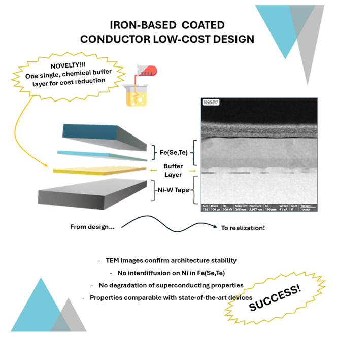
The design of iron-based coated conductors (IBS-CC) with a simplified architecture is possible thanks to the material properties that allow for milder requirements on the template crystalline quality. With respect to the state-of-the-art multilayered layout, it is possible to use a single buffer layer that remains necessary for protection and to promote the oriented growth of the superconducting film. In this work, Fe(Se,Te) films are grown via pulsed laser deposition (PLD) on commercial tapes using a single, chemically deposited, CeO2-based buffer layer, and interesting properties are obtained. In detail, the preparation and characterization of the buffer layer is presented, along with the detailed analysis of the Fe(Se,Te) current transport properties. The samples show superconducting transitions with Tc0 around 12 K and critical current densities of ∼0.1 MA cm−2 at 4.2 K at zero field. These results show that the design of a low-cost IBS-CC with a single chemical buffer layer is possible.
Subject areas: Physics, Materials science, Materials property
Graphical abstract
Highlights
-
•
Iron-based superconductors allow to simplify the coated-conductor architecture
-
•
Further cost-reduction is obtained with synthesis via chemical methods
-
•
The proposed design properties match the state-of-the-art iron-based devices
Physics; Materials science; Materials property
Introduction
In order to exploit superconductivity for large-scale power applications, conductors in the form of flexible wires or tapes are required. If high temperature superconductors (HTS) are used, such as REBCO materials (REBCO, rare-earth barium copper oxide), it is necessary to make up for their fragile and brittle nature by preparing them in the so-called coated conductor (CC) architecture. This technology is based on a complex multilayered structure of buffer layers and biaxially textured superconducting films on metallic substrates,1,2,3,4,5 to allow the exploitation of the extraordinary properties of these materials. However, such a complicated structure limits their potentiality for applications because of high production costs. In this scenario, any advancement that would lead to a simplification of the CC structure, could be a game-changer. A possibility could be to use superconductors with reduced sensitivity to the buffer layer’s grain orientation, and therefore to superconducting weak links, instead of REBCO. For example, iron-based superconductors (IBSCs) show larger critical current, Jc, tolerance to grain-to-grain misalignment (about 9° for Fe(Se,Te) with respect to 5° for REBCO materials) and structural disorder. In general, great interest was raised by these materials properties since their discovery in 20086 because of a peculiar combination of high critical temperature, Tc, high critical magnetic fields and Jc that makes them promising for a wide range of practical applications.7,8,9,10,11,12 Among IBSCs, iron chalcogenides drew significant attention due to their low toxicity and low structural anisotropy. Another property that makes Fe(Se,Te) extremely appealing notwithstanding the low critical temperatures – e.g., about 15 K for bulk Fe(Se,Te) – is the low deposition temperature (e.g., 200°C–400°C, in ultra-high vacuum conditions). These characteristics make the use of superconducting iron-chalcogenides such as Fe(Se,Te) instead of REBCO in the coated conductor extremely beneficial, since it would lead to a significant simplification of the CC architecture complexity and cost: from the complex buffer architecture necessary to obtain optimally textured REBCO films, to the 1–2 layers required for Fe(Se,Te),4,9,13,14 thanks to the high grain misalignment tolerance and low temperature processing. Several works have already shown that Fe(Se,Te) can be successfully obtained in form of tapes4,5,13,15,16,17,18 with the same technology developed and commercialized for HTS REBCO tapes, due to the similar lattice parameters. More in detail, the direct deposition on bare metallic substrates was not successful due to metallic contamination19 leading to suppression of superconductivity, but this phenomenon can be controlled, as for HTS tapes, with the use of a buffer layer.
As regards buffer layers, it was previously demonstrated that the extensively studied CeO2 is suitable for the preparation of high quality Fe(Se,Te), as it was for REBCO.20,21,22,23,24,25 Nowadays it is mainly grown on Ni-W substrates by pulsed laser deposition (PLD), however, the replacement of the expensive PLD with more cost-effective, chemical solution deposition (CSD) methods for the growth of the buffer13,26,27,28,29,30,31,32 would represent a relevant advancement toward low-cost IBS-CC. Therefore, it was proven that Zr-doped CeO2 (CZO) deposited via Metal Organic Decomposition (MOD) on YSZ single crystal substrates is an excellent buffer for high quality superconducting Fe(Se,Te) films.13,14
The aim of this study is to transfer the aforementioned results on commercial metallic tapes, and prove that the simplified architecture Ni-W/CZO-(MOD)/Fe(Se,Te) is suitable for the design and manufacturing of large scale iron-based CCs. We hereby give a detailed investigation of the structural and superconducting properties at high magnetic fields of Fe(Se,Te) films grown by PLD on CZO buffered Ni-W tapes. The final Fe(Se,Te) film displays promising superconducting performances, such as a Jcs.f. = 0.1 MA cm−2 at 4.2 K, and a Tc0 = 11.8 K. This work builds up on previously published studies,5,13,14,33 in which every element of the architecture was studied and tested, elucidating the role of the buffer layer on the final film properties and analyzing in detail the effect of the Fe(Se,Te) film structure on the transport properties of the superconductor. This work represents a relevant advancement toward low-cost IBS-CC: indeed, the union of Ni-W RABiTS (Rolling Assisted Biaxially Textured Substrates) tapes and the chemical deposition of the buffer layer allows for a significant reduction of the template costs, since these techniques are intrinsically vacuum-free given that they involve only thermomechanical treatments for the substrate and thermal treatments for the buffer, while other techniques such as IBAD (Ion beam Assisted Deposition) or ISD (Inclined Substrate Deposition) commonly employed for the template preparation are tied to vacuum systems.
Results and discussion
Buffer layer deposition and characterization
Zr-doped CeO2 buffer layers are grown via MOD on Ni-W metallic substrates. Regarding the MOD method, the well-established treatments13,14,27 yield high quality results with excellent reproducibility on Y-stabilized ZrO2 (YSZ) single crystal substrates. However, working with metallic tapes required the redefinition of the thermal treatment in order to obtain epitaxial, (00L)-oriented, flat films,26 without oxidizing the Ni-W tapes. A short thermal treatment under reducing conditions (15 min, 1100°C, Ar/H2, more details in the experimental section) was developed. In Figure 1 the XRD diffraction pattern and morphology of a CZO film grown on Ni-W via MOD is shown. The film is (00L) oriented, with a value of FWHMω-scan = 6.5°, comparable with that of the Ni-W substrate.5 The microstructure, investigated via AFM, shows large, flat grains (Figure S1, left panel). No holes can be seen, and the film appears continuous. When performing these analyses, few areas of the samples were found to have a very different morphology, in which the CZO flat grains are much smaller (Figure S1, right panel). This feature was more easily observed when looking at the samples via SEM at low magnification, as shown in Figure 1. Here, the right panel shows the boundary between an area with the flat morphology and one in which only smaller grains are visible; the right panel shows, at higher magnification, the area in which CZO grows with only flat-topped grains. When performing the EBSD analysis of these samples (Figure S2) the pole figures show a 45° in-plane rotation of the CZO lattice with respect to Ni-W, necessary to accommodate the differences in lattice parameters of the two materials. Moreover, it is found that the EBSD pattern of the flat-terraced regions is sharper with respect to those in which the rougher morphology is visible. Only a few of the rougher areas do not yield any pattern at all and are therefore polycrystalline. The origin of this behavior was analyzed in detail, by carefully mapping the Ni-W substrate and analyzing the same exact region after every step of the process, from buffer layer deposition to Fe(Se,Te) growth. The main finding is that grains in the Ni-W substrates that are slightly tilted and/or faceted result in grains of the CZO buffer with a not-optimal orientation and morphology. This, in consequence, causes the growth of polycrystalline grains in the Fe(Se,Te) films, as shown in the next section.
Figure 1.

XRD characterization of the CZO buffer layer
Left: XRD diffraction of a CZO film obtained via MOD. In the inset, w-scan of the CZO (200) peak; Right: SEM images at different magnifications of a CZO buffer deposited on Ni-W via MOD.
To evaluate the CZO film quality and effectiveness as a buffer layer, XPS measurements were performed to analyze the chemical composition of the CZO surface. Additionally, we subjected the CZO-buffered Ni-W to the same heat treatment used for the deposition of the Fe(Se,Te) seed layer to evaluate its robustness, as mentioned in the experimental section. In panel (a) of Figure 2, the survey spectra of the as-prepared and annealed sample are compared. As expected, they show the presence of the elements of the CZO buffer layer, and there is no noticeable difference between the spectra of the as-prepared and annealed states, emphasizing the robustness of the buffer layer to the necessary thermal treatments. Panel (b) displays the high-resolution spectrum in the 2p peak region of Ni, highlighting the absence of nickel on the buffer surface before and after the heat treatment. The absence of Ni from the surface is crucial, given its detrimental impact on the superconducting properties of the Fe(Se,Te) film.5 Panel (c) displays the high-resolution spectrum of the 4f region for the tungsten peak. Also in this case, there is no difference between the as-prepared and the annealed state, suggesting that the oxidation state of the tungsten is not influenced by the heat treatment necessary for the deposition of the Fe(Se,Te) layer. For the as-prepared state, the energy of the W 4f 7/2 (34.7 eV for the as-prepared and 34.8 for the annealed) and the W 4f 5/2 (36.8 eV for the as-prepared and 36.9 eV for the annealed) indicate the unexpected presence of a non-negligible amount of WO3.34 Additionally, mixed oxides NiWO4 can be excluded.35 The same WO3 was observed in a preliminary XPS analysis of the Ni-W bare substrate, and the high reactivity of Ce with W for the formation of a mixed oxide is well known,36 but its presence on the buffer surface is somewhat puzzling, due to the limited diffusion of W in CeO2.37,38 While the segregation of WO3 on the surface of Ni-W can be explained by the natural reactivity of a metallic surface exposed to air, we can only speculate that high-temperature diffusion at the grain boundary plays a significant role in its migration to the buffer surface. However, its presence does not interfere with the heteroepitaxial growth of the CZO buffer and the FST film (see next section). The high-resolution spectra of the Ce 3days region are shown in panel (d). As indicated for the other spectra, in this case, the chemical state of the buffer layer is not influenced by the heat treatment, highlighting once again the robustness of the buffer layer concerning thermal treatments. According to the energies of the peaks and with the analysis by Maslakov et al.,39 they can be ascribed to the CeO2 oxide. Finally, to prove the effectiveness of the buffer layer against Ni diffusion, high-resolution spectra of the Ni 2P region, shown in panel (b), were measured both in the as-prepared and annealed state. In both cases, the spectra show Ni absence on the buffer layer surface. Therefore, CZO can efficiently protect the Fe(Se,Te) film from Ni poisoning. Having thus established the optimal conditions for CZO buffer growth, the Fe(Se,Te) films are deposited via PLD.
Figure 2.

XPS characterization of the CZO buffer layer
(A) XPS spectrum of a CZO buffer layer on Ni-W, and details of the (B) Ni 2p, (C) W 4f, (D) Ce 3days regions of the spectrum.
Fe(Se,Te) structural characterization
XPS analysis was conducted on the as-deposited Fe(Se,Te) film to investigate the chemical composition of its surface. As shown from the survey spectra of Figure 3 panel (a), only the Fe, Se, and Te peaks can be recognized (alongside the oxygen and carbon peaks coming from atmospheric contamination). To confirm the absence of nickel on the surface of the Fe(Se,Te) film, high-resolution spectra of the Ni 2P region were measured. As evident from these measurements, the absence of Ni from the film surface is shown, validating the effectiveness of the single CZO buffer layer as a diffusion barrier for nickel. Additionally, high-resolution spectra were measured for the W 4f region to ensure no diffusion of tungsten atoms from the surface layer of the CZO layer through the film. The results presented in panel (c) confirm the absence of W contamination in the surface layer of the Fe(Se,Te).
Figure 3.

XPS characterization of the Fe(Se,Te) film
(A) XPS spectrum of a Fe(Se,Te) film deposited on an MOD CZO buffered NiW, and details of the (B) Ni 2p, (C) W 4f regions of the spectrum.
In Figure 4 left panel, the XRD θ–2θ diffraction pattern of a Fe(Se,Te) film deposited on CZO-buffered Ni-W is shown. The intense (00L) Fe(Se,Te) reflections are visible, as well as signals belonging to both the CZO buffer and the Ni-W substrate. In Figure 4, the Fe(Se,Te) (001) peak is split in two components, as highlighted in the inset: this feature is related to the superconducting film deposition process, that involves the low temperature deposition of a superconducting layer on top of a seed layer grown at higher temperatures. The higher temperatures used for the seed layer are necessary to facilitate heteroepitaxial growth on the buffer, at the expense of superconducting properties that are suppressed due to a higher Se:Te ratio in the seed layer. Subsequently, homoepitaxial growth of the superconducting top layer is carried out at lower temperatures. This difference in deposition temperatures (400°C for the seed and 200°C for the top layer) strongly influences the stoichiometry of the growing Fe(Se,Te), that causes a significant difference in lattice parameters between the seed layer and the top layer and, therefore, of the relative XRD reflection position. Further details on the seed+top layer Fe(Se,Te) structure topic can be found in.33,40 In synthesis, the use of the seed layer has advantageous effects on the growth of the superconductive layer, facilitating crystal and chemical compatibility between the substrate and the superconducting film through homoepitaxial growth, hence ensuring higher quality and reproducibility of the superconductive Fe(Se,Te) layer. Regarding film epitaxy, the Fe(Se,Te) top layer shows optimal out-of-plane orientation, with a (001) ω-scan FWHM = 7.4°, value close to that of the seed layer which shows a slightly narrower distribution (FWHM = 6.5°). These values are comparable and consistent with what measured for the buffer layer and the Ni-W substrate, and it should be stressed how the orientation is retained from the metallic substrate to the top layer.
Figure 4.

XRD characterization of the Fe(Se,Te) film
Left: XRD diffraction of a Fe(Se,Te) film deposited on an MOD CZO buffered Ni-W; the indicated peaks are to be referred to Fe(Se,Te) if not otherwise stated. In the inset, the highlight of the Fe(Se,Te) (001) peak splitting. Right: SEM images of a Fe(Se,Te) film deposited on an MOD CZO buffer at different magnifications.
Microstructural analyses of the sample surface were carried out via scanning electron microscopy (SEM), and EBSD, as previously done with the CZO buffer. Fe(Se,Te) shows a 45° rotation with respect to CZO, thus reflecting the Ni-W orientation. Figure 4, right panel shows the SEM images of a Fe(Se,Te) film deposited on CZO-(MOD) buffered Ni-W at different magnifications. At high magnifications, the surface appears very flat and crack-free, with few small misoriented grains. However, some regions can be identified where the number of misoriented grains clearly increases with respect to the rest of the sample. The EBSD analysis of these regions reveals that they correspond to single Fe(Se,Te) grains where the film is not oriented (no EBSD pattern recorded), as shown in Figure S3. As already mentioned, the correlative analysis of the EBSD pattern finds out that the polycrystalline Fe(Se,Te) grains correspond to the not-optimally-oriented CZO buffer grains grown on tilted Ni-W grains.
Microstructural characterization of this proposed coated conductor architecture is taken further with TEM imaging. In Figure 5, the TEM images of a cross section Fe(Se,Te) deposited on a CZO-(MOD) buffered Ni-W are shown. In the HAADF (High-Annular Angular Dark Field) image we can see (from the bottom): the Ni-W substrate, the CZO buffer layer and the Fe(Se,Te) film divided in seed layer (60 nm) and top layer, ∼150 nm thick. A highlight on the seed layer, Figure 5 central panel, shows how it grows with some slightly misoriented grains. Furthermore, the interface between the top and the seed layer, right panel, is smooth and seamless with limited structural disorder. The elemental analysis was also performed on the section, and Figure 6 highlights the homogeneous distribution of Fe between the two Fe(Se,Te) layers, whereas different distributions of the Se and Te signals are detected. This difference is, as previously explained for the XRD signals, a consequence of the different deposition temperatures between seed and top layer. A detailed discussion on this can be found in.33 As regards the buffer layer, no significant diffusion of Ce/Zr atoms is detected in the uppermost layers, and most importantly, no Ni seems to have diffused in the Fe(Se,Te), thus confirming the efficiency of the CZO buffer in its protective role toward Fe(Se,Te) poisoning from the substrate. It should be noticed, however, that the EDX analysis reveals a significant presence of Fe at the interface between CZO and Ni-W, and W in the CZO layer (Figure 7). As regards tungsten, its presence is in accordance with what was already observed via XPS on the surface of the buffer, that is, presence of WO3. We can argue that at high temperature the formation of Ce and W mixed oxides occurs, that causes the diffusion of W in the CZO layer: indeed, formation of such oxides was observed also under reducing atmospheres.41 Surprisingly, at the interface between Ni and CZO, a thin layer (2–3 nm, red arrow in Figure 7) can be identified that from the EDX analysis results mainly composed of Fe and Ni. This phenomenon is still under investigation, but a tentative explanation could be represented by the diffusion of Fe through grain boundaries and/or microcracks for the formation of Ni-Fe or Ni-Fe-W intermetallic compounds.
Figure 5.

TEM images of the cross section of a Fe(Se,Te) film grown on a CZO buffered Ni-W substrate
(A) low magnification image showing the layers of the CC architecture; (B) higher magnification image showing the seed layer growing with slightly misoriented grains, dashed lines indicate grain boundaries; (C) highlight on the seed/top layer interface showing small areas of structural disorder.
Figure 6.

TEM image of the cross section of a Fe(Se,Te) film grown on a CZO buffered Ni-W substrate with EDX analyses showing the distributions of Se, Te, Fe, Ce and Ni in the whole CC architecture
Figure 7.

TEM image of the cross section of a Fe(Se,Te) film grown on a CZO buffered Ni-W substrate: focus on the CZO buffer layer with EDX analyses showing Fe and W in the buffer layer
A. Fe(Se,Te) transport properties
The electrical characterization was carried out with the standard four probe method. The R vs. T behavior (Figure 8) reveals a superconducting transition at slightly lower temperatures with respect to previous results obtained for similar systems,33 with Tc0 = 11.8 K. This difference can be explained taking into account the substrate used for deposition: YSZ single crystals, in the mentioned papers, and Ni-W tape in this work. However, it is undoubtedly true that the proposed deposition process leaves room for further optimization that could reduce the difference in Tc0 with respect to the Fe(Se,Te) on single crystal. Moreover, in Figure 8, before the transition to zero resistance, an increase in R is observed. This behavior, already observed in similar systems,5,42 is common to all the superconducting Fe(Se,Te) samples on Ni-W prepared until now, and it can be ascribed to the presence of the metallic substrate associated to a significant inhomogeneity of the films that causes a current redistribution in the sample before transition.43 The sample was then patterned to undergo transport measurements. In Figure 8, left panel, also the R vs. T measurement of the patterned strip is shown. Here, the 3 K drop in Tc0 with respect to the whole film confirms the hypothesis of inhomogeneity even though some damage occurred during patterning cannot be ruled out. On the right, the Jc vs. field curves at different temperatures (4, 6 and 8 K) are shown. At 4 K the Jcsf is 0.1 MA/cm2, then it rapidly decreases with increasing field. The same rapid decrease is observed at the other temperatures. In Figure 9, left panel, the comparison with the Jc curves at 4 K for an FST film on PLD deposited CeO2 is shown (data from5). The two films show comparable Jc values at self-field, but a very different Jc vs. field behavior, with a much steeper decrease at low field for the FST/CeO2-(PLD)/Ni-W sample. A crossover around 3 T between the curves is visible, beyond which the FST/CZO-(MOD)/Ni-W film quickly reaches the irreversibility field. This difference in the in-field behavior can only partially be ascribed to very different Tc0s between the two films, 16 K for the FST/CeO2-(PLD)/Ni-W sample, and 8 K for the FST/CZO-(MOD)/Ni-W. In fact, not only there is a difference in Jc absolute values, but the whole Jc dependence on magnetic field is different, suggesting the existence of different Jc -limiting mechanisms. It is now common knowledge that the Jc behavior at low field is strongly related to the presence of weak links and, therefore, to the film microstructure and grain boundary distribution. Large angle grain boundaries limit the transmission of the supercurrent, leading to an exponential decay of Jc at low field, which is exactly what happens in the FST/CeO2-(PLD)/Ni-W sample. For the FST/CZO-(MOD)/Ni-W sample, instead, the Jc decay at low field is almost linear, resembling that of an FST film grown on buffered single crystal, as observed in33 in which no limitation related to large angle grain boundaries can be invoked due to the high film texture degree. This similarity is strongly evidenced in Figure 9, right panel, where the normalized current vs. field curves for the mentioned samples are compared to that of a Fe(Se,Te) film grown on a buffered single crystal, referred to as FST/CZO-(MOD)/YSZ. It is clearly visible how the FST/CZO-(MOD)/Ni-W is perfectly superimposed with the FST/CZO-(MOD)/YSZ film in the low field region, that could imply a microstructural similarity between the two samples related to the kind of grain boundaries present in the Fe(Se,Te) films. If we take another look at the grain boundary distribution presented in Figure S3, the maximum value of grain misalignment for the FST/CZO-(MOD)/Ni-W film is 9° (with the distribution peak at 3°), whereas for the FST/CeO2-(PLD)/Ni-W sample is 11° (with the distribution peak at 3°, see Figure S4). Given that for Fe(Se,Te) the critical angle is around 8°, we can reasonably guess that the lack of weak links in the FST/CZO-(MOD)/Ni-W samples causes the in-field behavior for this sample to be more similar to the FST/CZO-(MOD)/YSZ sample. Apart from the in-field behavior, that leaves room for improvement, the important conclusion is that the FST film on a chemical CZO buffer performs (in the low T, low H region) as well as an FST film on a PLD CeO2 buffer. This means that the proposed simplified architecture for IBS-CCs works, and that we can successfully switch from PLD to CSD for the buffer layer growth, with all the advantages of the process simplification and lower production costs. Further optimization of the system is in progress, starting from the deposition process of the superconductor itself, the evaluation of higher buffer thicknesses and the use of other phases as buffer layers, to avoid the problem of ion diffusion into the Fe(Se,Te).
Figure 8.

Electric characterization of the Fe(Se,Te) film on a MOD CZO-buffered Ni-W tape
Left: resistive transition, Right: Jc vs. field curves at 4, 6, and 8 K.
Figure 9.

Comparison of transport properties between a Fe(Se,Te) film on a MOD CZO-buffered Ni-W tape and an a Fe(Se,Te) film on a PLD CZO-buffered Ni-W tape
Left: Jc vs. field curves for the Fe(Se,Te) film on an MOD CZO-buffered Ni-W tape (black diamonds) compared with a Fe(Se,Te) film on a PLD CZO-buffered Ni-W tape (empty squares); Right: normalized Jc vs. field curves for the Fe(Se,Te) film on an MOD CZO-buffered Ni-W (black diamonds) tape compared with a Fe(Se,Te) film on a PLD CZO-buffered Ni-W tape (empty squares) and a Fe(Se,Te) film on an MOD CZO-buffered YSZ single crystal (black crosses).
Conclusions
This paper reports on the deposition and epitaxial growth of Fe(Se,Te) superconducting films on a chemically derived Zr-doped CeO2 buffer layer on commercial Ni-W tapes. The aim of this study is also to investigate the feasibility of an IBS-CC with a simplified architecture that requires only one buffer layer. Thus, we present a detailed characterization of the elements of the CC from the buffer to the final film structural and superconducting properties.
The chemical solution deposition method MOD was successfully employed to deposit CZO on Ni-W with a thermal treatment developed ad hoc, and the quality of the obtained buffers was assessed via evaluation of structural and microstructural parameters. Deposition of the Fe(Se,Te) film/seed layer was performed via PLD. The heteroepitaxial growth was successful, and the optimal structure was retained from the buffer to the top layer. A detailed TEM analysis shows how the buffer layer can effectively protect the Fe(Se,Te) film from Ni poisoning from the substrate, but also that grain boundary diffusion of W and Fe occurs during treatment. However, this has no influence on the epitaxial growth of the multilayer. Superconducting properties of a Fe(Se,Te) film deposited on CZO-(MOD) buffered Ni-W were evaluated via dc measurements and self-field performances resulted in line with data from the literature. Most importantly, they are comparable to the FST/CZO-(PLD)/Ni-W presented in,5 which means that MOD can successfully substitute PLD in the production process of an IBS-CC.
Resource availability
Lead contact
Further information and requests for resources should be directed to and will be fulfilled by the lead contact, Dr. Laura Piperno (laura.piperno@uniroma3.it).
Materials availability
The study did not generate new unique materials. The readers can buy the chemicals to remake the materials as mentioned in the text.
Data and code availability
-
•
Data: All data reported in this paper will be shared by the lead contact upon request.
-
•
Code: This paper does not report the original code. Any additional information required to reanalyze the data reported in this paper is available from the lead contact upon request.
Acknowledgments
This work has been carried out within the framework of the EUROfusion Consortium, funded by the European Union via the Euratom Research and Training Programme (Grant Agreement No 101052200 — EUROfusion). Views and opinions expressed are however those of the author(s) only and do not necessarily reflect those of the European Union or the European Commission. Neither the European Union nor the European Commission can be held responsible for them.
This work was also partially supported by MIUR-PRIN project ‘HiBiSCUS’—Grant No. 201785KWLE.
Author contributions
Conceptualization, L.P., A.V., G.C., V.B., M.C., and M.I.; Investigation, L.P., A.V., F.R., A.M., A.R., G.C., V.B., M.C., L.S., A.M., and M.I.; Writing – Original Draft, L.P.; Writing – Revision, L.P., A.V., F.R., A.M., A.R., G.C., V.B., M.C., L.S., M.I., G.S. and M.P.; Supervision, G.C., G.S., and M.P.; Project Administration and Funding Acquisition, G.C., M.P., and L.P.
Declaration of interests
The authors have no conflicts of interest to declare.
STAR★Methods
Key resources table
| REAGENT or RESOURCE | SOURCE | IDENTIFIER |
|---|---|---|
| Chemicals, peptides, and recombinant proteins | ||
| Ce(III) acetate hydrate 99.5% | Sigma Aldrich | |
| Zr (IV) acetylacetonate 98% | Sigma Aldrich | |
| Propionic Acid 98% | Sigma Aldrich | |
| Ni-5 at % W Tapes | GmbH | |
| Software and algorithms | ||
| Gwyddion | http://gwyddion.net/ | |
Experimental model and study participant details
This study does not use experimental models.
Method details
Sample preparation
MOD Buffer layers
MOD Zr-doped CeO2 (CZO) precursor solution was prepared dissolving stoichiometric amounts of Ce (III) acetate hydrate (Sigma Aldrich, 99.5%) and 5 mol.% Zr (IV) acetylacetonate (Sigma Aldrich, 98%) in propionic acid (Sigma Aldrich, 99.5%). Rotary evaporation was used to remove water and the excess of solvent until a total metal concentration [Ce] + [Zr] = 0.3 M is obtained. The solution was deposited on 1×1 cm2 Ni-5 at % W (Ni-W) biaxially textured substrate (GmbH) by spin coating at 2000 rpm for 60 s. The thermal treatment was carried out in flowing 5% Ar-H2 (0.5 l/min Ar-H2) at 1150°C for 15 min (ramps 10°C/min). Films approximately 30 nm thick are thus obtained.
PLD Fe(Se,Te) films
Fe(Se,Te) films were deposited by pulsed laser deposition (PLD) in an ultra-high vacuum chamber (residual gas pressure during deposition of about 10–8 mbar during deposition) equipped with a Nd:YAG laser at 1064 nm and using a polycrystalline target with a nominal composition FeSe0.5Te0.5 synthesized using a two-step method.7 First, a non-superconducting seed layer of about 50 nm was deposited at 400°C at high laser repetition rate (10 Hz). Then, the sample was cooled to 200°C for 150 nm top-layer deposition at 3 Hz. The films were deposited keeping the following parameters: 2 J cm−2 laser fluency (2 mm2 spot size) and a 5 cm distance between target and sample. The use of the seed layer was shown to be necessary to optimize the film properties.33
Sample characterization
Structural characterization was carried out by X-ray diffraction (XRD) using a Rigaku GeigerFlex diffractometer equipped with a Cu-radiation source and a monochromator on the diffracted beam in Bragg–Brentano configuration for both θ–2θ and ω-scans. ω-scans were fitted using a pseudo-Voigt curve to obtain the full width at half maximum (FWHM) values.
AFM measurements were performed on a Park Systems XE-150 atomic force microscope operating in non-contact mode at room temperature. Image analysis was performed using the open source Gwyddion software as in.5,13,14
XPS analysis was performed in a dedicated ultra high vacuum chamber equipped with a hemispherical energy analyzer (model 10-360) and a monochromatic X-ray source (model 10-610) by Physical Electronics. The base pressure of the system is lower than 5×10⁻⁸ mbar. All the XPS spectra reported in this work were acquired using a monochromatized Al-Ka X-ray source (photon energy hv=1486.6 eV); the spot was approximately 100 μm in diameter and the photoemitted electrons were collected at an emission angle of 45° from the surface normal. The binding energy was calibrated by fixing the C 1s line at 284.40 eV (corresponding to adventitious carbon). In all regions, the peaks position was determined by fitting them with a Doniach Sunjic function, after subtracting a Shirley background. All the analyses on the spectra were performed using the Fityk software.44 Peak identification was performed based on the NIST X-ray Photoelectron Spectroscopy Database (https://srdata.nist.gov/xps/ accessed 5/12/2023).
CZO buffer layers on Ni-W were measured both at 300 K and after an annealing procedure (from 300 to 500 K at 8 Kmin-1 plus a dwell at 773 K for 15 minutes, P < 5×10⁻⁷ mbar); if necessary, the spectra were vertically shifted for sake of clarity. A LEO 1525 field emission high-resolution Scanning Electron Microscope (SEM), equipped with Oxford x-act EDX system and a Nordlys Nano electron backscattering diffraction (EBSD) system, was used to investigate the surface morphology, elemental composition and sample microstructure.
For TEM measurements, cross section lamellas were produced by focused ion beam. STEM EDX mappings were carried out on a Thermofisher Spectra Ultra operated at 200 kV, equipped with a Ultra-X EDX detector operated at 200 kV.
The electrical resistance as a function of the temperature was measured in dc in a liquid He cryostat by the four-probe method. The critical temperature Tc0 was evaluated as zero-resistance temperature.14
Critical current measurements and in-field R(T) measurements were carried out on strips with defined geometry obtained after patterning with optical photolithographic procedures in a cryo-free cryostat equipped with an 18 T superconducting magnet. The strip width used for this study is 500 μm. Critical current is defined with the electric field threshold Ec = 1 μVcm-1.
Quantification and statistical analysis
This study does not include statistical analysis or quantification.
Published: September 26, 2024
Footnotes
Supplemental information can be found online at https://doi.org/10.1016/j.isci.2024.111032.
Supplemental information
References
- 1.Huang J., Chen L., Jian J., Khatkhatay F., Jacob C., Wang H. A simplified superconducting coated conductor design with Fe-based superconductors on glass and flexible metallic substrates. J. Alloys Compd. 2015;647:380–385. doi: 10.1016/J.JALLCOM.2015.06.109. [DOI] [Google Scholar]
- 2.Si W., Han S.J., Shi X., Ehrlich S.N., Jaroszynski J., Goyal A., Li Q. High current superconductivity in FeSe 0.5 Te 0.5-coated conductors at 30 tesla. Nat. Commun. 2013;4:1347. doi: 10.1038/ncomms2337. [DOI] [PubMed] [Google Scholar]
- 3.Fan F., Zhang X., Cai C., Ma Y. Angular dependence of the critical current density in FeSe0.5 Te0.5 thin films on metal substrates. Supercond. Sci. Technol. 2021;34 doi: 10.1088/1361-6668/ac2e5c. [DOI] [Google Scholar]
- 4.Sakoda M., Iida K., Naito M. IOP Publishing; 2018. Recent Progress in Thin-Film Growth of Fe-Based Superconductors: Superior Superconductivity Achieved by Thin Films. [DOI] [Google Scholar]
- 5.Sylva G., Augieri A., Mancini A., Rufoloni A., Vannozzi A., Celentano G., Bellingeri E., Ferdeghini C., Putti M., Braccini V. Fe(Se,Te) coated conductors deposited on simple rolling-assisted biaxially textured substrate templates. Supercond. Sci. Technol. 2019;32 doi: 10.1088/1361-6668/ab0e98. [DOI] [Google Scholar]
- 6.Kamihara Y., Watanabe T., Hirano M., Hosono H. Iron-based layered superconductor La[O1-xFx]FeAs (x= 0.05-0.12) with Tc = 26 K. J. Am. Chem. Soc. 2008;130:3296–3297. doi: 10.1021/JA800073M. [DOI] [PubMed] [Google Scholar]
- 7.Palenzona A., Sala A., Bernini C., Braccini V., Cimberle M.R., Ferdeghini C., Lamura G., Martinelli A., Pallecchi I., Romano G., et al. A new approach for improving global critical current density in Fe(Se0.5Te0.5) polycrystalline materials. Supercond. Sci. Technol. 2012;25 doi: 10.1088/0953-2048/25/11/115018. [DOI] [Google Scholar]
- 8.Bruzzone P., Fietz W.H., Minervini J.V., Novikov M., Yanagi N., Zhai Y., Zheng J. High temperature superconductors for fusion magnets. Nucl. Fusion. 2018;58 doi: 10.1088/1741-4326/aad835. [DOI] [Google Scholar]
- 9.Hosono H., Yamamoto A., Hiramatsu H., Ma Y. Recent advances in iron-based superconductors toward applications. Mater. Today. 2018;21:278–302. doi: 10.1016/j.mattod.2017.09.006. [DOI] [Google Scholar]
- 10.Pallecchi I., Eisterer M., Malagoli A., Putti M. Application potential of Fe-based superconductors. Supercond. Sci. Technol. 2015;28:114005. doi: 10.1088/0953-2048/28/11/114005. [DOI] [Google Scholar]
- 11.Whyte D.G., Minervini J., Labombard B., Marmar E., Bromberg L., Greenwald M. Smaller & Sooner: Exploiting High Magnetic Fields from New Superconductors for a More Attractive Fusion Energy Development Path. J. Fusion Energy. 2016;35:41–53. doi: 10.1007/s10894-015-0050-1. [DOI] [Google Scholar]
- 12.Torsello D., Gerbaldo R., Gozzelino L., Laviano F., Takahashi A., Park A., Pyon S., Ichinose A., Tamegai T., Ghigo G. Twofold role of columnar defects in iron based superconductors. Supercond. Sci. Technol. 2020;33 doi: 10.1088/1361-6668/ABA350. [DOI] [Google Scholar]
- 13.Vannozzi A., Prili S., Sylva G., Masi A., Armenio A.A., Mancini A., Pinto V., Rufoloni A., Piperno L., Augieri A., et al. Epitaxial Zr-doped CeO2films by chemical solution deposition as buffer layers for Fe(Se,Te) film growth. Supercond. Sci. Technol. 2020;33 doi: 10.1088/1361-6668/ab9aa7. [DOI] [Google Scholar]
- 14.Piperno L., Vannozzi A., Pinto V., Augieri A., Armenio A.A., Rizzo F., Mancini A., Rufoloni A., Celentano G., Braccini V., et al. Chemical CeO2-based buffer layers for Fe(Se,Te) films. IEEE Trans. Appl. Supercond. 2022;32:1–5. doi: 10.1109/TASC.2022.3142709. [DOI] [Google Scholar]
- 15.Hänisch J., Iida K., Hühne R., Tarantini C. Institute of Physics Publishing; 2019. Fe-based Superconducting Thin Films-Preparation and Tuning of Superconducting Properties. [DOI] [Google Scholar]
- 16.Sebastian M.A.P., Reichart J.N., Ratcliff M.M., Bullard T.J., Burke J.L., Ebbing C.R., Panasyuk G.Y., Tsai C.-F., Zhang W., Huang J., et al. Study of the flux pinning landscape of YBCO thin films with single and mixed phase additions BaMO3+ Z: M= Hf, Sn, Zr and Z= Y2O3, Y211. IEEE Trans. Appl. Supercond. 2017;27:1–5. [Google Scholar]
- 17.Anna Thomas A., Shipulin I.A., Holleis S., Eisterer M., Nielsch K., Hühne R. Comparative study of Fe(Se,Te) thin films on flexible coated conductor templates and single-crystal substrates. Supercond. Sci. Technol. 2021;34 doi: 10.1088/1361-6668/AC2557. [DOI] [Google Scholar]
- 18.Torsello D., Fracasso M., Gerbaldo R., Ghigo G., Laviano F., Napolitano A., Iebole M., Cialone M., Manca N., Martinelli A., et al. Proton Irradiation Effects on the Superconducting Properties of Fe(Se,Te) Thin Films. IEEE Trans. Appl. Supercond. 2022;32:1–5. doi: 10.1109/TASC.2021.3136135. [DOI] [Google Scholar]
- 19.Sylva G., Malagoli A., Bellingeri E., Putti M., Ferdeghini C., Vannozzi A., Celentano G., Hopkins S.C., Lunt A., Ballarino A., Braccini V. Analysis of Fe(Se,Te) films deposited on unbuffered invar 36. IEEE Trans. Appl. Supercond. 2019;29:1–5. doi: 10.1109/TASC.2019.2893585. [DOI] [Google Scholar]
- 20.Cavallaro A., Sandiumenge F., Gàzquez J., Puig T., Obradors X., Arbiol J., Freyhardt H.C. Growth mechanism, microstructure, and surface modification of nanostructured CeO2 films by chemical solution deposition. Adv. Funct. Mater. 2006;16:1363–1372. doi: 10.1002/adfm.200500206. [DOI] [Google Scholar]
- 21.Obradors X., Puig T. Coated conductors for power applications: materials challenges. Supercond. Sci. Technol. 2014;27 doi: 10.1088/0953-2048/27/4/044003. [DOI] [Google Scholar]
- 22.Paranthaman M.P., Sathyamurthy S., Bhuiyan M.S., Goyal A., Kodenkandath T., Li X., Zhang W., Thieme C.L.H., Schoop U., Verebelyi D.T., Rupich M. Improved YBCO coated conductors using alternate buffer architectures. IEEE Trans. Appl. Supercond. 2005;15:2632–2634. doi: 10.1109/TASC.2005.847686. [DOI] [Google Scholar]
- 23.Albiss B.A., Obaidat I.M. Applications of YBCO-coated conductors: a focus on the chemical solution deposition method. J. Mater. Chem. 2010;20:1836–1845. [Google Scholar]
- 24.Coll M., Gázquez J., Hühne R., Holzapfel B., Morilla Y., García-López J., Pomar A., Sandiumenge F., Puig T., Obradors X. All chemical YBa2Cu307 superconducting multilayers: Critical role of CeO2 cap layer flatness. J. Mater. Res. 2009;24:1446–1455. doi: 10.1557/jmr.2009.0160. [DOI] [Google Scholar]
- 25.Pop C., Villarejo B., Pino F., Mundet B., Ricart S., De Palau M., Puig T., Obradors X. Growth of all-chemical high critical current YBa2 Cu3 O7-δ thick films and coated conductors. Supercond. Sci. Technol. 2019;32 doi: 10.1088/1361-6668/aaea4e. [DOI] [Google Scholar]
- 26.Piperno L., Vannozzi A., Sotgiu G., Celentano G. CeO2-based buffer layers via chemical solution deposition: Critical issues and latest developments. J. Eur. Ceram. Soc. 2021;41:2193–2206. doi: 10.1016/j.jeurceramsoc.2020.11.016. [DOI] [Google Scholar]
- 27.Campagna E., Piperno L., Pinto V., Augieri A., Rufoloni A., Mancini A., Angrisani Armenio A., Masi A., Rizzo F., Salvato M., et al. All-chemical YBCO-based architecture using a sim-plified multilayer buffer deposition. IEEE Trans. Appl. Supercond. 2022;32:1–5. [Google Scholar]
- 28.Pinto V., Angrisani Armenio A., Piperno L., Mancini A., Rizzo F., Vannozzi A., Rufoloni A., Augieri A., Galluzzi V., Frolova A., et al. Aging of precursor solutions used for YBCO films chemical solution deposition: Study of mechanisms and effects on film properties. IEEE Trans. Appl. Supercond. 2016;26:1–5. doi: 10.1109/TASC.2016.2542587. [DOI] [Google Scholar]
- 29.Pinto V., Lamanna R., Vannozzi A., Angrisani Armenio A., De Marzi G., Augieri A., Piperno L., Sotgiu G., Celentano G. Solution Refining for MOD-YBCO Optimization: An NMR Study. IEEE Trans. Appl. Supercond. 2018;28:1–5. doi: 10.1109/TASC.2018.2800767. [DOI] [Google Scholar]
- 30.Santoni A., Rondino F., Piperno L., Armenio Angrisani A., Pinto V., Mancini A., Augieri A., Frolova A., Rufoloni A., Vannozzi A., et al. Zirconium distribution in solution-derived BaZrO3 - YBa2Cu3O7-δ epitaxial thin films studied by X-ray photoelectron spectroscopy. Thin Solid Films. 2019;669:531–536. doi: 10.1016/j.tsf.2018.11.054. [DOI] [Google Scholar]
- 31.Piperno L., Rasi S., De Santis S., Masi A., Santoni A., Mancini A., Angrisani Armenio A., Pinto V., Farjas J., Sotgiu G., Celentano G. Elucidation of the decomposition reactions of low-fluorine YBa2Cu3O7-x precursors during film pyrolysis. J. Anal. Appl. Pyrolysis. 2020;148 doi: 10.1016/j.jaap.2020.104777. [DOI] [Google Scholar]
- 32.Piperno L., Vannozzi A., Pinto V., Angrisani Armenio A., Rondino F., Santoni A., Mancini A., Rufoloni A., Augieri A., Tortora L., et al. Interaction between untreated SrTiO3 substrates and solution-derived YBa2Cu3O7-δ films. Appl. Surf. Sci. 2020;528 doi: 10.1016/j.apsusc.2020.146402. [DOI] [Google Scholar]
- 33.Piperno L., Vannozzi A., Augieri A., Masi A., Mancini A., Rufoloni A., Celentano G., Braccini V., Cialone M., Iebole M., et al. High-performance Fe(Se,Te) films on chemical CeO2-based buffer layers. Sci. Rep. 2023;13:569. doi: 10.1038/s41598-022-24044-5. [DOI] [PMC free article] [PubMed] [Google Scholar]
- 34.Shi J., Allara D.L. Characterization of High-Temperature Reactions at the BaO/W Interface. Langmuir. 1996;12:5099–5108. doi: 10.1021/LA960196. [DOI] [Google Scholar]
- 35.Salvati L., Makovsky L.E., Stencel J.M., Brown F.R., Hercules D.M. Surface spectroscopic study of tungsten-alumina catalysts using X-ray photoelectron, ion scattering, and Raman spectroscopies. J. Phys. Chem. 1981;85:3700–3707. doi: 10.1021/J150624A035. [DOI] [Google Scholar]
- 36.Skála T., Matolín V. Model thin films of Ce(III)-based mixed oxides. Surf. Interface Anal. 2014;46:993–996. doi: 10.1002/SIA.5458. [DOI] [Google Scholar]
- 37.Skála T., Tsud N., Prince K.C., Matolín V. Interaction of tungsten with CeO2(111) layers as a function of temperature: a photoelectron spectroscopy study. J. Phys. Condens. Matter. 2011;23 doi: 10.1088/0953-8984/23/21/215001. [DOI] [PubMed] [Google Scholar]
- 38.Polyak Y., Bastl Z. XPS and factor analysis study of initial stages of cerium oxide growth on polycrystalline tungsten. Surf. Interface Anal. 2015;47:663–671. doi: 10.1002/SIA.5762. [DOI] [Google Scholar]
- 39.Maslakov K.I., Teterin Y.A., Popel A.J., Teterin A.Y., Ivanov K.E., Kalmykov S.N., Petrov V.G., Petrov P.K., Farnan I. XPS study of ion irradiated and unirradiated CeO2 bulk and thin film samples. Appl. Surf. Sci. 2018;448:154–162. doi: 10.1016/J.APSUSC.2018.04.077. [DOI] [Google Scholar]
- 40.Molatta S., Haindl S., Trommler S., Schulze M., Wurmehl S., Hühne R. Interface control by homoepitaxial growth in pulsed laser deposited iron chalcogenide thin films. Sci. Rep. 2015;5:16334. doi: 10.1038/srep16334. [DOI] [PMC free article] [PubMed] [Google Scholar]
- 41.Yoshimura M., Sibieude F., Rouanet A., Foex M. Identification of binary compounds in the system Ce2O3-WO3. J. Solid State Chem. 1976;16:219–232. doi: 10.1016/0022-4596(76)90037-2. [DOI] [Google Scholar]
- 42.Mancini A., Armenio A.A., Celentano G., Piperno L., Rufoloni A., Masi A., Vannozzi A. Study of seed layer growth for superconducting Fe(Se,Te) film deposition. IEEE Trans. Appl. Supercond. 2023;34:1–5. doi: 10.1109/TASC.2023.3338598. [DOI] [Google Scholar]
- 43.Vaglio R., Attanasio C., Maritato L., Ruosi A. Explanation of the resistance-peak anomaly in nonhomogeneous superconductors. Phys. Rev. B. 1993;47:15302–15303. doi: 10.1103/PhysRevB.47.15302. [DOI] [PubMed] [Google Scholar]
- 44.Wojdyr M. Fityk: a general-purpose peak fitting program. J. Appl. Crystallogr. 2010;43:1126–1128. doi: 10.1107/S0021889810030499. [DOI] [Google Scholar]
Associated Data
This section collects any data citations, data availability statements, or supplementary materials included in this article.
Supplementary Materials
Data Availability Statement
-
•
Data: All data reported in this paper will be shared by the lead contact upon request.
-
•
Code: This paper does not report the original code. Any additional information required to reanalyze the data reported in this paper is available from the lead contact upon request.