Abstract
In this work, we synthesized SnS and MnSe compositions using a hydrothermal method and then prepared the SnS/MnSe heterostructure. By using X-ray diffraction, the structural characteristics of these compounds were examined. It was discovered that both the pure phases MnSe and SnS appeared in the SnS/MnSe sample, confirming the heterostructure formation. The Raman analysis also confirmed the formation of a heterostructure of the SnS/MnSe sample containing two phases, MnSe and SnS. The individual MnSe and SnS compositions show good optical properties, having bandgap values around 1.3 and 1 eV, respectively, whereas the prepared heterostructure shows a very low bandgap value of around 0.4 eV. The SnS sample shows nano sheet-like morphology, and MnSe shows rectangular-like shapes, whereas the SnS/MnSe heterostructure shows the presence of both shapes. The EDX study shows all the constituent elements in the SnS/MnSe heterostructure sample. The electrical study also shows that the properties of the prepared heterostructure are different from those of pure compositions. Investigating the dielectric characteristics with respect to temperature and frequency allowed for a thorough analysis of several parameters, including the electric modulus, dielectric constant, AC conductivity, and impedance spectroscopy. Applications for electronic and energy storage devices may benefit from the aforementioned optical, electrical, and dielectric characteristics of the SnS/MnSe heterostructure.
We report the synthesis of the SnS/MnSe heterostructure which shows a low bandgap of 0.4 eV with good electrical and dielectric properties useful for optoelectronics and dielectric applications.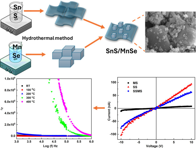
1. Introduction
Over the past ten years, nanotechnology has developed at a faster rate and has been effectively used for real-world applications. Nanomaterials with a controlled shape have drawn the attention of several researchers, specifically one-dimensional nanostructures in the solution-phase. Group IV–VI elements, including Ge, Sn, Se, Pb, and Te, have smaller band gaps. Since such materials exhibit near-infrared and infrared optical activity, they are now the subject of intensive research. Materials based on tin chalcogenides, such as tin sulfide (SnS), having semiconducting properties, have become extremely popular because of their fascinating prospective uses in storage devices, optoelectronics, and photodetectors.1 Tin chalcogenide compounds, such as SnS, SnS2, Sn2S3, Sn3S4, and Sn4S5, have drawn a lot of attention because of their special qualities and potential uses.2,3 One benefit of tin sulfide is that it may show both n- and p-type electrically conducting properties depending on the tin content.4 The direct and indirect band gaps of SnS are 1.32–1.5 eV and 1–1.3 eV, respectively.5,6 Additionally, the SnS material shows high theoretical solar conversion efficiency (>24%), an absorption coefficient of 104 to 105 cm−1, and an electrical resistance of 32.9 Ω.7,8 All these characteristics make it appropriate for use in solar cells. In nature, S and Sn are abundant component elements. In addition, SnS is employed in solar cells as an absorber layer, holographic recording medium, and photovoltaic material.9,10 Two-dimensional (2D) material heterostructures assembled from different 2D atomic layers have gained considerable attention owing to their promising mechanical, semi-conducting, and optoelectronic properties. Heterostructures like SnS–SnSe have the ability to display distinct electrical characteristics that are absent from their constituent parts. For example, the combination may provide a material with a changed bandgap appropriate for certain uses like solar cells and photodetectors.11 The heterostructures can have type II band alignment that can separate photogenerated electron–hole pairs, which can enhance the efficiency of devices such as thin-film solar cells and photodetectors.12 The semiconducting material SnS has an appropriate bandgap for photovoltaic and photodetector applications. At the same time, manganese is an important element that belongs to transition metals, and MnSe also has interesting optical features. These materials may be used to create heterostructures that have better optoelectronic qualities, which can be used in solar cells, high-performance photodetectors, and other optoelectronic devices. Manganese selenide, with zinc blende, wurtzite (WZ), and rock salt structures, belongs to p-type semiconducting materials (2 eV). Because MnSe has a smaller bandgap than MnS (3.2 eV) and MnO (4.2 eV), it is more electrically conductive.13,14 The solubility of Mn in Se may be attributed to only two compounds: MnSe and MnSe2. The α and β phases of MnSe are cubic, but the γ-phase is hexagonal.15 Additionally, various studies demonstrate that elements doped with SnSe matrices, such as Cu, Ag, Co, and Te, display various characteristics, including magnetic, thermoelectric, and photoelectrochemical ones.16,17 We know nothing about the consequences of doping bilayer SnSe with transition metal atoms. Because oxidizing the transition metal atoms doped in the interlayer could be more difficult, bilayer SnSe devices might function more reliably. The magnetic and stability characteristics of the SnSe sample doped with transition metals (Fe, Mn, and Co) have been investigated using the first-principle technique.18 CuSe doped with transition metals of Mn and Fe is used in room temperature gas sensors and water treatment.19 With the use of the hydrothermal process, Narella et al. prepared SnSe doped with Co, investigated the dielectric characteristics, and obtained promising results.20 Similarly, the electrical conductivity and relaxation of chalcogenide materials are studied by Musahwar et al. across various temperatures and frequencies.21 Li-ion batteries, photoelectrochemical water-splitting, solar, and fuel cells are examples of energy conversion and storage devices.22 Nanoparticles have various applications due to an important factor, which is the surface-to-volume ratio.23 There are various reasons for exploring this type of material, like changes in dimension, well-tunable optical and structural characteristics, etc. The usability of a nanomaterial depends upon its dimensions, such as zero-dimension, one-dimension, two-dimension, and three-dimension. If we modify the nanostructure materials, we may get some improvement in the electronic, optical, structural, and thermal properties.24
Our previous studies investigated the dielectric properties of SnMnS and SnMnSe compositions, which show good dielectric behaviour. Therefore, in this study, we synthesized the SnS/MnSe (SSMS) heterostructure from SnS and MnSe pure phases and studied the different characteristics including dielectric properties. Field emission scanning electron microscopy (FESEM) was used to analyze the morphology. The X-ray diffraction (XRD) verified crystalline phases. The optical study uses UV-visible spectroscopy to evaluate the bandgap value.
2. Experimental
2.1. Use of chemicals
For preparing the samples, we have utilized tin chloride dihydrate (SnCl2·2H2O, 98%, Fisher Scientific), selenium dioxide (99%), thiourea ((CS(NH2)2), 99%, Sigma-Aldrich), manganese chloride tetrahydrate (MnCl2·4H2O), and hydrazine hydrate (N2H4·H2O) as different sources, respectively. Deionized (DI) water is also used to synthesize the samples.
2.2. Synthesis mechanism
2.2.1. Synthesis of SnS
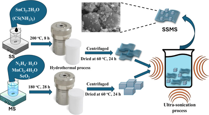
In a hydrothermal experiment, nanocrystalline SnS powder was prepared. 1.12 g of tin precursor SnCl2·2H2O and 2.25 g of thiourea (CS(NH2)2) were dissolved in water at a stoichiometric ratio of 1 : 2. For two hours, the material was mixed using a magnetic stirrer. After mixing, the resultant mixture was put into a 50 ml autoclave (Teflon-lined), filling up to 80% of the vessel. The autoclave underwent heat treatment in a hot air oven, fixed at 200 °C for 8 h. After the heat treatment, the autoclave was let to naturally cool to ambient temperature. After centrifugation, the resultant precipitate was removed from the reaction vessel and repeatedly cleaned with water and ethanol. The collected sample was dried overnight at a temperature of 60 °C. The sample SnS is mentioned as SS in the manuscript.
2.2.2. Synthesis of MnSe
Every reactant was of analytical quality and was used without additional purification. In a standard hydrothermal synthesis procedure, 0.1 mol SeO2 and 0.1 mmol MnCl2·4H2O were initially dissolved in 36 ml of deionized water. Subsequently, 30 minutes were spent magnetically stirring the above solution; 5 ml of N2H4·H2O was added. Then, the solution was put inside a 50 ml autoclave (Teflon-lined), sealed, and heated to 180 °C for 28 h. To get the final MnSe sample, the resultant solution was centrifuged three times with DI water and ethanol and kept overnight at 60 °C. Sample MnSe is referred to as MS in the manuscript.
2.2.3. Preparation of the SnS/MnSe (SSMS) heterostructure
0.1 g of SnS nanosheet and 0.1 g of MnSe nanoparticles were combined in 20 ml of DI water in a 50 ml glass beaker to create the SnS/MnSe heterostructure. The mixer was then placed in an ultrasonicator for 30 minutes. The final product was then dried for a whole night at 60 °C in an air oven. The overall synthesis process is shown in Fig. 1.
Fig. 1. Synthesis steps of SS, MS, and SSMS heterostructure samples by the hydrothermal method.
2.3. Characterization techniques
Different techniques were used to analyze the optical, morphological, and structural characteristics of the SSMS heterostructure. XRD was conducted using a Bruker D8 Advance diffractometer, having incident beam Cu Kα radiation (λ = 1.541 Å). The instrument was operated at 30 kV with 40 mA current, covering the angle from 15° to 75°. With an excitation wavelength of 532 nm, LABRAM-HR was utilized to conduct Raman measurements. TEM (JEOL, TEM-2100 plus) and FESEM (JEOL, JSM-7601FPLUS) instruments were used to examine the synthesized sample's morphology. Energy-dispersive X-ray spectroscopy (EDX) measurement examined the synthesized material's elemental distribution. Al Kα X-rays (1486.6 eV) were used to acquire core-level XPS spectra (Axis Ultra, Kratos Analytical, UK) in a 2 × 10⁻⁹ torr vacuum. The UV-vis-NIR spectrophotometer (JASCO-660) was used to examine the optical characteristics. The powder form of the sample was used to take the reflectance data in the UV measurement. The prepared powder sample's reflectance data were taken from 200 nm to 1800 nm using the integrating sphere obtained by UV visible spectroscopy. The current was measured using a Keithley 2450 source measuring device with a step size of 0.03. The voltage range was from −10 to +10 V. An LCR analyzer (Model PSM 1735, N4L) was utilized to evaluate the sample's dielectric properties across a wide temperature range, including ambient temperature to 450 °C and frequency over 1000 Hz to 1 MHz. For this investigation, we prepared a pellet of approximately 1 mm in thickness and 10 mm in diameter. For the dielectric test, the pellet was stored inside the furnace after it had been sintered for three hours at 150 °C. The dielectric parameters, including modulus (M′ and M′′), AC conductivity (σAC), impedance (Z′ and Z′′), and dielectric constant (εr), are determined for this study.
3. Results and discussion
3.1. XRD and Raman analysis
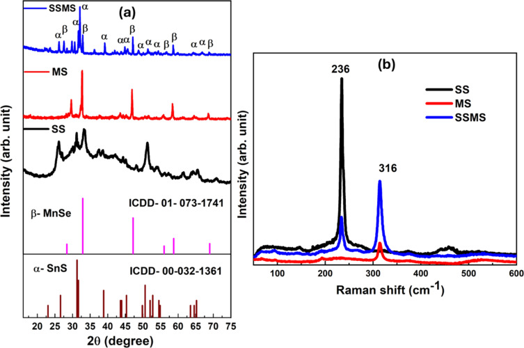
Since the work described in this research depends on understanding the crystal structures of SnS and MnSe, the in-depth structure analysis is done. The pyrite MnSe is an F3̄m space group member with a cubic crystal structure. Similarly, SnS is a Cmcm space group member with an orthorhombic crystal structure. The α-MnSe has a rock salt (NaCl) structure, which is stable at normal air pressure above room temperature. The second nearest neighbour, Mn atoms, is connected by Se atoms on its octahedral sites. By using X-ray diffraction analysis, the phase compositions of SnS and MnSe microcrystals were studied. As presented in Fig. 2(a), every diffraction peak can be positively identified as belonging to the cubic MnSe pyrite structure, having lattice constants of a = b = c = 5.4 Å (JCPDS No. 01-073-1741), and SnS orthorhombic crystal system with lattice constants of a = 4.17 Å, b = 11.42 Å, c = 4.12 Å with JCPDS No. 00-032-1361. The two pure phases were mixed to prepare the SnS and MnSe composite. The XRD pattern of MnSe shows peaks at 2θ angles of around 28.6, 32.7, 46.9, 55.8, 58.4, and 68.6 corresponding to the planes (1 1 1), (2 0 0), (2 2 0), (3 1 1), (2 2 2), and (4 0 0) respectively. Similarly, the observed peaks for the SnS phase are at 2θ angles of around 26.2, 31.3, 38.8, 43.9, 45.2, 48.9, 50.8, 54.3, 63.6, and 65.4, representing the planes as following (0 2 1), (0 4 0), (1 3 1), (0 0 2), (1 5 0), (1 1 2), (1 5 1), (2 4 0), (2 0 2), and (0 8 0) respectively. The XRD pattern shows no diffraction peaks due to any type of impurity. Every peak observed for the SSMS composite is attributed to both SnS and MnSe pristine phases. Thus, the observed diffraction patterns verify that the SnS/MnSe nanocomposite was successfully formed. Fig. S1† shows the Rietveld refinement of the SSMS sample done by X'pert Highscore Plus (PXHP) software. The scale factors and profile parameters are calibrated with respect to a standard profile. The reliability factors like the weighted profile factor (Rw.p.), expected factor (Rexp), and goodness-of-fit (χ2) were used to examine the quality of fit of the experimental data. The goodness-of-fit χ2 is defined as the ratio of Rw.p. and Rexp.25 The findings of different R factors of Rietveld refinement for the present sample, along with the lattice parameters, are as follows Rw.p. = 28.8, Rexp = 9.3, and the goodness-of-fit χ2 = 9.5. As we got the cubic phase of MnSe, the lattice parameters are a = 5.4 Å and orthorhombic for the SnS phase having a = 5.7 Å, b = 12.7 Å, c = 3.5 Å, respectively.
Fig. 2. (a) XRD patterns of SS, MS, and SSMS samples, and (b) Raman spectra of SS, MS, and SSMS samples.
The strain has a significant potential to affect the electronics and optical properties of the material. The change in strain can result in modifications to the bandgap and the electrical band structure. The strain due to lattice mismatch at the contact might modify the electrical band structure, either lowering or increasing the bandgap. Thus, material characteristics may be modified for specific uses through strain engineering.26 We have calculated the strain value of compositions from the XRD data and found that the SSMS composite has a lower strain value of 0.0025 than the pristine SS and MS compounds. At the same time, the SSMS has a lower bandgap value than the SS and MS, which might be due to the effect of tensile strain in the composite structure.27 The composite shows a low strain value as calculated from XRD data; therefore, strain has no significant effect on modulating the properties of the SSMS composite material.
The study of the structural alterations in the prepared samples was conducted using Raman spectroscopy. As shown in Fig. 2(b), spectroscopic analysis was conducted at room temperature from 50 to 600 cm−1. Vibrations associated with variations in polarizability and consequent modifications to the molecule structure can be more easily identified thanks to the Raman spectra. They contain details on atomic structures and chemical bonds. From the figure, it is observed that two notable peaks are present throughout the spectra. The sample SS has one peak at 316 cm−1, and sample MS has one prominent peak at 236 cm−1. The composite sample SSMS has both the peaks present in SS and MS samples in the same position. The peak at 316 cm−1 is assigned to the SnS vibrational band, which is absent in the MS sample and again reappeared in the SSMS composite sample.28 Likewise, the peak observed at 236 cm−1 for the MS sample is attributed to the longitudinal optical (LO) phonon mode of the MnSe system, which is absent in the SS ample and reappeared in the SSMS heterostructure sample.29 The observed data show good agreement with the XRD data. Raman analysis also confirms the formation of the SSMS heterostructure material.
3.2. FESEM, EDX, elemental mapping and TEM analysis
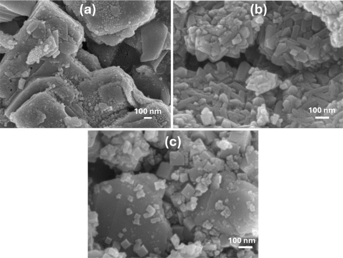
The morphology analysis was done using the FESEM images. Fig. 3 shows the morphology of SS, MS, and SSMS heterostructure samples. Here, we can observe that individual SS and MS samples show different shapes, and both shapes are found in the composite SSMS sample. It clearly shows the formation of the SSMS heterostructure. The SS sample shows nano sheet-like morphology having an average sheet length of 550 nm. Similarly, the MS sample has rectangular shapes with an average 120 nm length that are uniformly distributed throughout the sample. In the SSMS sample, the rectangular shapes of MS changed to cubic shapes. The SSMS sample has both the sheet and cubic shape morphology, confirming SSMS heterostructure formation.
Fig. 3. FESEM pictures of the (a) SS sample, (b) MS sample, and (c) SSMS heterostructure sample.
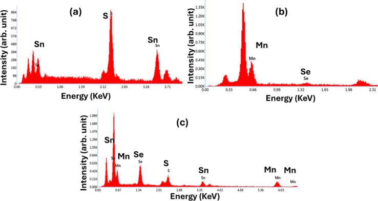
Fig. 4 shows the EDX images of all the prepared samples, confirming the corresponding compositional elements in the respective compositions. The SSMS heterostructure shows the presence of all the compositional elements, including Mn, Sn, S, and Se. The EDX table is presented in the ESI file.† Table S1† shows the atomic percentage of the compositional elements. The corresponding mapping image of the SSMS sample is presented in Fig. S2 of the ESI.†
Fig. 4. EDX images of the (a) SS sample, (b) MS sample, and (c) SSMS heterostructure.
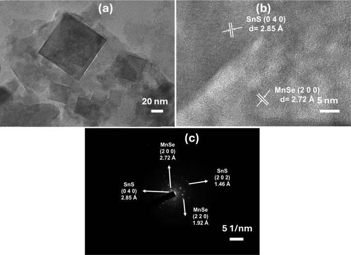
Additionally, the HR-TEM and SAED studies were used to calculate the particle size and crystallinity of the synthesized sample. Both nanosheets and cubic morphology are visible in the TEM picture of the SSMS heterostructure, as shown in Fig. 5(a). The value of lattice spacing is evaluated from the HRTEM images, and its associated lattice plane is depicted in Fig. 5(b). The spacing value is determined to be around 0.28 nm and 0.27 nm, which represents the (0 4 0) and (2 0 0) lattice planes of SnS and MnSe phases, respectively. Thus, it confirms the formation of the heterostructure, which also matches the XRD data of the SSMS sample. The SAED patterns represent the crystallinity of the sample shown in Fig. 5(c). The development of crystalline nanoparticles is confirmed by the SAED pattern, which looks into the particular ring pattern with bright spots. Overall, the structural analysis, including XRD, HRTEM, and SAED, shows that all the results are consistent and agree with each other.
Fig. 5. (a) TEM image, (b) HRTEM image, and (c) SAED pattern of the SSMS heterostructure.
3.3. Optical analysis
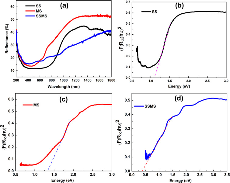
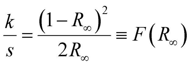
Fig. 6(a) illustrates the variation in reflectance with wavelength, which ranges from 200 to 1800 nm of prepared materials. UV-visible spectroscopy was used to get the synthesized material's reflectance data using an integrating sphere. It is noticed that the MS sample has a higher reflectance value than the SS sample, and the heterostructure shows the reflectance value between the MS and SS samples. In our earlier investigations, we found similar outcomes where SnMnSe has a higher reflectance value than SnMnS.30,31 The Kubelka–Munk principle was employed to calculate the optical band gap value from reflectance data.32 Suppose the particle size is the same or smaller with respect to the input light's wavelength, and the diffused reflectance spectra do not allow the secondary contributions of diffraction, refraction, and reflection. In that case, the reflectance is unaffected when the sample's thickness falls within the appropriate restriction. In the Kubelka–Munk theory ‘R∞’ represents the reflectance of an infinitely thick specimen.32 In that case, the Kubelka–Munk hypothesis is valid. This equation can be written as33
 |
1 |
R∞ is called the diffuse reflectance, and F(R) is considered the Kubelka–Munk function. Again, the optical band gap values Eg and the Tauc relation associate the absorption coefficient. The relation can be expressed as,34
| αhν = A(hν − Eg)m | 2 |
Fig. 6. (a) Reflectance of SS, MS, and SSMS samples, (b) direct bandgap of SS, (c) direct bandgap of MS, and (d) direct bandgap of the SSMS sample.
α is the linear absorption coefficient, A is the proportionality constant, and n is the frequency of light. For the crystalline samples, the value of “m” is taken as ½ to calculate the direct band gap. When the incoming light has exact diffuse scattering, then absorption k equals to 2α. In this case, the scattering coefficient ‘s’ is considered constant. Therefore, the absorption coefficient “k” and the F(R) are proportionate. By using eqn (2), we can get the expression.
| [F(R∞)hν]2 = A(hν − Eg) | 3 |
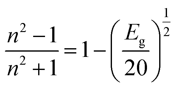
By drawing the (F(R∞)hν)2vs. hν, we can evaluate the bandgap of the synthesized material. Fig. 6(b–d) show the direct optical bandgap calculation, and the indirect bandgap calculations are presented in Fig. S3 of the ESI file.† The bandgap values of all the prepared samples are tabulated in Table 1. It was noticed that the bandgap of the synthesized materials had very small values.35 Similar results were found in our previous study. The MS has a bandgap value of 1.33 eV; similar results were also reported for the direct bandgap of the MnSe composition.36 The SM sample has an indirect bandgap value of around 0.86 eV, which matches the values reported previously.28 Qasem et al. have reported a bandgap value of around 1.22 eV for MnSe, which is nearly equal to the value we got in Table 1 for the MS sample.37 Similarly, SnS also has reported bandgap values from 1 to 1.2 eV, which is nearly equal to the calculated value we presented in Table 1.38 The prepared SSMS composite sample exhibits a low bandgap value. Several reports also suggest that the bandgap of the composite sample is lower than the pure composition due to the increase in the particle size.39,40 A common optical parameter crucial for applying optical materials in the construction of optoelectronic devices is the refractive index. Higher refractive index and lower bandgap materials are thought to be more effective options for use in solar cells, waveguides, and detectors.41 The ‘n’ value of the prepared material can be calculated by using the bandgap value in the Dimitrov and Sakka equation.42
 |
4 |
Optical parameters of SS, MS, and SSMS samples.
| Estimated optical parameters | SS | MS | SSMS |
|---|---|---|---|
| Direct optical bandgap (Eg) (eV) | 1.08 | 1.33 | 0.42 |
| Indirect optical bandgap (Eg) (eV) | 0.86 | 0.97 | 0.32 |
| Refractive index (n) | 3.30 | 3.10 | 4.32 |
| Dielectric constant (ε) | 10.90 | 9.63 | 18.70 |
The calculated refractive index varied according to the bandgap values. The dielectric constant is an important parameter that can indicate the capability of a material to concentrate the electric flux. It can be expressed as the ratio of sample's permittivity to the permittivity of free space (ε = n2). The obtained dielectric constant and refractive index values are shown in Table 1.
3.4. XPS analysis
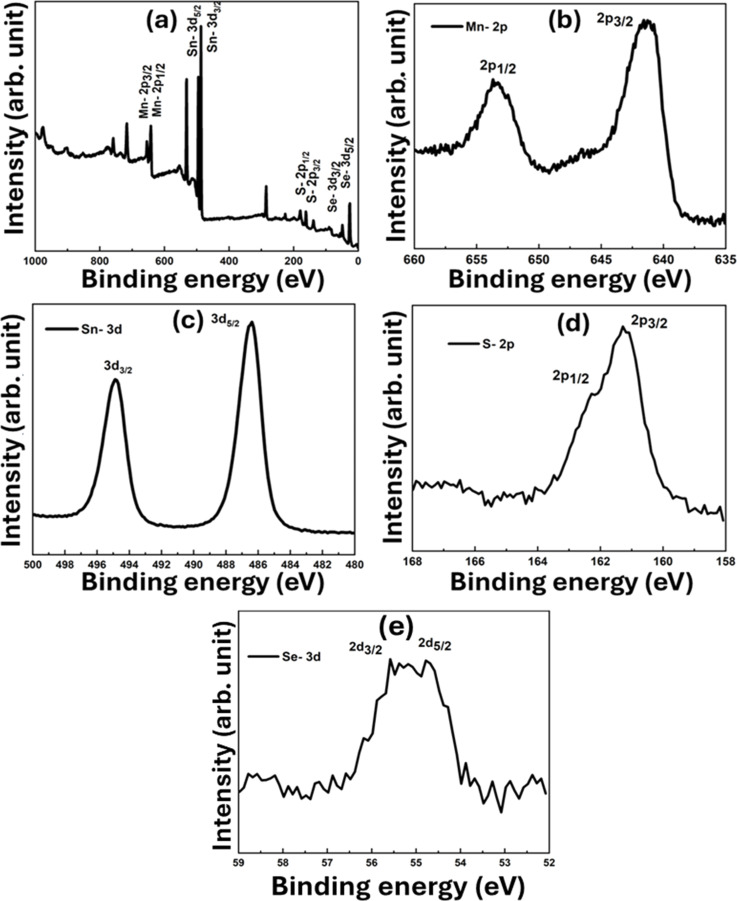
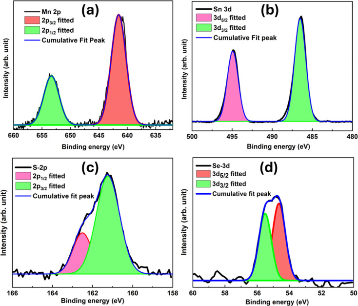
The XPS analysis aimed to investigate the elemental oxidation states in the produced sample. Surface science methods such as XPS are used to figure out the binding states and elements composed of materials. Since it can detect a wide variety of elements and their valence states, it is useful for identifying changes in a molecule's structure and their interactions with metal centers. Fig. 7(a) shows the survey scan of the SSMS sample, which confirms the presence of the constituent elements, namely Mn-2P, Sn-3d, S-2p, and Se-3d. The SSMS materials depicted in Fig. 7(b and e), which stand for Mn 2p and Se 3d, respectively, were subjected to XPS analysis to determine their chemical compositions and surface electronic states. Li et al. have reported that Mn2+ 2p1/2 and Mn2+ 2p3/2 are represented by peaks at 654.0 eV and 641.8 eV, respectively, and they denote the positive bivalent charge of the Mn ion.13 In the meanwhile, binding energies of 56.1 eV and 55.3 eV may be repeatedly ascribed to Se2− 3d3/2 and Se2− 3d5/2, respectively, indicating that the Se ion has minus two charges in the produced sample and is compatible with the mentioned study.43Fig. 7(c and d) show the XPS spectra of Sn-3d and S-2p elements. The figure shows that the peaks with the binding energies 494.8 and 486.3 eV are attributed to the Sn 3d3/2 and Sn 3d5/2, respectively.44 Similarly, the peaks at the binding energies 161 and 161.9 eV correspond to S 2p3/2 and S 2p1/2 respectively.45 These results provide evidence for the successful synthesis of the SSMS heterostructure. The fitting of XPS curves for all the compositional elements is presented in Fig. 8. From Fig. 8(a), we found that the deconvoluted peaks show clear peaks for Mn 2p½ and Mn 2p3/2 at 384 eV and 354 eV, respectively, having a peak separation energy of 11.8 eV. Menezes et al. have reported that the deconvoluted Mn 2p peaks show a spin–orbit level energy spacing of 11.5 eV and are typical for Mn3+-based materials.46 For element Sn, the peak separation energy is about 8.5 eV which is nearly equal to the separation energy of 8.6 eV as reported by Xia et al. for Sn4+.47 For element S, the fitting is proper with the peaks 2p1/2 and 2p3/2 at 161.9 and 161 eV, respectively. From Fig. 8(d), Se 3d5/2 peaked at 54.8 eV, and Se 3d3/2 peaked at 55.9 eV having a peak separation energy of 1.1 eV. In the present study, the binding energies of Se 3d5/2 and Se 3d3/2 were between 54.6 and 57.5 eV, indicating that the particulate matter was elemental Se. The report by Han et al. states that the Se 3d peak binding energy of Se(iv) was greater than 58.0 eV, with elemental Se ranging from 54.6 to 57.5 eV and Se compounds ranging from 52.8 to 55.7 eV.48
Fig. 7. XPS spectra of (a) SSMS survey, (b) Mn 2p, (c) Sn 3d, (d) S 2p, and (e) Se 3d.
Fig. 8. XPS peak fitting of compositional elements (a) Mn 2p, (b) Sn 3d, (c) S 2p, and (d) Se 3d.
3.5. Electrical analysis
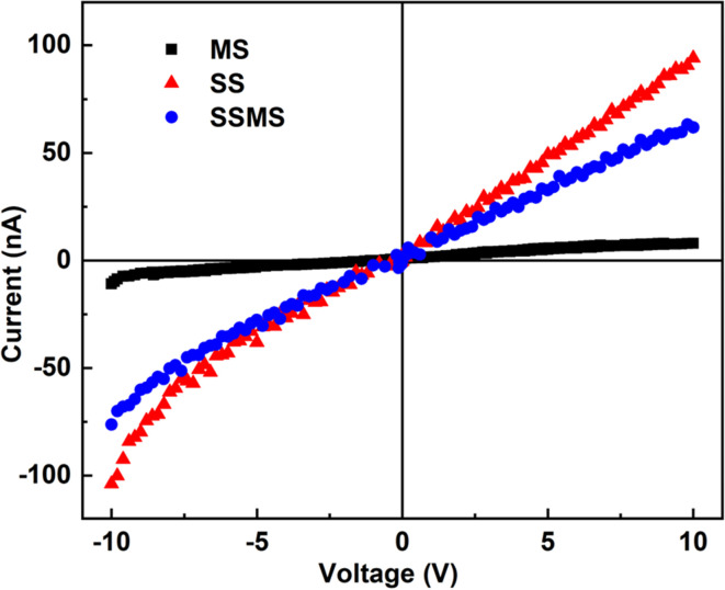
Studies have been done on the material's electrical characteristics in light of its possible application in the manufacturing of optoelectronic devices. At ambient temperature, the I–V experiment was done with a DC voltage scanned from −10 to +10 V. The I–V curve for synthesized samples is displayed in Fig. 9. The MS sample shows good electrical characteristics, whereas the SS sample shows relatively low electrical characteristics. The SSMS sample shows different electrical properties from both the SS and MS samples, and the values lie between the two pure phases. Thus, it also confirms the formation of the SSMS heterostructure of two pure phases SS and MS. The SS sample shows a maximum current of 97 nA, whereas the MS sample shows a maximum current value of 8.5 nA, and the heterostructure SSMS shows a maximum current of 64 nA under light conditions. The comparative I–V plots of all the samples under both dark and light conditions are shown in Fig. S4 of the ESI file† for a comparative study. Here, it can be observed that the light current shows a higher value than the dark current in all three cases.49 This increase in photocurrent compared to the dark current can be attributed to the charge separation and the interaction between the light and material.
Fig. 9. I–V characteristics of SS, MS, and SSMS samples.
3.6. Dielectric study
3.6.1. Dielectric constant, AC conductivities, and dielectric loss
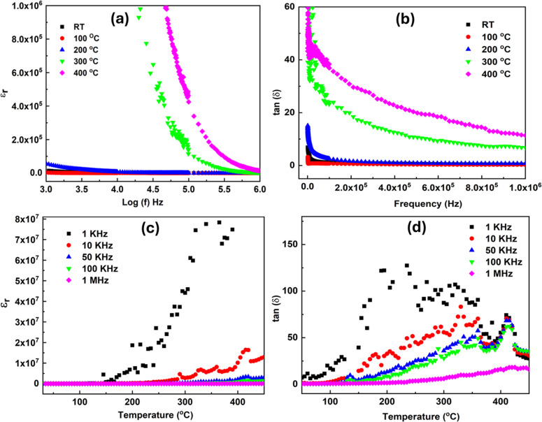
The dielectric characterization explains the electrical characteristics of the prepared nanoparticles and their impact on grain boundaries. Contributions from dipolar, ionic, and space charge elements can all affect the sample's dielectric characteristics. The modification of dielectric parameters of polycrystalline samples in the optical frequency range is greatly influenced by electronic polarizability. The separation of positive and negative ions causes ionic polarization.50 Surface roughness is one morphological characteristic that might alter the dielectric properties by changing the surface states and trapping processes. Rough surfaces can disperse charge carriers, altering both conductivity and dielectric loss.11 The material's capacity to polarize in reaction to an external electric field affects its dielectric characteristics. Chemical states, grain boundaries, and crystal structure are important factors. Minimal dielectric loss is essential for effective energy storage and transfer, and high dielectric constant materials are preferred for capacitors. Temperature and frequency dependence of the sample dielectric properties are investigated. Fig. 10(a) and (b) show the dielectric constant and loss tangent variation based on the sample SSMS frequency. Both εr and the loss tangent exhibit a reduction of values that becomes steady at higher frequencies as the frequency increases. Coskun et al. have also observed that the real dielectric constant declines as the frequency increases.51 The phenomenological theory of Maxwell–Wagner and Koop shows different polarization processes that can explain the dielectric characteristics. The observed high values of εr and dielectric loss at the low-frequency range may be due to the influence of different factors like the electron cloud's displacement, the dipole's orientation along the field direction, the development of space charges, and the ion separation over short distances.52,53 The overall polarization is reduced since the electron follows the rapidly varying frequency. Therefore, at high frequencies, both loss of tangent value and a decrease in the dielectric constant are caused by the decline in the polarization value.
Fig. 10. (a) The frequency-dependent dielectric constant, and (b) dielectric loss. (c) The temperature-dependent dielectric constant, and (d) loss tangent of SSMS.
The εr and tan (δ) fluctuations, according to the temperature of the sample SSMS, are displayed in Fig. 10(c) and (d). Temperature, ionic, and dipolar polarization are the main factors influencing low-frequency fluctuations in the dipole and ions. As a result, the amount of εr and dielectric loss grow in increasing order as temperature rises. Furthermore, there is a large dissipation factor in the composite, including magnetic components.54,55 The dielectric constant results show that as temperature rises, peak intensity diminishes at higher frequencies. The material's dielectric relaxation phenomenon may be the cause of this behavior.56
The changes of AC conductivities according to frequency and temperature are depicted in Fig. S5(a) and (b).† These values are calculated through the equation σAC = ω tan δεrεo, here ω is the angular frequency, εo is the permeability of free space. At low frequencies, the material's AC conductivities become noticeably more apparent. The onset of AC conductivity is referred to as the hopping frequency. The hopping frequency rises as the temperature rises, suggesting that conductivity is temperature-dependent and possibly thermally regulated. As a function of frequency, conductivity values are higher at low regions, which might be because of grain boundary contribution. Similar outcomes were also obtained in our earlier work. Similarly, the change in conductivities with respect to inverse temperature at different frequencies is shown in Fig. S5(b).† An increase in temperature excites the charge carriers over a small distance, leading to improved conductivities.
3.6.2. Impedance and modulus spectrum analysis
Complex impedance spectroscopy (CIS) serves as a method for investigating the electrical attributes and diverse relaxation activities within dielectric materials.57,58 In the necessary frequency domain, both parts, real and imaginary of complex impedance are evaluated at once and can be shown as,59
| Z = Z′ − iZ′′ | 5 |
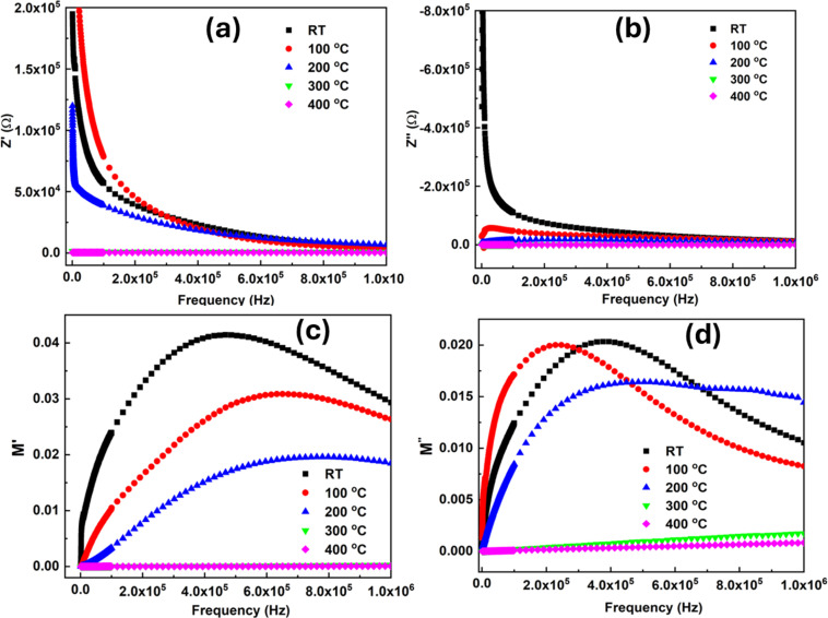
where Z′ = Z cos θ and Z′′ = Z sin θ are real and imaginary parts of impedance, respectively. The measurement of Z′ and Z′′ according to frequency is depicted in Fig. 11(a) and (b). It is evident from the graph that when the temperature and frequency rise, the Z′ value falls. At high frequencies, the dissipation of space charges at grain boundaries is depicted by the convergence of Z′ curves at temperatures exceeding 1000 kHz. This convergence also signifies the constancy of conductivity at elevated frequencies. The curve for Z′ with frequency at various temperatures monotonically decreases with a negative slope. This result of Z′ indicates that the SSMS sample has semiconducting characteristics.60 The behavior of Z′, which exhibits a decrease with rising temperature and frequency, is consistent with the increasing conductivity with increasing temperature and frequency. This behavior demonstrated a link between the sample's conducting and resistivity characteristics.61 The Z′ exhibits a constant value at high frequencies at various temperatures, which indicates the space charge release. The resistive qualities become less as temperature increases, leading to an increase in AC conductivity as the material temperature rises. Fig. S6 in the ESI file† displays the Nyquist plot of the SSMS sample for 100 °C and at room temperature data. The inset figures display the corresponding circuit arrangement (Q(RQ)). The different patterns show the electrical processes that are going on within the sample and may be connected to the microstructure changes that had an impact on the dielectric and electrical conductivity.
Fig. 11. (a) Plot of (Z′) versus frequency, (b) Z′′ versus frequency, and (c and d) temperature-dependent alteration in the M′ and M′′ with frequency.
Fig. 11(b) depicts the imaginary component Z′′ fluctuation with the frequency. It is evident from the figure that when the frequency rises, the Z′′ decreases. The steady decline in Z′′ indicates that there is less current dissipation in lower temperature zones. Z′′ descends toward higher frequencies before merging at all temperatures, indicating that space charge has accumulated in the sample. It has been demonstrated that complex impedance analysis can identify the transport characteristics that occur between the grain and grain boundaries and provide a more thorough explanation for the variations in conductivity (both ac and dc), dielectric losses, and dielectric permittivity.
The investigation in electric modulus M* gives a basic knowledge of the electrode polarization effect, conductivity mechanisms, and relaxation processes that take place in the generated sample.62,63 The electric modulus M* is composed of two components: the real part (M′) and the imaginary part (M′′). The real component can be represented as M′ = (−1)ωCoZ′′, while the imaginary component is given by M′′ = ωCoZ′. Here, ω denotes the angular frequency, and Co = εoA/d represents the geometrical capacitance of the dielectric material.63 where
where 
The M′ approaches zero for higher temperature conditions at lower frequency ranges, as shown in Fig. 11(c), indicating a negligible electrode effect. The relaxation peak on the low-frequency side of the frequency versus M′′ curves approaches the high-frequency side as the temperature rises. This shows the dielectric relaxation in the prepared sample that is regulated by heat, indicative of non-Debye-type behavior.64
4. Conclusion
In this work, we synthesized SnS and MnSe compositions using the hydrothermal method and then prepared the SnS/MnSe heterostructure. We investigated the structural, optical, electrical, and dielectric properties of the SnS/MnSe heterostructure. The structural analysis confirms the formation of the SnS/MnSe heterostructure from the SnS and MnSe pure phases. The individual MnSe and SnS compositions exhibit suitable optical characteristics with bandgap values of around 1.3 and 1 eV, respectively, while the prepared SnS/MnSe heterostructure has a very low bandgap value of about 0.4 eV. As a result of low bandgap values, the sample shows a high refractive index, which was calculated utilizing the Dimitrov and Sakka formula. Both pure phases showed different morphologies, but both morphological shapes were detected in the SnS/MnSe heterostructure. The SnS/MnSe sample shows different electrical properties from both the SS and MS samples and the values lie between the two pure phases. The dielectric measurement showed the increment of εr and tan (δ) with the rise in temperature and frequency decline. This is because of the macroscopic distortion of charges and space charge polarization. At low frequencies, the AC conductivities showed high values and increased for higher temperatures. The prepared SnS/MnSe heterostructure shows different optical and electrical properties than the pure phases. All the above results indicate that the SnS/MnSe heterostructure can be used in optoelectronics and dielectric applications.
Data availability
Data will be made available upon request from the corresponding author.
Conflicts of interest
The authors declare no competing financial interest.
Supplementary Material
Acknowledgments
The author, Dr R. Naik, acknowledges the central instrument facility of ICT-IOC for different characterization and the Science and Engineering Research Board, Govt. of India, for financial support (DST/CRG/2022/003084).
Electronic supplementary information (ESI) available: Rietveld refinement of XRD patterns; elemental mapping of corresponding elements of the SSMS heterostructure; indirect optical bandgap calculation of SS, MS, and SSMS samples; comparative plot of light and dark current of all the prepared samples; AC conductivity at different temperatures, frequency as a function of frequency and temperature; Nyquist plot of the SSMS sample for 100 °C and at room temperature; atomic percentage of constituent elements, respectively, of the SSMS heterostructure sample. See DOI: https://doi.org/10.1039/d4na00684d
References
- Reddy K. T. R. Reddy P. P. Datta P. K. Miles R. W. Thin Solid Films. 2002;403–404:116–119. doi: 10.1016/S0040-6090(01)01520-6. [DOI] [Google Scholar]
- Tanusevski A. Semicond. Sci. Technol. 2003;18:501. doi: 10.1088/0268-1242/18/6/318. [DOI] [Google Scholar]
- Burton L. A. Whittles T. J. Hesp D. Linhart W. M. Skelton J. M. Hou B. Webster R. F. O'Dowd G. Reece C. Cherns D. Fermin D. J. Veal T. D. Dhanak V. R. Walsh A. J. Mater. Chem. A. 2016;4:1312–1318. doi: 10.1039/C5TA08214E. [DOI] [Google Scholar]
- Ahn J. H. Lee M. J. Heo H. Sung J. H. Kim K. Hwang H. Jo M. H. Nano Lett. 2015;15:3703–3708. doi: 10.1021/acs.nanolett.5b00079. [DOI] [PubMed] [Google Scholar]
- Ichimura M. Takeuchi K. Ono Y. Arai E. Thin Solid Films. 2000;361–362:98–101. doi: 10.1016/S0040-6090(99)00798-1. [DOI] [Google Scholar]
- Deb A. K. Kumar V. Phys. Status Solidi. 2017;254:1600379. doi: 10.1002/pssb.201600379. [DOI] [Google Scholar]
- Zhu H. Yang D. Zhang H. Mater. Lett. 2006;60:2686–2689. doi: 10.1016/j.matlet.2006.01.065. [DOI] [Google Scholar]
- Reddy N. K. Reddy K. T. R. Mater. Chem. Phys. 2007;102:13–18. doi: 10.1016/j.matchemphys.2006.10.009. [DOI] [Google Scholar]
- Banai R. E. Horn M. W. Brownson J. R. S. Sol. Energy Mater. Sol. Cells. 2016;150:112–129. doi: 10.1016/j.solmat.2015.12.001. [DOI] [Google Scholar]
- Andrade-Arvizu J. A. Courel-Piedrahita M. Vigil-Galan O. J. Mater. Sci. Mater. Electron. 2015;26:4541–4556. doi: 10.1007/s10854-015-3050-z. [DOI] [Google Scholar]
- Yang Y. Zhou Y. Luo Z. Guo Y. Rao D. Yan X. Phys. Chem. Chem. Phys. 2019;21:9296–9301. doi: 10.1039/C9CP00427K. [DOI] [PubMed] [Google Scholar]
- Mao Y. Xu C. Yuan J. A Zhao H. J. Mater. Chem. A. 2019;7:11265–11271. doi: 10.1039/C9TA01219B. [DOI] [Google Scholar]
- Li N. Zhang Y. Zhao H. Liu Z. Zhang X. Du Y. Inorg. Chem. 2016;55:2765–2770. doi: 10.1021/acs.inorgchem.5b02558. [DOI] [PubMed] [Google Scholar]
- Sines I. T. Misra R. Schiffer P. Schaak R. E. Angew. Chem. Int. 2010;49:4638–4640. doi: 10.1002/anie.201001213. [DOI] [PubMed] [Google Scholar]
- Angadi M. A. Thanigaimani V. Phys. Status Solidi. 1993;135:183–190. doi: 10.1002/pssa.2211350114. [DOI] [Google Scholar]
- Chen H. Guo Y. Ma P. Hu R. Khatoon R. Lu Y. Zhu H. Lu J. J. Electroanal. Chem. 2019;847:113205. doi: 10.1016/j.jelechem.2019.113205. [DOI] [Google Scholar]
- Cheng K. W. Wu Y. H. Chiu T. H. J. Power Sources. 2016;307:329–339. doi: 10.1016/j.jpowsour.2015.12.090. [DOI] [Google Scholar]
- Tang C. Li Q. Zhang C. He C. Li J. Ouyang T. Li H. Zhong J. J. Phys. D Appl. Phys. 2018;51:245004. doi: 10.1088/1361-6463/aac3eb. [DOI] [Google Scholar]
- Masrat S. Poolla R. Dipak P. Zaman M. B. Surface. Interfac. 2021;23:100973. doi: 10.1016/j.surfin.2021.100973. [DOI] [Google Scholar]
- Nerella M. Suresh M. B. Bathulapalli S. Phys. B Condens. Matter. 2022;627:413534. doi: 10.1016/j.physb.2021.413534. [DOI] [Google Scholar]
- Musahwar N. Majeed Khan M. A. Husain M. Zulfequar M. J. Phys. D Appl. Phys. 2007;40:7787. doi: 10.1088/0022-3727/40/24/029. [DOI] [Google Scholar]
- Gao M. R. Xu Y. F. Jiang J. Yu S. H. Chem. Soc. Rev. 2013;42:2986–3017. doi: 10.1039/C2CS35310E. [DOI] [PubMed] [Google Scholar]
- Das S. Senapati S. Naik R. J. Alloys Compd. 2023;968:171923. doi: 10.1016/j.jallcom.2023.171923. [DOI] [Google Scholar]
- Hussain R. A. Hussain I. Mater. Chem. Phys. 2020;256:123691. doi: 10.1016/j.matchemphys.2020.123691. [DOI] [Google Scholar]
- Parida A. Senapati S. Pradhan G. K. Naik R. ChemistrySelect. 2023;8:e202301933. doi: 10.1002/slct.202301933. [DOI] [Google Scholar]
- Cao X. Xu P. Zhang X. Huan H. Zhou L. Zhang C. Tribol. Lett. 2024;72:1–11. doi: 10.1007/s11249-023-01800-w. [DOI] [Google Scholar]
- Wei B. Zheng K. Ji Y. Zhang Y. Zhang Z. Han X. Nano Lett. 2012;12:4595–4599. doi: 10.1021/nl301897q. [DOI] [PubMed] [Google Scholar]
- Buckley J. J. McCarthy C. L. Del Pilar-Albaladejo J. Rasul G. Brutchey R. L. Inorg. Chem. 2016;55:3175–3180. doi: 10.1021/acs.inorgchem.6b00243. [DOI] [PubMed] [Google Scholar]
- Popovic Z. V. Milutinovic A. Phys. Rev. B: Condens. Matter Mater. Phys. 2006;73:155203. doi: 10.1103/PhysRevB.73.155203. [DOI] [Google Scholar]
- Parida A. Senapati S. Pradhan G. K. Naik R. J. Alloys Compd. 2024;970:172520. doi: 10.1016/j.jallcom.2023.172520. [DOI] [Google Scholar]
- Parida A. Senapati S. Samal S. Bisoyi S. Naik R. ACS Appl. Nano Mater. 2023;6:11230–11241. doi: 10.1021/acsanm.3c01260. [DOI] [Google Scholar]
- Makuła P. Pacia M. Macyk W. J. Phys. Chem. Lett. 2018;9:6814–6817. doi: 10.1021/acs.jpclett.8b02892. [DOI] [PubMed] [Google Scholar]
- Landi S. Segundo I. R. Freitas E. Vasilevskiy M. Carneiro J. Tavares C. J. Solid State Commun. 2022;341:114573. doi: 10.1016/j.ssc.2021.114573. [DOI] [Google Scholar]
- Tauc J., Amorph. Liq. Semicond. 1974, pp. 159–220 [Google Scholar]
- Sheng C. Bu Y. Li Y. Su L. Yu Y. Cao D. Zhou J. Chen X. Lu W. Shu H. ACS Appl. Mater. Interfaces. 2022;15:14704–14714. doi: 10.1021/acsami.2c21958. [DOI] [PubMed] [Google Scholar]
- Jevtovic V. Khan A. U. Almarhoon Z. M. Tahir K. Latif S. Abdulaziz F. Albalawi K. Zaki M. E. A. Rakic V. Nanomater. 2023;13:667. doi: 10.3390/nano13040667. [DOI] [PMC free article] [PubMed] [Google Scholar]
- Qasem A. Said N. M. Hassan A. A. Yakout H. A. Shaaban E. R. Physica B: Condensed Matter. 2022;627:413600. doi: 10.1016/j.physb.2021.413600. [DOI] [Google Scholar]
- Iqbal M. Z. Wang F. Rafique M. Y. Ali S. Farooq M. H. Ellahi M. Mater. Lett. 2013;106:33–36. doi: 10.1016/j.matlet.2013.04.051. [DOI] [Google Scholar]
- Sajana J. V. S. Perera D. Mater. Sci. 2023:10946. [Google Scholar]
- Sitt A. Hadar I. Banin U. Nano Today. 2013;8:494–513. doi: 10.1016/j.nantod.2013.08.002. [DOI] [Google Scholar]
- Yakuphanoglu F. Cukurovali A. Yilmaz I. Opt. Mater. 2005;27:1363–1368. doi: 10.1016/j.optmat.2004.09.021. [DOI] [Google Scholar]
- Dimitrov V. Sakka S. J. Appl. Phys. 1996;79:1736–1740. doi: 10.1063/1.360962. [DOI] [Google Scholar]
- Yang J. Yuan Y. Wang W. Tang H. Ye Z. Lu J. J. Power Sources. 2017;340:6–13. doi: 10.1016/j.jpowsour.2016.11.061. [DOI] [Google Scholar]
- Kafashan H. Azizieh M. Nasiri Vatan H. J. Alloys Compd. 2016;686:962–968. doi: 10.1016/j.jallcom.2016.06.201. [DOI] [Google Scholar]
- Wang W. Shi L. Lan D. Li Q. J. Power Sources. 2018;377:1–6. doi: 10.1016/j.jpowsour.2017.11.084. [DOI] [Google Scholar]
- Menezes P. W. Indra A. Gutkin V. Driess M. Chem. Commun. 2017;53:8018–8021. doi: 10.1039/C7CC03749J. [DOI] [PubMed] [Google Scholar]
- Xia W. Wang H. Zeng X. Han J. Zhu J. Zhou M. Wu S. CrystEngComm. 2014;16:6841–6847. doi: 10.1039/C4CE00884G. [DOI] [Google Scholar]
- Han D. S. Batchelor B. Abdel-Wahab A. Environ. Prog. Sustain. Energy. 2013;32:84–93. doi: 10.1002/ep.10609. [DOI] [Google Scholar]
- Kumar P. C. Mohapatra A. Senapati S. Pradhan M. Naik R. FlatChem. 2023;42:100580. doi: 10.1016/j.flatc.2023.100580. [DOI] [Google Scholar]
- Suresh S. Int. J. Phys. Sci. 2014;9:380–385. [Google Scholar]
- Coskun R. Yalçın O. Okutan M. Mater. Chem. Phys. 2023;296:127171. doi: 10.1016/j.matchemphys.2022.127171. [DOI] [Google Scholar]
- Sahoo D. Senapati S. Samal S. Varadharajaperumal S. Naik R. ACS Appl. Eng. Mater. 2023;1:1001–1012. doi: 10.1021/acsaenm.2c00269. [DOI] [Google Scholar]
- Mehedi Hassan M. Ahmed A. S. Chaman M. Khan W. Naqvi A. H. Azam A. Mater. Res. Bull. 2012;47:3952–3958. doi: 10.1016/j.materresbull.2012.08.015. [DOI] [Google Scholar]
- Shaikh A. M. Bellad S. S. Chougule B. K. J. Magn. Magn Mater. 1999;195:384–390. doi: 10.1016/S0304-8853(99)00138-9. [DOI] [Google Scholar]
- Mohanty N. K. Behera A. K. Satpathy S. K. Behera B. Nayak P. J. Rare Earths. 2015;33:639–646. doi: 10.1016/S1002-0721(14)60465-8. [DOI] [Google Scholar]
- Sahoo D. Senapati S. Samal S. Bisoyi S. Naik R. Mater. Today Electron. 2023;3:100030. doi: 10.1016/j.mtelec.2023.100030. [DOI] [Google Scholar]
- Brunig M. Gerke S. Schmidt M. MoS D. Zhang S. Wen Z. Patarroyo M. Vera E. Pineda Y. Gomez J. Soraca G. Sánchez D. J. Phys. Conf. 2017;786:012014. doi: 10.1088/1742-6596/786/1/012014. [DOI] [Google Scholar]
- Gupta G. K. Garg A. Dixit A. J. Appl. Phys. 2018;123:013101. doi: 10.1063/1.5002619. [DOI] [Google Scholar]
- Joshi J. H. Kanchan D. K. Joshi M. J. Jethva H. O. Parikh K. D. Mater. Res. Bull. 2017;93:63–73. doi: 10.1016/j.materresbull.2017.04.013. [DOI] [Google Scholar]
- Samal S. K. Biswal B. Mallick M. K. Choudhary R. N. P. Bhuyan S. J. Mater. Sci. 2022;57:9312–9322. doi: 10.1007/s10853-022-07254-0. [DOI] [Google Scholar]
- Wu J. Wang J. Xiao D. Zhu J. J. Appl. Phys. 2011;6:110. [Google Scholar]
- Ben Bechir M. Karoui K. Tabellout M. Guidara K. Ben Rhaiem A. Phase Transitions. 2018;91:901–917. doi: 10.1080/01411594.2014.987673. [DOI] [Google Scholar]
- Ohki Y. IEEJ Trans. Electr. Electron. Eng. 2022;17:958–972. doi: 10.1002/tee.23565. [DOI] [Google Scholar]
- Bag S. Das P. Behera B. J. Theor. Appl. Phys. 2017;11:13–25. doi: 10.1007/s40094-017-0246-z. [DOI] [Google Scholar]
Associated Data
This section collects any data citations, data availability statements, or supplementary materials included in this article.
Supplementary Materials
Data Availability Statement
Data will be made available upon request from the corresponding author.


