Abstract
AlGaN is attractive for fabricating deep ultraviolet (DUV) optoelectronic and electronic devices of light-emitting diodes (LEDs), photodetectors, high-electron-mobility field-effect transistors (HEMTs), etc. We investigated the quality and optical properties of AlxGa1−xN films with high Al fractions (60–87%) grown on sapphire substrates, including AlN nucleation and buffer layers, by metal–organic chemical vapor deposition (MOCVD). They were initially investigated by high-resolution X-ray diffraction (HR-XRD) and Raman scattering (RS). A set of formulas was deduced to precisely determine x(Al) from HR-XRD data. Screw dislocation densities in AlGaN and AlN layers were deduced. DUV (266 nm) excitation RS clearly exhibits AlGaN Raman features far superior to visible RS. The simulation on the AlGaN longitudinal optical (LO) phonon modes determined the carrier concentrations in the AlGaN layers. The spatial correlation model (SCM) analyses on E2(high) modes examined the AlGaN and AlN layer properties. These high-x(Al) AlxGa1−xN films possess large energy gaps Eg in the range of 5.0–5.6 eV and are excited by a DUV 213 nm (5.8 eV) laser for room temperature (RT) photoluminescence (PL) and temperature-dependent photoluminescence (TDPL) studies. The obtained RTPL bands were deconvoluted with two Gaussian bands, indicating cross-bandgap emission, phonon replicas, and variation with x(Al). TDPL spectra at 20–300 K of Al0.87Ga0.13N exhibit the T-dependences of the band-edge luminescence near 5.6 eV and the phonon replicas. According to the Arrhenius fitting diagram of the TDPL spectra, the activation energy (19.6 meV) associated with the luminescence process is acquired. In addition, the combined PL and time-resolved photoluminescence (TRPL) spectroscopic system with DUV 213 nm pulse excitation was applied to measure a typical AlGaN multiple-quantum well (MQW). The RT TRPL decay spectra were obtained at four wavelengths and fitted by two exponentials with fast and slow decay times of ~0.2 ns and 1–2 ns, respectively. Comprehensive studies on these Al-rich AlGaN epi-films and a typical AlGaN MQW are achieved with unique and significant results, which are useful to researchers in the field.
Keywords: AlGaN-GaN, high x(Al), metal–organic chemical vapor deposition, spectroscopic ellipsometry, X-ray diffraction, Raman scattering, photoluminescence, temperature-dependent and time-resolved photoluminescence
1. Introduction
Wide-bandgap nitride-based semiconductors, devices, and applications have been greatly developed in recent decades [1,2,3]. Ultra-wide-gap (UWG) semiconductors (Eg > 5 eV), including AlN, diamond, β-Ga2O3, and AlGaN with high Al compositions, possess excellent material properties for promoting the development of the next generation of power electronics. AlxGa1−xN materials cover the energy range between 3.4 eV (x = 0) and 6.2 eV (x = 1) and high-x (x > 50%). AlxGa1−xN is very attractive in deep ultraviolet (DUV) devices and applications. In the past two decades, intense research and development (R&D) emerged on high-x AlxGa1−xN epi-materials [4,5,6,7,8,9,10,11,12,13,14], Al-rich AlGaN multiple-quantum wells (MQWs) [15,16], AlGaN DUV light-emitting diodes (LEDs) [17,18], AlGaN DUV laser diodes (LDs) [19], high-x(Al) AlGaN field-effect transistors (FETs) [20,21], Al-rich high-electron-mobility transistors (HEMTs) [22,23,24,25], and so on. R&D on Al-rich AlGaN materials and devices are the current frontiers and hot points in the field [9,10,11,12,13,14,16,17,18,19,22,23,24,25].
In the current work, we investigated the optical and structural properties of AlxGa1−xN films with high x(Al) (60%, 71%, 75%, 81%, 87%) fractions grown on C-plane sapphire substrates with a 20 nm AlN nucleation layer and an AlN buffer layer by metal–organic chemical vapor deposition (MOCVD). To characterize these AlGaN/AlN/sapphire structures well via high-resolution X-ray diffraction (HR-XRD), we deduced a set of formulas to precisely determine the x(Al) from three orders of HR-XRD data. Screw dislocation densities in AlGaN and AlN layers were deduced. The AlGaN/AlN/sapphire structures were also characterized by visible and DUV Raman scattering (RS). The DUV (266 nm) excitation RS clearly exhibited AlGaN Raman features far superior to visible RS. Two types of simulation methods were applied to analyze the Raman longitudinal optical (LO) and E2(high) phonon modes. The carrier concentrations in the AlGaN layers were determined via simulation on the AlGaN longitudinal optical (LO) phonon modes. The Raman line shapes of E2(high) modes were analyzed by the spatial correlation model (SCM), which qualitatively investigated the AlGaN and AlN layer properties. Room temperature (RT) photoluminescence (PL) and temperature-dependent photoluminescence (TDPL) measurements were carried under the excitation from a DUV 213 nm (5.8 eV) laser to investigate these high-x(Al) AlxGa1−xN films with energy gaps Eg between 5.0 and 5.6 eV. The obtained PL bands were deconvoluted with Gaussian bands, indicating cross-bandgap emission, phonon replicas, and variation with x(Al). TDPL spectra at 20–300 K of Al0.87Ga0.13N exhibit the T-dependences of the band-edge luminescence near 5.6 eV and the phonon replicas. According to the Arrhenius fitting diagram of the TDPL spectra, the activation energy (19.6 meV) associated with the luminescent process is acquired. In addition, a combined PL and time-resolved photoluminescence (TRPL) spectroscopic system with DUV 213 nm pulse excitation was applied to investigate AlGaN multiple-quantum wells (MQWs). RT TRPL decay spectra were measured at four wavelengths and fitted by two exponentials, with fast and slow decay times obtained. Comprehensive findings on the material qualities and optical properties of Al-rich AlGaN epi-films and a typical AlGaN MQW are achieved with attractive results, which provide useful references to the R&D in AlGaN and related materials.
2. Materials and Methods
For the material growth procedure on the C-plane sapphire substrate by metal–organic chemical vapor deposition (MOCVD), a low-temperature (LT)-AlN nucleation layer of 20 nm was first grown at 600 °C. Then, an HT-AlN buffer layer was grown at an increased temperature of 1050 °C; subsequently, AlxGa1−xN layers with different x(Al) compositions were grown at the same temperature of 1050 °C. Precursors of trimethyl-aluminum (TMAl), trimethyl-gallium (TMGa), and ammonia (NH3) were used for Al, Ga, and N, respectively. The growth details are like those reported in [26]. The experimental samples are named A60, A71, A75, A81, and A87, with x(Al) in AlxGa1−xN of 60.2%, 71.4%, 75.3%, 81.1%, and 87.7% determined in this study, respectively. An additional sample A35 with lower x(Al) of 35.0% is used for reference as performing XRD measurements. The AlGaN layer thicknesses are in the range of 400–600 nm, determined from spectroscopic ellipsometry (SE) measurements, like those reported in [27].
In the present work, high-resolution X-ray diffraction (HR-XRD) measurements were conducted from a system of Bruker D8 Discover, Ettlingen, Germany. SE measurements were carried out by using a Mueller matrix ellipsometer, model ME-L, from Wuhan Eoptics Technology Co. Ltd., Wuhan, China, with five or three incident angles of 50–70°. DUV 266 nm excitation Raman scattering measurements were performed at room temperature (RT), by using a confocal microscope optical system, including two lasers of 266 nm and 532 nm, and a spectrometer of iHR550 (Horiba, Irvine CA, USA) with gratings of 600 g/mm and 2400 g/mm. A combined photoluminescence (PL) and time-resolved photoluminescence (TRPL) spectroscopic system with deep ultraviolet (DUV) 213 nm excitation was built up and applied to measure AlGaN multiple quantum wells (MQWs) and high Al-composition AlGaN epi-films as well as other ultrawide bandgap (UBG) materials and structures. In DUV 213 nm excitation steady-state photoluminescence (SS-PL), temperature-dependent (TD) PL, and time-resolved PL (TRPL) experiments, samples were excited by a CNI FL-213-Pico 213 nm picosecond laser. The PL decay curves were recorded by a time-correlated single-photon-counting (TCSPC) system, as in [28]. DUV 193 nm excitation PL measurements were also conducted with a 193 nm laser source, and UV–visible optical transition measurements were carried out using a UV–visible spectrophotometer (Zolix OmniAs, Beijing, China) with deuterium lamps, as described in [29].
3. Results and Discussions
3.1. High-Resolution X-Ray Diffraction Analysis
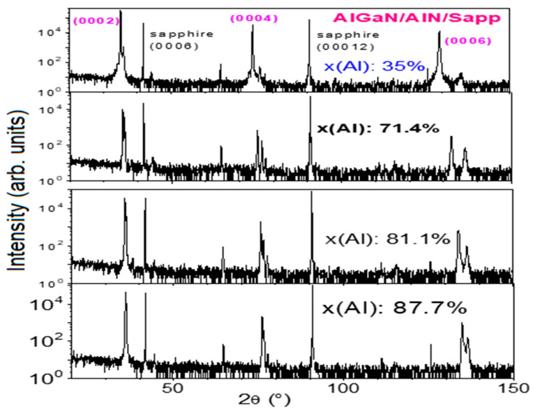
Figure 1 shows high-resolution X-ray diffraction (HR-XRD) scans of four AlGaN/AlN/sapphire samples, with the substrate sapphire (0006) peaking at 41.70° for calibration.
Figure 1.
HR-XRD wide scans of four AlGaN samples, with the substrate sapphire (0006) peak at 41.70° for calibration.
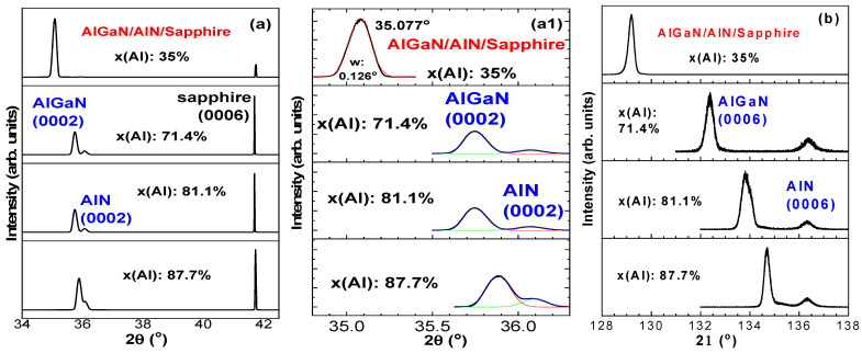
Figure 2 exhibits the first and third fine scans of four AlGaN samples. Figure 2a presents the first-order XRD fine scan with the (0002) AlGaN and AlN peaks very close, especially for high x(Al) samples. The Gaussian fittings are made in Figure 2(a1). The fitted values for AlGaN (0002) and AlN (0002) peaks and widths are A35: 35.077, 0.126; A71: 35.749, 0.129 and 36.070, 0.157; A81: 35.749, 0.129 and 36.070, 0.157; A87: 35.884, 0.137 and 36.094, 0.141, respectively, which are used for calculations in the later part of this section.
Figure 2.
HR-XRD fine scans of four AlGaN/AlN/sapphire samples. (a) The first order with the sapphire (0006) peak at 41.70° for calibration, (a1) Gaussian fits for AlGaN (0002) peaks with red lines and for AlN (0002) peaks with green lines, and (b) the third-order scans.
In addition, Figure 3 exhibits HR-XRD fine scans and Gaussian fits of the AlGaN (0006) peaks for three AlGaN samples, which are confirmed with their high x(Al) composition values of 71.4%, 81.1%, and 87.7%, respectively, from calculations below.
Figure 3.
HR-XRD fine scans and Gaussian fits of the AlGaN (0006) peaks for three AlGaN samples, with high x(Al) compositions of 71.4%, 81.1%, and 87.7%, respectively.
A set of formulas can be deduced to calculate the x(Al) for experimental samples. Based upon the Bragg rule for crystals,
| nλ = 2d sinθ | (1) |
with c = d = nλ/2sinθ, where c is the lattice constant along c-axis, λ is the X-ray wavelength of 0.154056 nm, θ the X-ray incident angle, for n = 2,
| c(GaN) = λ/sinθGaN, c(AlN) = λ/sinθAlN, and c(AlGaN) = λ/sinθAlGaN. | (2) |
As it is applied to the AlGaN lattice:
| c(AlGaN) = c(GaN) − x[c(GaN) − c(AlN)], | (3) |
using c(GaN) = 0.5185 nm, c(AlN) = 0.4978 nm [30]. We can have
| x = [c(GaN) − c(AlGaN)]/[c(GaN) − c(AlN)] = [{λ/sinθGaN} − {λ/sinθAlGaN}]/[{λ/sinθGaN} − {λ/sinθAlN}] = [{1/sinθGaN} − {1/sinθAlGaN}]/[{1/sinθGaN} − {1/sinθAlN}] |
(4) |
From XRD values of GaN with 2θGaN1(0002) = 34.60°, 2θGaN3(0006) = 126.20° [31], and AlN data with 2θAlN1(0002) = 36.10°, 2θAlN3(0006) = 136.30° [32,33], we can deduce brief calculation expressions based upon (0002) and (0006) XRD patterns as follows:
| (0002), x(Al) = 7.19 × [3.367 − (1/sinθAlGaN1)]; (0006), x(Al) = 22.7 × [1.121 − (1/sinθAlGaN3)] | (5) |
By using Equation (5) and the XRD data of (0002) and (0006) patterns, we can obtain the x(Al) values in AlxGa1−xN samples of 35.0%, 60.2%, 71.4%, 75.3%, 81.1%, and 87.7% for A35, A60, A71, A75, A81, and A87, respectively, with error bars of about ±0.2%. These values are marked in the related graphs and mentioned in Section 2. These formulas can be useful for people working in the field, although we only apply them in a limited manner in this paper.
Next, we process how to determine dislocation densities in our AlGaN layers. Referring to [14,33], the dislocation densities of AlxGa1−xN thin films can be determined by
| Dscrew = β2/(4.36b2), | (6) |
where β is the FWHM of XRD (0002) peak and b = 5.1855 Å is the Burgers vector length for the screw-type threading dislocation (TD) along the c-axis. We can calculate the screw dislocation densities of four AlGaN films with x(Al) of 35.0%, 71.4%, 81.1%, and 87.7%, listed in Table 1. It is obtained that three AlGaN films with x(Al) of 35%, 71.4%, and 81.1% have their screw dislocation densities of about 4 × 1018 cm−3, while the high x(Al) (87.7%) sample possesses a high dislocation density beyond 7 × 1018 cm−3.
Table 1.
Values of AlxGa1−xN (0002) 2θ peak/FWHM, and calculated results of screw dislocation density of four AlGaN films with x(Al) of 35.0%, 71.4%, 81.1%, and 87.7%.
| Sample Name (x%) | A35 (35.0%) | A71 (71.4%) | A81 (81.1%) | A87 (87.7%) |
|---|---|---|---|---|
| AlGaN Peak 2θ (0002) (°) | 35.077 | 35.749 | 35.749 | 35.884 |
| AlGaN FWHM 2θ (0002) (°) | 0.126 | 0.129 | 0.129 | 0.137 |
| AlGaN β: (2θFWHM*π/180, Rad) | 0.002198 | 0.002179 | 0.002179 | 0.002913 |
| AlGaN β2 (×10−6) | 4.83 | 4.75 | 4.75 | 8.49 |
| AlGaN N (×1018 cm−3) | 4.12 | 4.05 | 4.05 | 7.24 |
Note: for AlGaN, b = 0.5185 nm = 0.5185 × 10⁻⁷ cm, b2 = 0.2688 × 10⁻¹⁴ cm2, 4.36b2 = 1.172 × 10⁻¹⁴ cm2.
Further, we can calculate the screw dislocation densities of AlN layers in three AlxGa1−xN/AlN/sapphire samples with x(Al) of 71.4%, 81.1%, and 87.7%. In this case of AlN, b = 0.4982 nm [33] for calculations in Table 2.
Table 2.
Values of AlN (0002) 2θ peak/FWHM, and calculated results of screw dislocation density of three AlGaN films with x(Al) of 71.4%, 81.1%, and 87.7%.
| Sample Name (x%) | A71 (71.4%) | A81 (81.1%) | A87 (87.7%) |
|---|---|---|---|
| AlN Peak 2θ (0002) (°) | 36.070 | 36.070 | 36.094 |
| AlN FWHM 2θ (0002) (°) | 0.157 | 0.157 | 0.141 |
| AlN β: (2θFWHM*π/180, Rad) | 0.002739 | 0.002739 | 0.002460 |
| AlN β2 (×10−6) | 7.50 | 7.50 | 6.05 |
| AlN N (×1018 cm−3) | 6.93 | 6.93 | 5.59 |
Note: for AlN, b = 0.4982 nm = 0.4982 × 10⁻⁷ cm, b2 = 0.2482 × 10⁻¹⁴ cm2, 4.36b2 = 1.082 × 10⁻¹⁴ cm2.
It is obtained that three AlGaN/AlN/sapphire samples with x(Al) of 71.4%, 81.1%, and 87.7% have their AlN buffer screw dislocation densities of 6–7 × 1018 cm−3, while the high x(Al) (87.7%) sample possesses a lowest AlN dislocation density of 6 × 1018 cm−3.
3.2. Spectroscopic Ellipsometry Analysis
Variable angle (VA) spectroscopic ellipsometry (SE) measurements were conducted for five AlGaN-GaN HEMTs in the wavelength range of 193–1650 nm and with variable incident angles between 50 and 70 degrees, on each sample. Figure 4 shows typical VASE psi (Ψ) and delta (∆) spectra at 60°–70° incidences from an AlxGa1−xN sample of x = 60.2%. Through the CompleteEASE software simulation (https://www.jawoollam.com/ellipsometry-software/completeease, accessed on 29 October 2024), displayed with dotted lines for all curves in the figure, the thicknesses for AlGaN layer of 470 nm and AlN buffer/nucleation layer of 70 nm were obtained, like those reported in [27]. We employed the SE technology to deduce the relationships of refraction index n and extinction coefficient k versus wavelength λ, i.e., n~λ and k~λ, like previously for other epitaxial AlGaN [27]. In the present investigation, all AlGaN/AlN/sapphire samples were performed for SE measurements and simulations with the AlGaN layer thicknesses in the range of 400–600 nm and AlN buffer/nucleation layer thickness of 70–80 nm.
Figure 4.
Typical SE psi (Ψ) and delta (∆) spectra at 60°–70° incidences from an AlxGa1−xN sample A60 with x = 60.2%.
3.3. Raman Spectroscopy Analysis
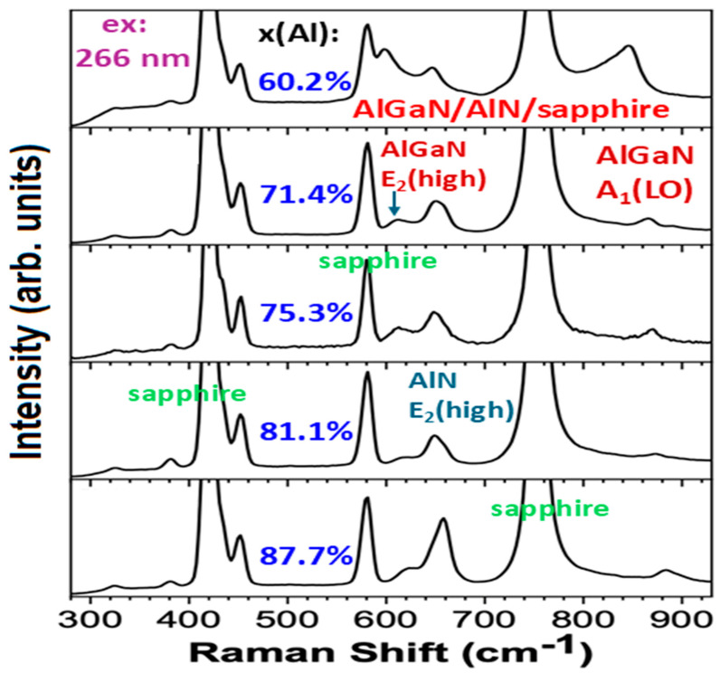
Figure 5 shows Raman scattering spectra under the 266 nm laser excitation for five AlGaN/AlN/sapphire samples with x(Al) between 60.2% and 87.7%, respectively.
Figure 5.
DUV 266 nm excitation Raman scattering spectra for 5 AlGaN/AlN/sapphire samples with high x(Al) between 60.2% and 87.7%, respectively.
As we performed the visible 532 nm excitation Raman experiments on these samples, sapphire features at 320–460 cm−1, 580 cm−1, and 750 cm−1 are extremely stronger, leading to the nitride Raman features of AlGaN E2(high), AlN E2(high), and AlGaN A1(LO) being unrecognized or weak. These difficulties can be overcome by using DUV 266 nm excitation, as observed at Figure 5, in which Raman modes of AlGaN E2(high), AlN E2(high), and AlGaN A1(LO), are well recognized. In Figure 5, on the right, between 800 cm−1 and 930 cm−1, a single mode is displayed, which is the A1(LO) mode from five AlxGa1−xN with the peak frequency varied on x(Al) from ~840 cm−1 to ~880 cm−1 as x(Al) increases from 60.2% to 87.7%.
Based upon theoretical analyses on Raman LO mode, the carrier concentrations can be calculated by way of the LO-phonon and plasma coupling (LOPC). To measure the free carrier concentration in wide bandgap semiconductors, a set of formulas on the Raman intensity of LOPC mode are presented as [30] follows:
| (7) |
| (8) |
| (9) |
In Equation (7), n1 and n2 are refractive indices at incident frequency ω1 and scattering frequency ω2, respectively; C is Faust–Henry coefficient, here the value is about 0.35; α is polarizability; E is macroscopic electric field; nω is the Bose–Einstein factor. In Equations (8) and (9), ωp is the plasma frequency, is the longitudinal optical mode frequency; is transverse optical mode frequency; η is phonon damping constant; is plasma damping constant.
Followed, the dielectric function can be described as
| (10) |
| (11) |
where ωp is the plasma frequency; n is free carrier concentration; m* is effective mass while e is unit charge; ε∞ is high frequency dielectric constant. Equation (10) of the dielectric function has been widely used in Raman studies on various semiconductors [30]. In addition, Equation (10) was employed by D.T. Talwar et al. to investigate BeTe, BexZn1−xTe, p-BeTe epilayers, and BeTe/ZnTe/GaAs superlattices [34], and GeC/Si [35].
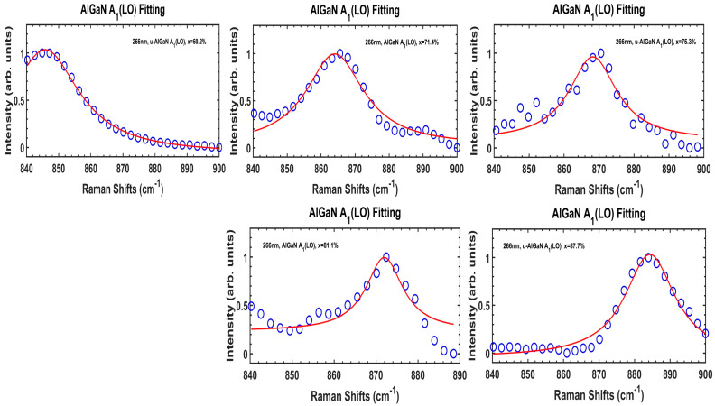
For polar semiconductors, there exists strong coupling between the LO phonon and the free carrier plasmon. By way of fitting parameter simulations, the AlGaN A1(LO) line shape in Figure 5, as the LO-phonon–plasmon coupled mode, can be fitted like that in [30], to obtain the carrier concentrations in GaN, AlN, and SiC binary semiconductors. In the present article, we applied this optical method to acquire the electronic carrier densities in ternary AlGaN compounds successfully.
Figure 6 shows fitted AlGaN A1(LO) modes from Raman scattering data (ex. 266 nm) of five AlxGa1−xN/AlN/sapphire samples with high x(Al) between 60.2% and 87.7%, respectively, by using the above Formulas (7)–(11).
Figure 6.
Fitted AlGaN A1(LO) modes from DUV 266 nm excitation Raman scattering spectra of five AlxGa1−xN/AlN/sapphire samples with high x(Al) between 60.2% and 87.7%, respectively. Fitted values and calculated results of plasmon frequency/damping constant, phonon lifetime, and carrier concentration are listed in Table 3.
Table 3.
Values of AlxGa1−xN A1(LO) peak/FWHM, and calculated results of plasmon frequency/damping constant, phonon lifetime, and carrier concentration of five AlGaN films with high x(Al) between 60.2 and 87.7%.
| Sample Name (x%) | A60 (60.2%) | A71 (71.4%) | A75 (75.3%) | A81 (81.1%) | A87 (87.7%) |
|---|---|---|---|---|---|
| A1(LO) peak (cm−1) | 845.77 | 864.05 | 868.25 | 871.98 | 884.32 |
| A1(LO) FWHM (cm−1) | 25.88 | 20.82 | 16.67 | 10.64 | 17.26 |
| ωp (THz) | 0.159 | 0.163 | 0.164 | 0.164 | 0.167 |
| γp (THz) | 4.88 | 3.92 | 3.14 | 2.01 | 3.25 |
| τphonon (ps) | 0.205 | 0.255 | 0.318 | 0.498 | 3.07 |
| Fitting Accuracy | 97.01% | 87.24% | 79.92% | 77.21% | 87.92% |
| N (×1018 cm−3) | 7.51 | 9.17 | 10.9 | 12.2 | 15.5 |
Note: ωp (plasmon frequency), γp (plasmon damping constant), τphonon (phonon lifetime), N (carrier concentration).
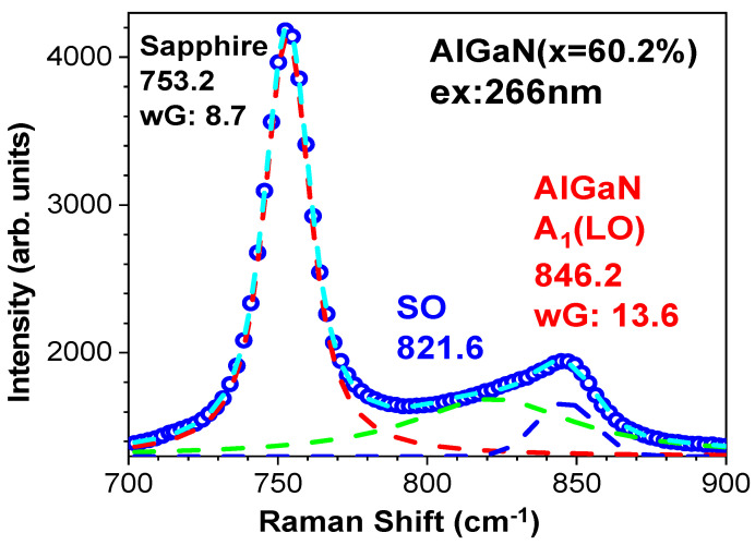
It is shown in Figure 5 that the A60 (x = 60.2%) sample has its AlGaN A1(LO) mode between 800 and 80 cm−1 with heavy asymmetric line shape. Indeed, this is indicative of an additional mode involved in the left wing of the AlGaN A1(LO) peak. A. K. Sivadasan et al. [4] demonstrated the surface optical phonon modes in hexagonal-shaped Al0.97Ga0.03N nanostructures, located below the AlGaN A1(LO) peak. Figure 7 presents Raman spectral data at 700–900 cm−1 from the A60 (x = 60.2%) sample under the 266 nm excitation, and Voigt fittings of three modes including sapphire at 753 cm−1, AlGaN A1(LO) at 846 cm−1, and the surface optical (SO) mode between them (at 822 cm−1). Because of the influence of the SO mode, our above calculations on the plasmon frequency and carrier concentration from the A60 sample could be deviated. Therefore, we repeat the fitting on the A60’s AlGaN A1(LO) mode separated from Voigt fits in Figure 7 to add into Figure 6.
Figure 7.
Raman spectral data at 700–900 cm−1 from the A60 (x = 60.2%) sample under the 266 nm excitation, and Voigt fittings of three modes of sapphire at 753 cm−1, AlGaN A1(LO) at 846 cm−1, and the surface optical (SO) mode between them (at 822 cm−1).
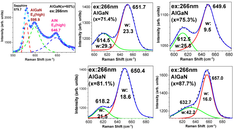
In Figure 5, between 600 cm−1 and 700 cm−1, i.e., between two strong modes at ~578 cm−1 and ~750 cm−1 from the sapphire substrate [30,33], there are two modes observed. These are the AlN E2(high) mode located at ~650 cm−1 and an AlGaN E2(high) mode with the peak frequency varied on x(Al) from ~600 cm−1 to ~630 cm−1 as x(Al) increases from 60.2% to 87.7% in five AlxGa1−xN. To investigate these two E2(high) modes in depth and clearly, we perform Voigt mode fittings on them.
Figure 8 displays these Voigt contours for five AlxGa1−xN/AlN hetero-structural samples on sapphire substrates. The A60 (x = 60.2%) sample, due to the big influence of the sapphire 580 cm−1 mode, is fitted with three Voigt modes, while the other four samples are all fitted with two Voigt mode contours. It is found that three samples with x(Al) of 71.4%, 75.3%, and 81.1% have the AlN E2(high) mode located at 650 ± 1 cm−1 only, while the A60 (x = 60.2%) sample has its AlN E2(high) mode at ~3 cm−1 lower than the standard AlN E2(high) of 650 cm−1, and the A87 (x = 87.7%) sample has its AlN E2(high) at ~7 cm−1 higher than the standard AlN E2(high) of 650 cm−1. Also, the AlGaN E2(high) mode has its peak frequency varied at 599–615–613–618–633 cm−1 as x(Al) increases from 60.2% to 87.7% in five AlxGa1−xN. These phenomena might be caused by the differences in layer axial stresses and lattice constants in AlxGa1−xN with different x(Al) amounts. This reveals that in the sample A60, the AlN buffer layer has a tensile stress, because of its AlN E2(high) with ~3 cm−1 lower than the standard AlN E2(high) value, which might be due to its larger lattice difference with the top Al0.6Ga0.4N thicker layer, while in the sample A87, the AlN buffer layer has a compressive stress, indicated by its AlN E2(high) that is ~7 cm−1 higher than the standard AlN E2(high) value.
Figure 8.
Experimental Raman (ex. 266 nm) data and Voigt mode fittings for AlGaN and AlN E2(high) modes in five AlxGa1−xN/AlN/sapphire samples with x(Al) of 60.2%, 71.4%, 75.3%, 81.1%, and 87.7%, respectively.
Our five AlxGa1−xN/AlN/sapphire samples possess AlN buffer layers (mixed with the AlN nucleation layer). By way of the spatial correlation model (SCM) analyses on AlN E2(high) modes, the Raman spectral intensity, characteristics of AlN layer quality, can be presented as
| (12) |
where q is in units of 2π/a, a is the lattice constant, L is the correlation length, indicating the phonon propagation length which characterizes the material crystalline perfection, and Г0 is the damping constant. The dispersion relation for optical phonons has an analytical form:
| ω2(q) = A + {A2 − B [1 − con(πq)]}1/2, | (13) |
| or ω(q) = A − Bq2 | (14) |
where A and B are adjustable parameters [30]. This spatial correlation model (SCM) was employed by us to investigate some semiconductors and oxides, including InGaN [36], SiC [37], InAlN [38], GaN-AlN superlattices [39], GaN/GaAs [40], and so on [30]. From Figure 5 and Figure 8, it is obvious that the AlGaN E2(high) and AlN E2(high) modes are overlapped partially for all samples and that for the A60 (x(Al) = 60.2%) sample, the AlGaN E2(high) mode is overlapped with both the sapphire 580 cm−1 mode in the left wing and the AlN E2(high) mode in the right wing. Therefore, we conduct the SCM fits on each separated E2(high) mode fitted from Voigt contours in Figure 8.
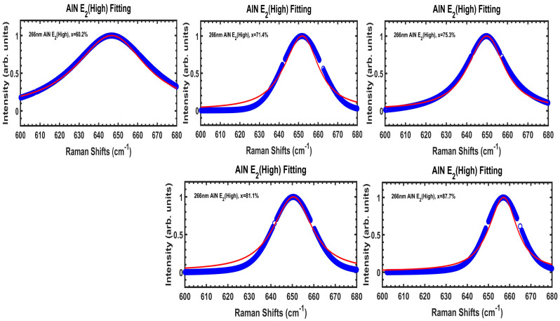
Figure 9 exhibits DUV 266 nm excitation Raman spectral information of AlN E2(high) modes, with experimental data (fitted from Voigt contours at Figure 8) in blue symbols and SCM fits by red lines, for our five AlxGa1−xN/AlN/sapphire samples. The calculated parameters based upon SCM are listed in Table 4. It is found that the correlation length L values are increasing gradually as x(Al) increases from 60.2% to 87.7%.
Figure 9.
DUV 266 nm excitation Raman spectral information of AlN E2(high) modes, with experimental data (fitted from Voigt contours at Figure 8) in blue symbols and SCM fits by red lines, for our five AlxGa1−xN/AlN/sapphire samples. The calculated parameters based upon SCM are listed in Table 2.
Table 4.
AlN E2(high) peak, FWHM, and calculated parameters based upon the spatial correlation model (SCM).
| Sample Name (x%) | A60 (60.2%) | A71 (71.4%) | A75 (75.3%) | A81 (81.1%) | A87 (87.7%) |
|---|---|---|---|---|---|
| A (cm−1) | 646.6 | 651.6 | 649.6 | 650.5 | 657.1 |
| B (cm−1) | 103 | 107 | 109 | 110 | 111 |
| L (Å) | 10 | 12 | 13 | 13.5 | 15 |
| Г0 (cm−1) | 22 | 18 | 19 | 19.5 | 20 |
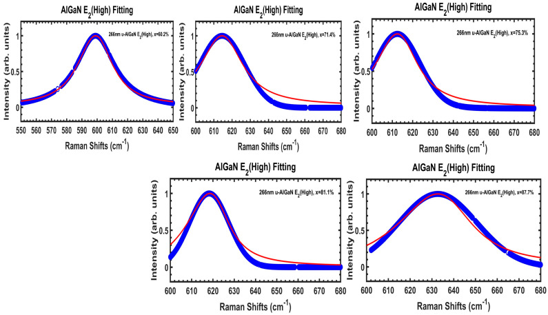
Figure 10 exhibits DUV 266 nm excitation Raman spectral information of AlGaN E2(high) modes, with experimental data (fitted from Voigt contours at Figure 8) in blue symbols and SCM fits by red lines, for five AlxGa1−xN/AlN/sapphire samples. Because the A60 (x = 60.2%) sample has its AlGaN E2(high) mode mixed with the sapphire 578 cm−1 mode, its AlGaN E2(high) mode spectrum is from Voigt fitted contours in Figure 8. The calculated parameters based upon SCM are listed in Table 5. It is found that both the correlation length L and damping constant Г0 values are gradually increased with x(Al) = 60.2% to 87.7% for these five AlxGa1−xN/AlN samples.
Figure 10.
DUV 266 nm excitation Raman spectral information of AlGaN E2(high) modes, with experimental data (fitted from Voigt contours at Figure 8) in blue symbols and SCM fits by red lines, for five AlxGa1−xN/AlN/sapphire samples. The calculated parameters based upon SCM are listed in Table 5.
Table 5.
AlGaN E2(high) peak, FWHM, and calculated parameters based upon the spatial correlation model (SCM).
| Sample Name (x%) | A60 (6.2%) | A71 (71.4%) | A75 (75.3%) | A81 (81.1%) | A87 (87.7%) |
|---|---|---|---|---|---|
| A (cm−1) | 599 | 614.7 | 614.9 | 619.2 | 638.5 |
| B (cm−1) | 108 | 108.5 | 109 | 110 | 112 |
| L (Å) | 12 | 13 | 13.5 | 14 | 14.5 |
| Г0 (cm−1) | 25 | 26 | 26.5 | 27 | 32 |
3.4. Photoluminescence Analysis
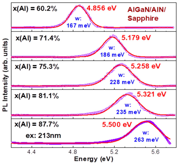
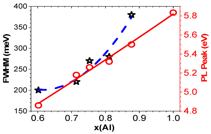
Because of tough limitations and difficulties in the experimental setup, there appear big challenges in the literature for DUV PL measurements beyond 5 eV, or shorter than 248 nm, on Al-rich AlGaN materials [6,8,9,14,41], including cathodoluminescence (CL) [12] and electroluminescence (EL) [17,18,42]. Figure 11 presents the RT photoluminescence (PL) spectra under 213 nm excitation for five AlxGa1−xN/AlN/sapphire samples with x(Al) between 60.2 and 87.7%, respectively. All PL peaks are fitted using Gaussians, with all fitted peak energy in eV and full width at half maximum (FWHM), i.e., “w: in meV”, marked inside the figure. These values are also displayed in Figure 12, in which a data point at x(Al) = 1.0 is included from an AlN/sapphire, measured under the excitation of 193 nm and reported by us in 2021 [29].
Figure 11.
RT photoluminescence (PL) spectra under 213 nm excitation for five AlxGa1−xN/AlN/sapphire samples with x(Al) between 60.2 and 87.7%, respectively.
Figure 12.
Relationships of the PL peak energy and full width at half maximum (FWHM, i.e., w in Figure 11) values vs. x(Al) for AlxGa1−xN/AlN/sapphire, in which an E peak point of x = 1.0 is from previously measured AlN/sapphire under 193 nm excitation [29]. Red open circles are for PL peaks and black stars are for FWHM. Red line and blue dashed line are guides for eye.
Figure 12 shows the relationship of PL peak energy (eV) vs. x(Al) as follows:
| EPL = 3.606 + 1.97x + 0.24x2 (eV) | (15) |
Also, the dependence of full width at half maximum (FWHM, i.e., w in Figure 11) values vs. x(Al) in Figure 12 obeys a relationship:
| W = 1119 − 3006x + 2459x 2 (meV) | (16) |
In addition, we measured RT PL spectra under the excitation of 193 nm for two AlxGa1−xN/AlN/sapphire samples, with highest x(Al) values of 81.1% and 87.7%. Compared with Figure 11 under the 213 nm excitation, the PL peak energies are slightly lower, with 25 meV and 51 meV, i.e., only 0.5% and 1%, respectively, within experimental errors. The PL band widths are narrower than 7 meV for the 81.1% sample and wider than 20 meV for the 87.7% sample, i.e., 7–8%. Therefore, these measured data under the 193 nm excitation are not shown here.
3.5. Temperature-Dependent Photoluminescence Analysis
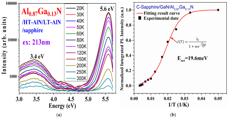
Figure 13a presents temperature-dependent photoluminescence (TDPL) spectra with variable temperature (VT) between 20 and 300 K for the Al0.87Ga0.13N/AlN/C-sapphire sample. The light-emitting peak at 5.6 eV is band-edge luminescence, and the luminescence peak at 3.4 eV may be defects-related emissions. On the main band, the relationship of normalized integrated PL intensity vs. 1/T is fitted with Arrhenius formulism, obtaining the activation energy of Eact = 19.6 meV for this sample, displayed in Figure 13b. Recently, R. Ishii et al. [43] conducted TDPL and time-resolution (TR) PL over 10–500 K for an Al0.48Ga0.52N MQW on AlN/sapphire, obtained with the radiative process activation energy of 14 meV and nonradiative process 253 meV, respectively.
Figure 13.
(a) Variable temperature (20–300 K) PL spectra of the Al0.87Ga0.13N/AlN/sapphire sample. (b) Normalized integrated PL intensity vs. 1/T, fitted with Arrhenius formulism, obtaining the activation energy of Eact = 19.6 meV.
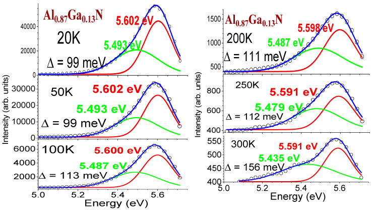
Furthermore, the main bands near 5.6 eV at Figure 13a seem asymmetrical; based upon these TDPL data (ex. 213 nm), we conducted Gaussian fits on the main PL bands at 20, 50, 100, 200, 250, and 300 K, respectively, for this Al0.87Ga0.13N/AlN/sapphire sample (displayed in Figure 14). All spectra are deconvoluted to two bands, with the strong one at 5.60–5.59 eV and the weaker one at 5.49–5.48 eV for 20–250 K, respectively. For the spectrum at 300 K, the weak intensity one is seen, with the peak at 5.435 eV.
Figure 14.
Gaussian fits on the main PL bands at 20, 50, 100, 200, 250, and 300 K, respectively, for the Al0.87Ga0.13N/AlN/sapphire sample. Each spectrum is deconvoluted to two bands, with the strong one at 5.60–5.59 eV and a weaker one at 5.49–5.48 eV for 20–250 K and at ~5.44 eV for 300 K, respectively.
3.6. Time-Resolved Photoluminescence Analysis
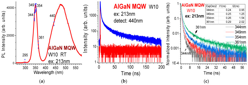
Deep ultraviolet (DUV) time-resolved photoluminescence (TRPL) spectroscopy is a powerful and attractive technology in the investigation of AlN and Al-rich AlGaN materials [44] and high x(Al) AlGaN MQWs [28,43,45,46]. J.W. Lee etc. [45] used the 266 nm pulsed laser excitation to study the PL decays from DUV LED. We established a combined photoluminescence (PL) and time-resolved photoluminescence (TRPL) spectroscopic system with deep ultraviolet (DUV) 213 nm excitation to measure AlGaN multiple quantum wells (MQWs) and related AlGaN epi-films [28,46]. Figure 15a–c show the room temperature (RT) PL and TRPL of an AlGaN MQW, W10. The RT PL of an AlGaN MQW with MQW emission peak at 350 nm, AlGaN-barrier peak at 295 nm, and a broad band over 400–580 nm is exhibited in Figure 15a. Figure 15b displays RT TRPL decay spectra from the 213 nm pulse laser (red) and the AlGaN MQW sample W10, detected at 440 nm (blue). Figure 15c presents RT TRPL decay curves, detected at four wavelengths from the AlGaN MQW sample W10. Each decay spectrum can be fitted with a double-exponential function [28,46]:
| I(t) = I10exp(−t/τ1) + I20exp(−t/τ2) | (17) |
with two carrier lifetimes of τ1 and τ2 obtained, which are listed inside the insert table of Figure 15c. It can be seen that fast decay times of 0.24–0.29 ns (10−9 s) and slow decay times of 0.95–2.0 ns are obtained. These values are comparable with those reported previously for other AlGaN MQW samples [43,45].
Figure 15.
(a) RT PL of an AlGaN MQW with MQW emission peak at 350 nm, AlGaN-barrier peak at 295 nm, and a broad band over 400–580 nm. (b) RT TRPL decay spectra from the 213 nm pulse laser (red) and the AlGaN MQW sample W10, detected at 440 nm (blue). (c) RT TRPL detected at four wavelengths for AlGaN MQW sample W10.
4. Conclusions
In summary, a series of AlxGa1−xN films with high x(Al) (60%, 71%, 75%, 81%, 87%) fractions grown on C-plane sapphire substrates with AlN nucleation layer and AlN buffer layer by metal–organic chemical vapor deposition (MOCVD) were prepared and investigated. They were initially characterized by high-resolution X-ray diffraction (HR-XRD) and Raman scattering (RS). We deduced a set of formulas for precisely determining the x(Al) in AlGaN from three orders of HR-XRD data. It was identified that DUV (266 nm) excitation RS clearly exhibits AlGaN Raman features much better than visible RS. Via Voigt fitting, the surface optical (SO) mode in the AlGaN sample with the lowest x(Al) = 60% is revealed. From the simulation on the AlGaN longitudinal optical (LO) phonon modes, the carrier concentrations of AlGaN layers in this set of high x(Al) samples were determined. The Voigt fittings separate the AlGaN and AlN E2(high) modes in overcoming their overlaps. Subsequently, the spatial correlation model (SCM) analyses were applied on the AlGaN and AlN E2(high) modes independently and probing two-layer properties. The DUV 213 nm (5.8 eV) laser was employed to study the room temperature (RT) photoluminescence (PL) and temperature-dependent photoluminescence (TDPL) properties of these high x(Al) AlxGa1−xN films with large energy gaps Eg in the range of 5.0–5.6 eV. The obtained PL bands were deconvoluted with Gaussian bands, indicating the cross-band gap emission and phonon replicas as well as variation with x(Al). TDPL spectra at 20–300 K of an Al0.87Ga0.13N exhibited the T-dependences of the band-edge luminescence near 5.6 eV and the phonon replicas. According to the Arrhenius fitting diagram of the TDPL spectra, the activation energy (19.6 meV) associated with the luminescent process was acquired. Further, the combined PL and time-resolved photoluminescence (TRPL) spectroscopic system with DUV 213 nm pulse excitation was applied to measure AlGaN multiple quantum wells (MQWs). RT TRPL decay spectra were obtained at four wavelengths and fitted by two exponentials, with fast decay times of 0.24–0.29 ns and slow decay times of 0.95–2.0 ns obtained. Comprehensive studies on the crystalline and optical properties of Al-rich AlGaN epi-films and a typical AlGaN MQW were achieved with unique and significant results, which provides useful references to growers and investigators in the III-nitrides and other materials fields.
Author Contributions
Conceptualization, Z.C.F. and X.Z.; data collection, M.T., M.T.N. and Z.C.F.; supervision, X.Z., B.K. and I.F.; data curation, Z.C.F., M.T., M.T.N., Y.L. and J.Y.; data analysis, Z.C.F., M.T., M.T.N., Y.L. and J.Y.; investigation, Z.C.F., M.T. and M.T.N.; writing—original draft preparation, Z.C.F., M.T. and M.T.N.; writing—review and editing, Z.C.F. and M.T.N.; project administration, X.Z., B.K. and I.F.; funding acquisition, X.Z. and I.F. All authors have read and agreed to the published version of the manuscript.
Data Availability Statement
The data presented in this study are available on request from the corresponding author.
Conflicts of Interest
The authors declare no conflicts of interest.
Funding Statement
This work was supported by National Natural Science Foundation of China (No. 61367004, No. 61964002); Key Research and Development Project of Science and Technology Department of Jiangsu Province, China (grant No. BE2021008-4); Guangxi Natural Science Foundation (2018GXNSFAA138127).
Footnotes
Disclaimer/Publisher’s Note: The statements, opinions and data contained in all publications are solely those of the individual author(s) and contributor(s) and not of MDPI and/or the editor(s). MDPI and/or the editor(s) disclaim responsibility for any injury to people or property resulting from any ideas, methods, instructions or products referred to in the content.
References
- 1.Feng Z.C., editor. Handbook of Solid-State Lighting and LEDs. CRC Press, Taylor & Francis Group; Boca Raton, FL, USA: 2017. p. 705. Chapter 24. [DOI] [Google Scholar]
- 2.Chu R., Shinohara K., editors. III-Nitride Electronic Devices. Academic Press; Cambridge, MA, USA: 2019. ISBN 10: 0128175443, ISBN 13: 9780128175446. [Google Scholar]
- 3.Hao Y., Zhang J.-F., Zhang J.-C., editors. Nitride Wide Bandgap Semiconductor Material and Electronic Devices. CRC Press; Boca Raton, FL, USA: 2020. ISBN 10: 0367574365, ISBN 13: 9780367574369. [Google Scholar]
- 4.Sivadasan A.K., Singha C., Raghavendra K.G., Amirthapandian S., Bhattacharyya A., Dasgupta A., Dhara S. Surface optical phonon modes in hexagonal shaped Al0.97Ga0.03N nanostructures. Appl. Phys. A. 2017;123:527. doi: 10.1007/s00339-017-1139-3. [DOI] [Google Scholar]
- 5.Bokhana P.A., Fateeva N.V., Malina T.V., Osinnykha I.V., Zakrevsky D.E., Zhuravlev K.S. Luminescence properties of heavily doped AlxGa1-xN/AlN films grown on sapphire substrate. J. Lumin. 2018;203:127–134. doi: 10.1016/j.jlumin.2018.06.034. [DOI] [Google Scholar]
- 6.Reddy P., Breckenridge M.H., Guo Q., Klump A., Khachariya D., Pavlidis S., Mecouch W., Mita S., Moody B., Tweedie J., et al. High gain, large area, and solar blind avalanche photodiodes based on Al-rich AlGaN grown on AlN substrates. Appl. Phys. Lett. 2020;116:081101. doi: 10.1063/1.5138127. [DOI] [Google Scholar]
- 7.Foronda H.M., Hunter D.A., Pietsch M., Sulmoni L., Muhin A., Graupeter S., Susilo N., Schilling M., Enslin J., Irmscher K., et al. Electrical properties of (11-22) Si:AlGaN layers at high Al contents grown by metal-organic vapor phase epitaxy. Appl. Phys. Lett. 2020;117:221101. doi: 10.1063/5.0031468. [DOI] [Google Scholar]
- 8.Lee K., Page R., Protasenko V., Schowalter L.J., Toita M., Xing H.G., Jena D. MBE growth and donor doping of coherent ultrawide bandgap AlGaN alloy layers on single-crystal AlN substrates. Appl. Phys. Lett. 2021;118:092101. doi: 10.1063/5.0037079. [DOI] [Google Scholar]
- 9.Mondal S., Wang D., Anhar A.F.M., Bhuiyan U., Hu M., Reddeppa M., Wang P., Zhao H., Mi Z. Tunable bandgap and Si-doping in N-polar AlGaN on C-face 4H-SiC via molecular beam epitaxy. Appl. Phys. Lett. 2023;123:182106. doi: 10.1063/5.0173637. [DOI] [Google Scholar]
- 10.Rathkanthiwar S., Reddy P., Quiñones C.E., Loveless J., Kamiyama M., Bagheri P., Khachariya D., Eldred T., Moody B., Mita S., et al. Anderson transition in compositionally graded p-AlGaN. J. Appl. Phys. 2023;134:195705. doi: 10.1063/5.0176419. [DOI] [Google Scholar]
- 11.Majchrzak D., Tran L., Babij M., Serafińczuk J., Olszewski W., Kuna R., Opołczyńska K., Piejko A., Michałowski P., Kudrawiec R., et al. Thickness and Mg doping of graded AlGaN layers: Influence on contact layer’s structural and electrical properties for DUV emitters. Mater. Sci. Semicond. Process. 2024;178:108452. doi: 10.1016/j.mssp.2024.108452. [DOI] [Google Scholar]
- 12.Wang J.M., Xu F.J., Zhang L.S., Lang J., Fang X.Z., Zhang Z.Y., Guo X.Q., Ji C., Ji C.Z., Tan F.Y., et al. Progress in efficient doping of Al-rich AlGaN. J. Semicond. 2024;45:021801. doi: 10.1088/1674-4926/45/2/021501. [DOI] [Google Scholar]
- 13.Yamada R., Kondo R., Miyake R., Nishibayasi T., Matsubara E., Imoto Y., Iwayama S., Takeuchi T., Kamiyama S., Miyake H., et al. Homoepitaxial Regrowth of AlGaN on AlGaN Templates Prepared via Chemical Mechanical Polishing and Its Application to UV-B Laser Diodes. Phys. Status Solidi A. 2024:2400113. doi: 10.1002/pssa.202400113. [DOI] [Google Scholar]
- 14.Wei W., Yang Y., Peng Y., Maraj M., Sun W. Optical and Electrical Properties of AlxGa1−xN/GaN Epilayers Modulated by Aluminum Content. Molecules. 2024;29:1152. doi: 10.3390/molecules29051152. [DOI] [PMC free article] [PubMed] [Google Scholar]
- 15.Lu S.P., Bai J.X., Li H.B., Jiang K., Ben J.W., Zhang S.L., Zhang Z.H., Sun X.J., Li D.B. 240 nm AlGaN-based deep ultraviolet micro-LEDs: Size effect versus edge effect. J. Semicond. 2024;45:012504. doi: 10.1088/1674-4926/45/1/012504. [DOI] [Google Scholar]
- 16.Ishii R., Tanaka S., Susilo N., Wernicke T., Kneissl M., Funato M., Kawakami Y. Radiative and Nonradiative Recombination Processes in AlGaN Quantum Wells on Epitaxially Laterally Overgrown AlN/Sapphire from 10 to 500 K. Phys. Status Solidi B. 2024:2400018. doi: 10.1002/pssb.202400018. [DOI] [Google Scholar]
- 17.Liu X., Xu S., Tao H., Cao Y., Wang X., Shan H., Zhang J., Hao Y. High Efficiency Deep Ultraviolet Light-emitting Diodes with Polarity Inversion of Hole Injection Layer. IEEE Photonics J. 2023;15:8200205. doi: 10.1109/JPHOT.2023.3247451. [DOI] [Google Scholar]
- 18.Liu X., Lv Z., Liao Z., Sun Y., Zhang Z., Sun K., Zhou Q., Tang B., Geng H., Qi S., et al. Highly efficient AlGaN-based deep-ultraviolet lightemitting diodes: From bandgap engineering to device craft. Microsyst. Nanoeng. 2024;10:110. doi: 10.1038/s41378-024-00737-x. [DOI] [PMC free article] [PubMed] [Google Scholar]
- 19.Zhang Z., Yoshikawa A., Kushimoto M., Aoto K., Sasaoka C., Amano H. Impact of unintentionally formed compositionally graded layer on carrier injection efficiency in AlGaN-based deep ultraviolet laser diodes. Appl. Phys. Lett. 2024;124:061109. doi: 10.1063/5.0184543. [DOI] [Google Scholar]
- 20.Carey IV P.H., Ren F., Bae J., Kim J., Pearton S.J. Proton Irradiation of High Aluminum Content AlGaN Polarization Doped Field Effect Transistors. ECS J. Solid State Sci. Technol. 2020;9:025003. doi: 10.1149/2162-8777/ab71f0. [DOI] [Google Scholar]
- 21.Baca A.G., Armstrong A.M., Klein B.A., Allerman A.A., Douglas E.A., Kaplar R.J. Al-rich AlGaN based transistors. J. Vac. Sci. Technol. A. 2020;38:020803. doi: 10.1116/1.5129803. [DOI] [Google Scholar]
- 22.Klein B.A., Allerman A.A., Baca A.G., Nordquist C.D., Armstrong A.M., Van Heukelom M., Rice A., Patel V., Rosprim M., Caravello L., et al. AlGaN High Electron Mobility Transistor for High-Temperature Logic. J. Microelectron. Electron. Packag. 2023;20:1–8. doi: 10.4071/imaps.1832996. [DOI] [Google Scholar]
- 23.Bassaler J., Mehta J., Abid I., Konczewicz L., Juillaguet S., Contreras S., Rennesson S., Tamariz S., Nemoz M., Semond F., et al. Al-Rich AlGaN Channel High Electron Mobility Transistors on Silicon: A Relevant Approach for High Temperature Stability of Electron Mobility. Adv. Electron. Mater. 2024:2400069. doi: 10.1002/aelm.202400069. [DOI] [Google Scholar]
- 24.Papamichail A., Persson A.R., Richter S., Stanishev V., Armakavicius N., Kühne P., Guo S., Persson P.O.Å., Paskov P.P., Rorsman N., et al. Impact of Al profile in high-Al content AlGaN/GaN HEMTs on the 2DEG properties. Appl. Phys. Lett. 2024;125:123505. doi: 10.1063/5.0218911. [DOI] [Google Scholar]
- 25.Du H., Hao L., Liu Z., Song Z., Zhang Y., Dang K., Zhou J., Ning J., Li Z., Zhang J., et al. High-Al-composition AlGaN/GaN MISHEMT on Si with fT of 320 GHz. Sci. China Inf. Sci. 2024;67:169402. doi: 10.1007/s11432-024-3998-2. [DOI] [Google Scholar]
- 26.Chen S., Zhang X., Fan A., Chen H., Li C., Feng Z.C., Lyu J., Zhuang Z., Hu G., Cui Y. Characterization of optical properties and thermo-optic effect for non-polar AlGaN thin films using spectroscopic ellipsometry. J. Phys. D Appl. Phys. 2020;53:205104. doi: 10.1088/1361-6463/ab77e2. [DOI] [Google Scholar]
- 27.Liu Y., Li Q.X., Wan L.Y., Kucukgok B., Ferguson I.T., Zhang X., Feng Z.C., Lu N. Composition and Temperature Dependent Optical Properties of AlxGa1−xN alloy by Spectroscopic Ellipsometry. Appl. Surf. Sci. 2017;421:389–396. doi: 10.1016/j.apsusc.2017.01.309. [DOI] [Google Scholar]
- 28.Guo W., Chen L., Xu H., Qian Y., Sheikhi M., Hoo J., Guo S., Xu L., Liu J., Alqatari F., et al. Revealing the surface electronic structures of AlGaN deep ultraviolet multiple-quantum-wells with lateral polarity domains. Photonics Res. 2020;8:812–818. doi: 10.1364/PRJ.387700. [DOI] [Google Scholar]
- 29.Yin J., Chen D., Yang H., Liu Y., Talwar D.N., He T., Ferguson I.T., He K., Wan L., Feng Z.C. A comparative study of multiple spectroscopies for AlN thin films grown on sapphire and 6H-SiC by metal organic chemical vapor deposition. J. Alloys Compd. 2021;857:157487. doi: 10.1016/j.jallcom.2020.157487. [DOI] [Google Scholar]
- 30.Feng Z.C. Raman Scattering on Emerging Semiconductors and Oxides. CRC Press; London, UK: Taylor & Francis Group; New York, NY, USA: 2024. [(accessed on 1 September 2024)]. p. 180. Chapter 9. Available online: www.routledge.com/9781032638874. [Google Scholar]
- 31.Pushkareva S.S., Grekhovb M.M., Zenchenko N.V. X-Ray Diffraction Analysis of Features of the Crystal Structure of GaN/Al0.32Ga0.68N HEMT-Heterostructures by the Williamson–Hall Method. Semiconductors. 2018;52:734–738. doi: 10.1134/S1063782618060209. [DOI] [Google Scholar]
- 32.Endo Y., Sato T., Takita A., Kawamura Y., Yamamoto M. Magnetic, Electrical Properties, and Structure of Cr–AlN and Mn–AlN Thin Films Grown on Si Substrates. IEEE Trans. Magn. 2005;41:2718–2720. doi: 10.1109/TMAG.2005.854686. [DOI] [Google Scholar]
- 33.Wei W., Peng Y., Yang Y., Xiao K., Maraj M., Yang J., Wang Y., Sun W. Study of Defects and Nano-patterned Substrate Regulation Mechanism in AlN Epilayers. Nanomaterials. 2022;12:3937. doi: 10.3390/nano12223937. [DOI] [PMC free article] [PubMed] [Google Scholar]
- 34.Talwar D.N., Becla P. Assessment of optical phonons in BeTe, BexZn1-xTe, p-BeTe epilayers and BeTe/ZnTe/GaAs (001) superlattices. Appl. Phys. A. 2022;128:702. doi: 10.1007/s00339-022-05819-z. [DOI] [Google Scholar]
- 35.Talwar D.N., Haraldsen J.T. Simulations of Infrared Reflectivity and Transmission Phonon Spectra for Undoped and Doped GeC/Si (001) Nanomaterials. 2024;14:1439. doi: 10.3390/nano14171439. [DOI] [PMC free article] [PubMed] [Google Scholar]
- 36.Sugiura T., Kawaguchi Y., Tsukamoto T., Andoh H., Yamaguchi M., Hiramatsu K. Raman Scattering Study of InGaN Grown by Metalorganic Vapor Phase Epitaxy on (0001) Sapphire Substrates. Jpn. J. Appl. Phys. 2001;40:5955–5958. doi: 10.1143/JJAP.40.5955. [DOI] [Google Scholar]
- 37.Havel M., Baron D., Colomban P. ‘Smart’ Raman/Rayleigh imaging of nanosized SiC materials using the spatial correlation model. J. Mater. Sci. 2004;39:6183–6190. doi: 10.1023/B:JMSC.0000043585.29016.5a. [DOI] [Google Scholar]
- 38.Katsikini M., Arvanitidis J., Christofilos D., Ves S., Adikimenakis A., Georgakilas A. Raman scattering of InxAl1-xN alloys with 0.2 < x < 0.9. Phys. Status Solidi C. 2010;7:76–79. doi: 10.1002/pssc.200982607. [DOI] [Google Scholar]
- 39.Rodrigues A.D., de Godoy M.P.F., Mietze C., As D.J. Phonon localization in cubic GaN/AlN superlattices. Solid State Commun. 2014;186:18–22. doi: 10.1016/j.ssc.2014.01.012. [DOI] [Google Scholar]
- 40.Ning J.Q., Zheng C.C., Zheng L.X., Xu S.J. Beyond spatial correlation effect in micro-Raman light scattering: An example of zinc-blende GaN/GaAs hetero-interface. J. Appl. Phys. 2015;118:073101. doi: 10.1063/1.4928618. [DOI] [Google Scholar]
- 41.Liu B., Xu F., Wang J., Lang J., Wang L., Fang X., Yang X., Kang X., Wang X., Qin Z., et al. Correlation between electrical properties and growth dynamics for Si-doped Al-rich AlGaN grown by metal-organic chemical vapor deposition. Micro Nanostructures. 2022;163:107141. doi: 10.1016/j.spmi.2021.107141. [DOI] [Google Scholar]
- 42.Li D., Liu S., Qian Z., Liu Q., Zhou K., Liu D., Sheng S., Sheng B., Liu F., Chen Z., et al. Deep-Ultraviolet Micro-LEDs Exhibiting High Output Power and High Modulation Bandwidth Simultaneously. Adv. Mater. 2022;34:2109765. doi: 10.1002/adma.202109765. [DOI] [PubMed] [Google Scholar]
- 43.Zhao J., Zhang X., He J., Chen S., Fan A., Pan J., Chen D., Feng Z.C., Sun Q., Chang J., et al. Improved optical properties of nonpolar AlGaN-based multiple quantum wells emitting at 280 nm. IEEE Photonics J. 2021;13:2300107. doi: 10.1109/JPHOT.2020.3039897. [DOI] [Google Scholar]
- 44.Shigefusa F. Chichibu, Takeyoshi Onuma, Kouji Hazu, and Akira Uedono, Time-resolved luminescence studies on AlN and high AlN mole fraction AlGaN alloys. Phys. Status Solidi C. 2013;10:501–506. doi: 10.1002/pssc.201200676. [DOI] [Google Scholar]
- 45.Lee J.W., Ha G., Park J., Song H.G., Park J.Y., Lee J., Cho Y.-H., Lee J.-L., Kim J.K., Kim J.K. AlGaN Deep-Ultraviolet Light-Emitting Diodes with Localized Surface Plasmon Resonance by a High-Density Array of 40 nm Al Nanoparticles. ACS Appl. Mater. Interfaces. 2020;12:36339–36346. doi: 10.1021/acsami.0c08916. [DOI] [PubMed] [Google Scholar]
- 46.Shan M., Zhang Y., Tian M., Lin R., Jiang J., Zheng Z., Zhao Y., Lu Y., Feng Z.C., Guo W., et al. Transverse Electric Lasing at a Record Short Wavelength 244.63 nm from GaN Quantum Wells with Weak Exciton Localization. ACS Photonics. 2021;8:1264–1270. doi: 10.1021/acsphotonics.1c00090. [DOI] [Google Scholar]
Associated Data
This section collects any data citations, data availability statements, or supplementary materials included in this article.
Data Availability Statement
The data presented in this study are available on request from the corresponding author.


