

Abstract
In planar superconducting circuits, decoherence due to materials imperfections, especially two-level-system (TLS) defects at different interfaces, is a primary hurdle for advancing quantum computing and sensing applications. Traditional methods for mitigating TLS loss, such as etching oxide layers at metal and substrate interfaces, have proven to be inadequate due to the persistent challenge of oxide regrowth. In this work, we introduce a novel approach that employs molecular self-assembled monolayers (SAMs) to chemically bind at different interfaces of superconducting circuits. This technique is specifically tested here on coplanar waveguide (CPW) resonators, in which this method not only impedes oxide regrowth after surface etching but can also tailors the dielectric properties at different resonators interfaces. The deployment of SAMs results in a consistent improvement in the measured quality factors across multiple resonators, surpassing those with only oxide-etched resonators. The efficiency of our approach is supported by microwave measurements of multiple devices conducted at millikelvin temperatures and correlated with detailed X-ray photoelectron spectroscopy (XPS) and transmission electron microscopy (TEM) characterizations of SAM-passivated resonators. The compatibility of SAMs materials with the established fabrication techniques offers a promising route to improve the performance of superconducting quantum devices.
Subject terms: Surfaces, interfaces and thin films; Qubits
Introduction
Superconducting circuits serve as key components in constructing circuit quantum electrodynamics (cQED) systems. Over the past two decades and among different platforms for quantum computing, superconducting qubits have emerged as a promising avenue due to improvements in coherence times and gate fidelities1–3. Qubits are nonlinear LC oscillators and form the basic units of quantum information, while resonators are harmonic LC oscillators used mainly for addressing the states of qubits4,5, qubit-qubit coupling6,7 and quantum memory8,9. In practical devices, qubits and resonators are typically coupled to each other, forming a complex network of interaction that is crucial for performing quantum information processing. However, the construction of large and functional quantum devices necessitates substantial improvements in qubit relaxation and coherence times, which are currently orders of magnitude shorter than the thresholds imposed by constituent materials. At millikelvin temperatures and single-photon power excitations, materials loss in both qubits and resonators are predominantly attributed to a photon in the system being frequently coupled to a two-level system (TLS) that can exist inside bulk materials and at different interfaces, which is currently more prominently attributed to the presence of oxides at air-interfaces of metal and substrate10. Oxides related TLS loss are therefore recognized as a significant decoherence channel in quantum circuits, impacting both small features of Josephson junctions and large features of circuits’ capacitors and inductors of both qubits and resonators10–12.
Central to numerous superconducting qubit architectures, coplanar waveguide (CPW) resonators are pivotal components that also serve as standalone tools for characterizing materials’ loss under microwave single-photon excitations10,13,14. Efforts have been directed toward modifying resonator geometries12,15 and trying different materials16–18 to comprehend and diminish TLS loss that can exist in metal-air (MA), metal-substrate (MS), and substrate-air (SA) interfaces. Despite ongoing debates about the origin of TLS loss11, it is currently believed that such deleterious systems primarily stem from defects at these three interfaces19,20. It is also suspected that TLS loss might be present at interfaces containing chemical residues from the fabrication process and other sources11,15. Defects tend to manifest mainly in disordered, both structurally and chemically, materials at air-interfaces and efforts have been undertaken to comprehend and mitigate these issues11,21. While the MS interface can be ameliorated through substrate cleaning and improved epitaxial film growth16,22–24, addressing oxide growth at air-interfaces proves to be more challenging due to inherent materials properties of these amorphous layers. A previous report demonstrated a substantial improvement in resonators’ quality factors through chemically etching oxides present at MA and SA interfaces25. Nonetheless, the reformation of oxides after etching remains a persistent challenge for sustaining the improved quality factors. Approaches like self-limiting oxide growth26, nitrogen plasma treatments27 and surface encapsulation28 offer potential solutions for oxides regrowth. Recently, we presented preliminary outcomes related to the absorption of Octatrichlorosilane (OTS) self-assembled monolayers on Si and Nb surfaces, exploring their impact on oxide regrowth29. In this article, we delve into a detailed study involving other types of SAM materials absorbed on metal and substrate surfaces, investigating their role in suppressing oxide regrowth and improving the dielectric constants of MA and SA interfaces.
The ability to form a wide range of molecular SAMs on metallic/semiconducting surfaces through various processes, such as from a dip into evaporation-based deposition, is an attractive proposition30,31. Over the last three decades, SAMs absorbed onto diverse metallic and semiconducting surfaces have allowed to finely tune the physical and chemical properties of various interfaces32–35. This extends to the realms of molecular, organic, and conventional electronics, where SAMs play roles as electronic components and in controlling surface attributes such as work function and dielectric properties35. The suppression of oxide growth on semiconducting metal and oxide surfaces through SAMs absorption is a well-explored phenomenon36,37. Given that oxides present at various air-interfaces harbor structural and chemical defects, they are a major source of decoherence in quantum devices11,19,20, as these oxides foster TLS defects. SAMs at MA- and SA-interfaces can replace these defects with materials devoid of chemical and structural imperfections. Consequently, SAMs not only impede oxide regrowth but also substantially reduce undesired energy absorption in these additional layers due to their well-established defect-free structural and electronic characteristics38,39. The robust chemical bonding of SAMs at air-interfaces, determined by the binding ends of SAMs with the metal and substrate chemical structure, defines the crystal structure of the bonded SAM material, a phenomenon well-documented across various interfaces30,31. Defect-free SAM assembly on a smooth surface possesses the ability to minimize TLS loss to a very low level. Moreover, the dielectric constant of oxides at different device interfaces plays a crucial role in TLS loss mechanisms, and SAMs can be harnessed to control such loss since these materials have been demonstrated to modify surface dielectric properties, such as within a broad range of 2–20 dielectric constants40–42.
Recent theoretical and experimental results have demonstrated SAM-based modification of the dielectric constants of semiconductor/metal-oxide surfaces41, although studies focusing on loss tangents for such SAM-modified surfaces remain unexplored. Similar to recent reports42, superconducting CPW resonators provide a suitable platform for studying the dielectric constant and loss tangent of SAMs. Notably, SAMs materials are highly compatible with many established micro-/nano-fabrication processes43, making these materials feasible to be used at various stages of the fabrication process of superconducting devices. Additionally, the incorporation of SAM-based sandwich structures, featuring conducting and non-conducting SAMs, is commonplace in molecular electronics44,45. Thus, in addition to reducing surface losses in superconducting devices, SAMs could potentially be employed as well to mitigate losses in the fabrication of Josephson junctions when combined with a suitable insulating SAM layer.
In this work, we show the passivation of CPW resonators using molecular self-assembled monolayers on Nb and Si surfaces, including MA- and SA-interfaces, which results in a sustained improvement over time in the quality factors of multiple treated devices. This observation is supported by analytical scanning transmission electron microscopy (STEM), X-ray photoemission spectroscopy (XPS) and atomic force microscopy (AFM) measurements, in which all of these measurements collectively indicate the mitigation of TLS loss as a result of the uniform SAMs passivation of metal and substrate surfaces.
Results and discussion
Device design and the STEM images are shown in Fig. 1a,b, respectively, illustrating CPW structures and the targeted areas for materials analysis. The cross-sectional STEM images (Fig. 1c,d) are particularly revealing, highlighting the stark contrast between untreated and SAM-treated surfaces in which this provides intricate nanometer-resolution EDS fluorescence mappings of the impact of self-assembled monolayers on oxide growth through illustrating elemental compositions and chemical states of the three resonator interfaces (MA, SA, and MS). In the untreated sample (Fig. 1c), a pronounced contrast of oxides at the MA interfaces is clearly present, consistent with expected oxide regrowth after post-fabrication BOE etching when the sample is exposed to ambient environment. These oxides at device interfaces are what to contribute significantly to TLS loss. In contrast, the SAM-treated sample after BOE etching (Fig. 1d) shows a markedly reduced oxide presence and more color-contrasted Nb and Si signals. This observation in STEM-EDS mappings shows elemental composition and provides an illustration of the reduced oxide growth on SAM-treated MA and SA interfaces.
Figure 1.

Resonators device and EDS colored STEM images of MA, MS and SA interfaces 20 days after fabrication and SAM treatment. (a) A 10 mm 10 mm chip of resonators device in a sample box, featuring ten Nb CPW patterns on a Si substrate. (b) SEM images of a single resonator indicating the locations from which TEM cross-sectional lamella were extracted. Cross-sectional EDS-STEM images of different interfaces after post-fabrication BOE etching of MA and SA interfaces in which (c) is a sample without SAM treatment and (d) shows a treated sample with a double-layered SAMs adsorption of both OTS and MPA.
Remarkably, our high-resolution STEM-EDS images also indicate that the grown layer of oxide on the MA interface has the ability to dissipate through the metal surface, impacting not only the MA interface but also the bulk dielectrics. Whereas in the crystalline material of Si substrate, oxides are not observed to be present inside the bulk material but only at the SA interface. This observation is clearly shown in Fig. 1c of the untreated sample, whereas the SAM-treated sample in Fig. 1d indicates significantly less amount of oxides both at the MA interface and inside the bulk material of Nb. The reason behind this observation is anticipated to be that SAM binds through a layer of oxygen atoms to the metal surface, which implies that there are no additional oxides except at the binding ends of the specific SAM molecule, which prevents further dissipation of oxide formation from the interface down to the bulk material. Our specific case necessitates further in-depth investigation into the concurrent binding of the double-layered OTS-MPA onto the Nb and Si surfaces, and how this dual-binding of SAMs molecules influences oxide penetration on the Nb thin film. In addition, the temporal aspect of these observations is critical as well, in which these imaging data were collected 20 days post-sample fabrication and preparation, a period sufficiently long for oxides to typically form. This time-dependent analysis is pivotal, as it confirms the lasting effectiveness of SAM treatment against oxide formation, a process that usually occurs rapidly in untreated conditions.
Additionally, XPS measurements are shown in Fig. 2 obtained for Si and Nb air-interfaces subjected to different surface treatments, both for BOE etched resonators and for various SAMs treated resonators. Subsequent to BOE etching, all SAMs treated samples were promptly passivated with SAMs materials, with the detailed process described in the methods section.29. We obtained XPS data twice for each sample including for both fresh devices and for aged devices after 20 days of sample preparation and before XPS measurements in order to validate the effectiveness of SAMs surface treatments over time. Moreover, XPS measurements of Nb surfaces (Fig. 1a,b) exhibit a more pronounced suppression of Nb oxide peaks in the spectra of SAM passivated samples as compared to samples solely etched with BOE, both in the case of fresh and aged samples. Both OTS and MPA have proven effective in restraining oxide regrowth on Nb after sufficient BOE etching. These SAMs molecules have a propensity to bind at minimum oxidized surfaces35 with extensive validation for SAM bonding on materials like silicon, copper, aluminum and palladium, in comparison to niobium36,37. Remarkably, the simultaneous adsorption of double-layered OTS-MPA on Nb has shown to be effective, while the maximal suppression of Nb oxide peaks happened in the treatment with OTS for both cases of fresh and aged devices.
Figure 2.

XPS analysis of Si and Nb surfaces after BOE etching and SAM passivation with OTS, MPA and double-layered OTS-MPA. XPS spectra of Nb surfaces for (a) fresh devices and (b) aged devices. XPS spectra of Si surfaces for (c) fresh devices and (d) aged devices. Even after 20 days, the amount of Nb and Si oxides in the SAMs treated samples is observed to be lower than the samples only etched with BOE.
In the case of Si XPS spectra (Fig. 1c,d), both Si 2s and 2p loss peaks were attenuated following SAMs treatments in the case of fresh and aged samples. Notably, Si 2s and 2p peaks exhibited maximal intensity in the case of fresh BOE etched sample (Fig. 1c), yet these peaks significantly decreased in the case of the aged BOE etched sample due to oxide growth on Si surface (Fig. 1d). Furthermore, XPS data demonstrated a reduction in Si loss peaks attributed to energy loss (plasmon) effects subsequent to BOE cleaning. In stark contrast, SAM passivation led to a further reduction in plasmon peaks for both fresh and aged samples. The profile of Si 2s and 2p plasmon loss peaks is influenced by the materials traversed by the photoelectrons, and these loss structures can potentially interfere with the interpretation and quantification of other spectral peaks, such as the Si 2s and 2p signals in this context.
In this work, data was measured for ten CPW resonators in multiple devices for different surface treatments. Detailed microwave measurements at single-photon regime are shown in Fig. 3 for various cases. Microwave signals for fresh and aged devices are shown in Fig. 4a,b, respectively, where the decreased peak’s depth at resonance indicates reduced loss at MA and SA interfaces due to SAMs passivation. In both cases, SAMs treated resonators indicate less transmission loss in the spectrum of measured signal. Detailed measurements across all resonators for multiple freshly treated devices are shown in Fig. 4c, in which values for SAMs treated resonators surpass most of only BOE-etched resonators. The average across each device indicate resonators treated with both OTS and double-layered OTS-MPA achieved more than a factor of two improvement over multiple resonators. Furthermore, the observed improvement in due to SAMs treatments is indicative of a substantial reduction in the dielectric loss due to mitigation of TLS loss at MA and SA interfaces. The data suggests that the molecular layers introduced by the SAM treatments create a more favorable interface for the resonator, thus enhancing the coherence and reducing the energy dissipation in these systems.
Figure 3.

Microwave reflectometry measurements comparing the performance of resonators with different surface treatments. Measurements of single resonators in fresh BOE-etched and SAM-passivated samples are shown in (a), while aged BOE-etched and SAM-passivated samples are shown in (b). Detailed resonators measurements across each fresh device is shown in (c) with average over each device shown in the inset figure. All measurements were conducted at single-photon input power. Both OTS and double-layered OTS-MPA treatments achieved comparable high average across multiple resonators.
Figure 4.

Power and Temperature dependent measurements of resonators in multiple device with different surface treatments. Resonator intrinsic loss as function of average photon number for fresh and aged devices in (a) and (b), respectively. Resonator intrinsic loss as function of temperature for fresh and aged devices in (c) and (d). For both fresh and aged devices, OTS-treated resonators show minimal intrinsic loss.
The power- and temperature- dependent results in Fig. 4 offer comprehensive measurements of resonators intrinsic loss, denoted as , across a spectrum of operational conditions for devices with various surface treatments. Panels (a) and (b) delineate the dependency of on the average photon number for fresh and aged devices, respectively. It is evident that in both temporal states, the resonators that have undergone SAM treatment manifest a markedly lower intrinsic loss compared to those subjected solely to BOE etching . This discrepancy in loss is particularly pronounced at low photon numbers, suggesting that the SAMs passivation serves as an effective barrier, mitigating the impact of TLS loss, which are known to be predominant at these energy scales. The consistency of this effect across both fresh and aged devices shows the robustness of SAMs surface treatments in preserving the integrity of the resonator surfaces over time.
Moving to the temperature dependency illustrated in panels (c) and (d), we observe a similar trend wherein the SAMs treated resonators maintain a lower across the measured temperature range. The implication here is twofold: firstly, that the surface treatments have a persistent effect regardless of thermal fluctuations on these resonators, and secondly, that the intrinsic loss is intimately connected to TLS loss , which is both a power- and temperature-dependent mechanism in superconducting circuits. The thermal stability of the SAMs treated resonators suggests that the surface passivation provided by both OTS and MPA treatments is effective in curtailing the TLS-related dissipation mechanisms, which in some cases result in increased dielectric loss at higher temperatures. This is of a particular interest for quantum computing applications, where thermal stability is a crucial factor for the operation of superconducting qubits. These results collectively highlight the efficacy of SAMs surface treatments in mitigating TLS loss, which is a significant step forward in the fabrication and long-term reliability of superconducting quantum circuits.
Conclusion
In conclusion, our comprehensive investigation indicates the impact of self-assembled monolayers on mitigating oxide growth on interfaces of superconducting resonators, directly correlating with the enhanced device performance due to reduced interface loss. High-resolution STEM-EDS and XPS results reveal that SAM treatments significantly suppress oxide formation at metal-air and substrate-air interfaces, even in ambient conditions and over prolonged periods. This suppression is notably evident in the stark contrast observed in oxide presence between untreated and SAM-treated samples, with the latter showcasing reduced oxide growth on Nb and Si surfaces. These findings are further substantiated by microwave measurements, which indicate a substantial improvement in the quality factors of SAM-treated resonators, surpassing those only subjected to BOE etching. Power- and temperature-dependent measurements show the robustness of SAM treatments in maintaining lower intrinsic loss across a spectrum of operational conditions, illustrating the potential of SAMs passivation in enhancing the coherence of quantum devices. Our work not only provides a pathway towards mitigating TLS loss in superconducting quantum circuits but also sets a benchmark for future investigations into the optimization of surface treatments in fabricating sustained and scalable quantum devices.
Methods
Fabrication process
Resonators samples were fabricated by a process that includes e-beam lithography of film deposited on polished high-resistivity () wafer. One resonators device consists of ten CPW resonators capacitively coupled to a transmission line with gap and center trace width of and , respectively. First, the wafer was cleaned for 10 minutes in piranha solution made by a mixture of sulfuric acid and hydrogen peroxide at , and then followed by one minute cleaning in 49% Hydrofluoric acid (HF) in order to remove contaminants and native oxide on surface. The wafer was then inserted into an ultra-high vacuum load-locked sputter deposition system immediately after cleaning, with the process chamber base at a pressure of Torr. Niobium film of was then deposited by magnetron sputtering at room temperature and at deposition pressure of for 10 minutes. Following that, MicroChem MMA EL-13 copolymer resist was exposed to define CPW patterns using a 100 kV Raith Electron Beam Pattern Generator (EBPG 5150). After writing CPW patterns, the wafer was developed in a 3:1 mixture of IPA:MIBK solution at room temperature before starting the dry etching process in an inductively coupled reactive ion etcher ( process). Finally, residual resist was cleaned using Microposit Remover N-Methyl-2-pyrrolidone (NMP) 1165 in a water bath at for hours, and then the wafer was coated with resist and diced. Dicing resist on each chip was removed with hot NMP in a water bath at for hours.
Post-fabrication process includes etching of metal and substrate surfaces using 5:1 BOE to clean processing oxides and then immediately passivating the sample using dipping method for SAM assembly on Nb and Si air-interfaces. Specifically, for all samples in this study, the post-fabrication process includes cleaning the dicing resist in NMP as described above, followed by 20 minutes cleaning with BOE and DI water rinse in three successive beakers25. We then used a well-reported process in the literature29,30,46 in which resonator samples were dipped in a 0.5 mM toluene solution for octatrichlorosilane (OTS) SAM adsorption to achieve SAM coverage of both Nb and Si air-interfaces for an optimized time interval of 2.0 min. Similarly, for 2-merceptoimdazole (MPA) adsorption, resonator samples were dipped in a 1.0 mM ethanol solution of MPA for 5.0 min. For a double-layered SAMs adsorption of both OTS and MPA which involves first dipping in 0.5 mM toluene solution of OTS for 2.0 min followed by a second dip in 1.0 mM ethanol solution of MPA for 5.0 min. We observed consistent passivation with SAM materials with different BOE etching time intervals as shown in Fig. 5. For material analysis, XPS data, AFM and STEM images were collected and analyzed for fresh samples and other samples were prepared using the same process and were cooled down for microwave measurements. In addition, the design and geometric parameters of our CPW resonators are given in Table 1.
Figure 5.

XPS analysis of Nb surface for 10 min (a) and 120 min (b) BOE etching followed by SAM passivation with OTS, MPA and double-layered OTS-MPA. For both cases, SAM passivation is consistent on Nb, suggesting the compatibility of this surface treatments with BOE etching.
Table 1.
Geometric design parameters of a CPW resonator.
| Geometric parameter | Symbol | Standard value |
|---|---|---|
| CPW gap width | w | 10 m |
| Central line width | s | 20 m |
| Nb thin film thickness | t | 180 nm |
| Si substrate thickness | h | 674 m |
Materials analysis
Transmission electron microscopy (TEM) cross-sectional lamella was prepared with dual-beam Thermo Scientific Helios G4 SEM and Focused Ion Beam (FIB) microscope, equipped with a field emission gun. To protect the region of interest, first we deposited an electron-beam induced carbon layer, and then electron-beam induced platinum and ion-beam induced platinum layers. Transmission electron microscopy (TEM) and Scanning TEM (STEM) investigations were performed with a double Cs-Corrected Thermo Scientific Titan Themis-Z microscope equipped with a field emission gun operating at 300 kV, a Wien type monochromator, a Super-X system for X-ray energy dispersive spectroscopy (EDS), a Thermo ScientificT Ceta camera 16 M, and a Gatan Quantum ER energy filter.
Scanning electron microscope (SEM) images were acquired using a Thermo Scientific Quattro Environmental Scanning Electron Microscope and a ZEISS Gemini ULTRA-55 Field Emission Scanning Electron Microscope. High magnification images were collected at 2 kV through a high efficiency In-lens Secondary Electrons detector. Low magnification, large field of view images, used 5 kV and a conventional Everhart Thornley Secondary Electron Detector.
X-ray photoemission spectroscopy (XPS) experiments were performed on a Kratos Axis SUPRA instrument equipped with a monochromatic Al K X-ray source (h = 1486.6 eV) operated at 75 W under UHV conditions ( 10-9 mbar). The spectra were recorded in a hybrid mode using electrostatic and magnetic lenses and an aperture slot of 300 by 700 m. The survey and high-resolution spectra were acquired at fixed analyzer pass energies of 80 eV and 20 eV, respectively. The samples were mounted in a floating mode to avoid differential charging and thus the spectra were acquired under charge neutralization conditions.
Atomic force microscopy (AFM) in both tapping and non-contact modes was employed to image surface topography and mechanical properties of SAM passivated samples as shown in Fig. 6 for both Nb and Si surfaces. Cypher AFM system was used to images the samples and the analysis was enhanced by the precision of a Budget Sensor Tap300-G AFM tip, which operates at 300 kHz, and a Nanosensors Ultra Short Cantilever USC-F1.2 operating at 1.2 MHz. AFM image of the BOE-etched surface is comparable to previously reported results47. However, the surface roughness of our films is higher, likely due to the BOE etching process. This increased roughness is also observed on the BOE-etched Si surface. Ideally, SAMs form perfect monolayers at air interfaces upon deposition30. This perfection depends on several factors, including surface smoothness, SAM-substrate bonding strength, the type of SAM itself, are few of them because SAM assembly can very a complex process30,31. Upon immersion in a SAM solution, the anchoring group of the SAM molecule rapidly binds to the surface (within seconds) but not necessarily in the lowest energy state, which corresponds to the highest possible density and specific orientation. Extended immersion times (hours to a day) can lead to improved SAM coverage and formation of a highly dense layer, depending on the specific SAM and surface roughness.
Figure 6.

AFM imaging of Nb and Si surfaces after BOE etching and followed by SAMs treatments. Nb surface after BOE etching (a) and followed by a double-layered OTS-MPA in (b). Si surface after BOE etching (c) and followed by a double-layered OTS-MPA in (d). For both Nb and Si surfaces, SAMs passivation is uniform in the imaged surfaces, though the scale varies slightly between the Nb and Si images to capture the relevant surface features clearly.
In this study, we focused on achieving Nb/Si surface coverage with SAM within a time-frame of minutes, as is typical in SAM patterning31,32,46 and other applications30. Our primary objective was to suppress oxide growth. We did not observe a measurable effect on relative oxide levels with longer immersion times. Therefore, we limited the SAM immersion time to minutes. This shorter immersion time increases the possibility of defects within the SAM, further exacerbated by the roughness of the film and substrate. Additionally, the sequential application of double-layered SAMs further contributes to the increased surface roughness, as evident from the AFM images. While our surface roughness remains lower than that of the BOE-etched surface, the rapid (seconds-scale) SAM coverage reported in the literature30,32,46 is still relevant to our work and is enough to suppress the oxides growth as presented. While surface roughness and packing density can be crucial in certain applications30,31, our primary focus was on suppressing oxide growth. Further investigations into SAM properties, particularly within the context of quantum applications, could be a valuable research area.
Cryogenic setup
Microwave measurements of devices were performed in HPD Rainer 103 adiabatic demagnetization refrigeration (ADR) cryostat with a base temperature of 100 mK. Devices here were measured in reflection using a microwave circulator with shielding details similar to previous work25,29. Resonators devices were wirebonded inside a gold-plated microwave sample box after BOE-SAM process which takes 1 h before loading in ADR that contains two IR and one cryoperm shielding, shown in Fig. 7a, in addition to outer cans of the fridge. Microwave measurements were performed to collect reflectometry scattering parameters, and then quality factors were extracted from S-parameters using Rodhe & Schwartz ZVM vector network analyzer (VNA). Sweep of various excitation powers was performed down to the single-photon regime. The input power was estimated from the VNA output, taking into account the attenuation from a RCDAT-8000-60 programmable attenuator and 100 dB of attenuation (measured at room temperature) from the components inside the cryostat, shown in Fig. 7b.
Figure 7.
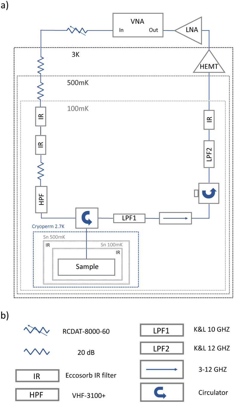
Experimental setup. (a) Schematic of the ADR thermal and radiation shielding, and (b) microwave components for reflectometry measurements. The resistor symbols represent thermalized attenuators. IR, HPF and LPF are infrared and high-pass and low-pass filters, respectively.
Microwave measurements
The performance of a CPW resonator can be characterized by the quality factor, which is a measure of how many oscillations the system needs to dissipate its energy. The internal quality factor is defined as the rate at which the energy is lost to parasitic effects of the environment which indicates how much the device is dissipative (high indicates less dissipation). The coupling quality factor is defined as the rate at which the energy stored in the resonator escapes into a larger component, and in our design indicates how strongly or weakly a resonator is capacitively coupled to the transmission line (fixed in the design ). The two quantities are related by the measured quality factor ().
Two-level systems (TLS) are a key source of loss in resonators, with their impact expected to reach a maximum at high power levels13. As a result, if a TLS channel significantly contribute to the total loss, the intrinsic quality factor () should rise with power up to a certain point. This behavior helps distinguish TLS-related loss channels from those caused by other mechanisms. The characteristic values can be determined by changing the power used to probe the resonator and plotting against the average photon number (). This relationship can be modeled as follows48:
| 1 |
where represents TLS loss at low power, (which is less than or equal to 1) is a scaling factor, is the critical photon number, and denotes other loss channels that are independent of power and to which ultimately saturates at high drive powers. In a strong field near a critical photon number , resonates and gets increasingly coupled to the microwave signal which induces an increase in at low power and temperature, resulting in a decrease of . For refection measurements, the average photon number is related to the input power as follows:
| 2 |
where is the average photon number in the resonator, is the drive microwave power and is the resonance frequency49. For CPW resonators, the electric fields vary along the CPW structure resulting in an effective value of for spatially uniform TLS distribution, while the value of in uniform structures50.
Acknowledgements
This work was funded by the U.S. Department of Energy, Office of Science, Office of Basic Energy Sciences, Materials Sciences and Engineering Division under Contract No. DE-AC02-05-CH11231 “High-Coherence Multilayer Superconducting Structures for Large Scale Qubit Integration and Photonic Transduction program (QIS-LBNL)”. We would like to thank Prof. Irfan Siddiqi for valuable discussions on the work. We also thank Ahmed Hajr for assistance with cryogenic setups. We would also like to acknowledge UC Berkeley Marvell Nanofabrication Laboratory, where device fabrication was primarily performed as well as Molecular Foundry at Lawrence Berkeley National Laboratory and Nanofabrication Core Labs at King Abdullah University of Science and Technology, where all materials analysis were performed.
Author contributions
All authors contributed equally to this work, with the project being led by MA and SR.
Data availibility
The datasets generated during and/or analysed during the current study are available from the corresponding author on reasonable request.
Declarations
Competing interests
The authors declare no competing interests.
Footnotes
Publisher’s note
Springer Nature remains neutral with regard to jurisdictional claims in published maps and institutional affiliations.
Contributor Information
Mohammed Alghadeer, Email: ghadeer@berkeley.edu, Email: mohammed.alghadeer@physics.ox.ac.uk.
Saleem Rao, Email: saleemg@kfupm.edu.sa.
References
- 1.Brecht, T. et al. Demonstration of superconducting micromachined cavities. Appl. Phys. Lett.107 (2015).
- 2.Place, A. P. et al. New material platform for superconducting transmon qubits with coherence times exceeding 0.3 milliseconds. Nat. Commun.12, 1779 (2021). [DOI] [PMC free article] [PubMed] [Google Scholar]
- 3.Vepsäläinen, A. et al. Improving qubit coherence using closed-loop feedback. Nat. Commun.13, 1932 (2022). [DOI] [PMC free article] [PubMed] [Google Scholar]
- 4.Blais, A., Huang, R.-S., Wallraff, A., Girvin, S. M. & Schoelkopf, R. J. Cavity quantum electrodynamics for superconducting electrical circuits: An architecture for quantum computation. Phys. Rev. A69, 062320 (2004). [Google Scholar]
- 5.Wallraff, A. et al. Strong coupling of a single photon to a superconducting qubit using circuit quantum electrodynamics. Nature431, 162–167 (2004). [DOI] [PubMed] [Google Scholar]
- 6.Mariantoni, M. et al. Implementing the quantum von neumann architecture with superconducting circuits. Science334, 61–65 (2011). [DOI] [PubMed] [Google Scholar]
- 7.Sillanpää, M. A., Park, J. I. & Simmonds, R. W. Coherent quantum state storage and transfer between two phase qubits via a resonant cavity. Nature449, 438–442 (2007). [DOI] [PubMed] [Google Scholar]
- 8.Hofheinz, M. et al. Synthesizing arbitrary quantum states in a superconducting resonator. Nature459, 546–549 (2009). [DOI] [PubMed] [Google Scholar]
- 9.Reagor, M. et al. Reaching 10 ms single photon lifetimes for superconducting aluminum cavities. Appl. Phys. Lett.102 (2013).
- 10.Martinis, J. M. et al. Decoherence in josephson qubits from dielectric loss. Phys. Rev. Lett.95, 210503 (2005). [DOI] [PubMed] [Google Scholar]
- 11.Müller, C., Cole, J. H. & Lisenfeld, J. Towards understanding two-level-systems in amorphous solids: insights from quantum circuits. Rep. Prog. Phys.82, 124501 (2019). [DOI] [PubMed] [Google Scholar]
- 12.Gao, J. et al. Experimental evidence for a surface distribution of two-level systems in superconducting lithographed microwave resonators. Appl. Phys. Lett.92 (2008).
- 13.McRae, C. R. H. et al. Materials loss measurements using superconducting microwave resonators. Rev. Sci. Instrum.91 (2020). [DOI] [PubMed]
- 14.Burnett, J., Faoro, L. & Lindström, T. Analysis of high quality superconducting resonators: consequences for tls properties in amorphous oxides. Supercond. Sci. Technol.29, 044008 (2016). [Google Scholar]
- 15.Woods, W. et al. Determining interface dielectric losses in superconducting coplanar-waveguide resonators. Phys. Rev. Appl.12, 014012 (2019). [Google Scholar]
- 16.Earnest, C. T. et al. Substrate surface engineering for high-quality silicon/aluminum superconducting resonators. Supercond. Sci. Technol.31, 125013 (2018). [Google Scholar]
- 17.McRae, C. R. H. et al. Dielectric loss extraction for superconducting microwave resonators. Appl. Phys. Lett. 116 (2020).
- 18.Murray, C. E. Material matters in superconducting qubits. Mater. Sci. Eng. R: Rep.146, 100646 (2021). [Google Scholar]
- 19.Gao, J. The physics of superconducting microwave resonators (California Institute of Technology, 2008).
- 20.Calusine, G. et al. Analysis and mitigation of interface losses in trenched superconducting coplanar waveguide resonators. Appl. Phys. Lett.112 (2018).
- 21.Lisenfeld, J. et al. Observation of directly interacting coherent two-level systems in an amorphous material. Nat. Commun.6, 6182 (2015). [DOI] [PMC free article] [PubMed] [Google Scholar]
- 22.Richardson, C. J. et al. Fabrication artifacts and parallel loss channels in metamorphic epitaxial aluminum superconducting resonators. Supercond. Sci. Technol.29, 064003 (2016). [Google Scholar]
- 23.Megrant, A. et al. Planar superconducting resonators with internal quality factors above one million. Appl. Phys. Lett.100 (2012).
- 24.Richardson, C., Alexander, A., Weddle, C., Arey, B. & Olszta, M. Low-loss superconducting titanium nitride grown using plasma-assisted molecular beam epitaxy. J. Appl. Phys.127 (2020).
- 25.Altoé, M. V. P. et al. Localization and mitigation of loss in niobium superconducting circuits. PRX Quant.3, 020312 (2022). [Google Scholar]
- 26.Ding, Z. et al. A stable and low loss oxide for superconducting qubits. arXiv preprint arXiv:2305.11395 (2023).
- 27.Zheng, K. et al. Nitrogen plasma passivated niobium resonators for superconducting quantum circuits. Appl. Phys. Lett.120, 13/14 (2022).
- 28.Bal, M. et al. Systematic improvements in transmon qubit coherence enabled by niobium surface encapsulation. arXiv preprint arXiv:2304.13257 (2023).
- 29.Alghadeer, M. et al. Surface passivation of niobium superconducting quantum circuits using self-assembled monolayers. ACS Appl. Mater. Interfaces15, 2319–2328 (2022). [DOI] [PubMed] [Google Scholar]
- 30.Love, J. C., Estroff, L. A., Kriebel, J. K., Nuzzo, R. G. & Whitesides, G. M. Self-assembled monolayers of thiolates on metals as a form of nanotechnology. Chem. Rev.105, 1103–1170 (2005). [DOI] [PubMed]
- 31.Onclin, S., Ravoo, B. J. & Reinhoudt, D. N. Engineering silicon oxide surfaces using self-assembled monolayers. Angewandte Chemie Int. Ed.44, 6282–6304 (2005). [DOI] [PubMed] [Google Scholar]
- 32.Chaki, N. K., Aslam, M., Sharma, J. & Vijayamohanan, K. Applications of self-assembled monolayers in materials chemistry. J. Chem. Sci.113, 659–670 (2001). [Google Scholar]
- 33.Casalini, S., Bortolotti, C. A., Leonardi, F. & Biscarini, F. Self-assembled monolayers in organic electronics. Chem. Soc. Rev.46, 40–71 (2017). [DOI] [PubMed] [Google Scholar]
- 34.Sushko, M. L. & Shluger, A. L. Rough and fine tuning of metal work function via chemisorbed self-assembled monolayers. Adv. Mater.21, 1111–1114 (2009). [Google Scholar]
- 35.Heitzer, H. M., Marks, T. J. & Ratner, M. A. Maximizing the dielectric response of molecular thin films via quantum chemical design. ACS Nano8, 12587–12600 (2014). [DOI] [PubMed] [Google Scholar]
- 36.Laibinis, P. E. & Whitesides, G. M. Self-assembled monolayers of n-alkanethiolates on copper are barrier films that protect the metal against oxidation by air. J. Am. Chem. Soc.114, 9022–9028 (1992). [Google Scholar]
- 37.Telegdi, J. Formation of self-assembled anticorrosion films on different metals. Materials13, 5089 (2020). [DOI] [PMC free article] [PubMed] [Google Scholar]
- 38.Goiri, E., Borghetti, P., El-Sayed, A., Ortega, J. E. & de Oteyza, D. G. Multi-component organic layers on metal substrates. Adv. Mater.28, 1340–1368 (2016). [DOI] [PubMed] [Google Scholar]
- 39.Rissner, F., Egger, D. A., Romaner, L., Heimel, G. & Zojer, E. The electronic structure of mixed self-assembled monolayers. ACS Nano4, 6735–6746 (2010). [DOI] [PMC free article] [PubMed] [Google Scholar]
- 40.Romaner, L., Heimel, G., Ambrosch-Draxl, C. & Zojer, E. The dielectric constant of self-assembled monolayers. Adv. Funct. Mater.18, 3999–4006 (2008). [Google Scholar]
- 41.Van Dyck, C., Marks, T. J. & Ratner, M. A. Chain length dependence of the dielectric constant and polarizability in conjugated organic thin films. ACS Nano11, 5970–5981 (2017). [DOI] [PubMed] [Google Scholar]
- 42.Chen, X. & Nijhuis, C. A. The unusual dielectric response of large area molecular tunnel junctions probed with impedance spectroscopy. Adv. Electron. Mater.8, 2100495 (2022). [Google Scholar]
- 43.Ebensperger, N. G. et al. Characterizing dielectric properties of ultra-thin films using superconducting coplanar microwave resonators. Rev. Sci. Instrum.90 (2019). [DOI] [PubMed]
- 44.Akkerman, H. B., Blom, P. W., De Leeuw, D. M. & De Boer, B. Towards molecular electronics with large-area molecular junctions. Nature441, 69–72 (2006). [DOI] [PubMed] [Google Scholar]
- 45.Liu, Y., Qiu, X., Soni, S. & Chiechi, R. C. Charge transport through molecular ensembles: Recent progress in molecular electronics. Chem. Phys. Rev.2 (2021).
- 46.Rao, S. G., Huang, L., Setyawan, W. & Hong, S. Large-scale assembly of carbon nanotubes. Nature425, 36–37 (2003). [DOI] [PubMed] [Google Scholar]
- 47.Oh, J.-S. et al. Structure and formation mechanisms in tantalum and niobium oxides in superconducting quantum circuits. ACS Nano18, 19732–19741 (2024). [DOI] [PMC free article] [PubMed] [Google Scholar]
- 48.Pappas, D. P., Vissers, M. R., Wisbey, D. S., Kline, J. S. & Gao, J. Two level system loss in superconducting microwave resonators. IEEE Trans. Appl. Supercond.21, 871–874 (2011). [Google Scholar]
- 49.Bruno, A. et al. Reducing intrinsic loss in superconducting resonators by surface treatment and deep etching of silicon substrates. Appl. Phys. Lett. 106 (2015).
- 50.Khalil, M. S., Wellstood, F. & Osborn, K. D. Loss dependence on geometry and applied power in superconducting coplanar resonators. IEEE Trans. Appl. Supercond.21, 879–882 (2010). [Google Scholar]
Associated Data
This section collects any data citations, data availability statements, or supplementary materials included in this article.
Data Availability Statement
The datasets generated during and/or analysed during the current study are available from the corresponding author on reasonable request.