

Abstract
In this work, ZnO nanoparticles (NPs) are synthesized using avocado seed extract and annealed at different annealing temperatures from 400 to 800 °C. The morphology of the nanoparticles changes from poly shapes at 400 °C to spherical ones at 800 °C, and particle sizes increase from ∼42 nm to ∼128 nm. The Ag/ZnO@400/FTO memory device exhibits stable resistive switching over 100 cycles and a resistance window of approximately 150. Also, the performance characteristics of ZnO@600 and ZnO@800-based devices are degraded gradually over operating cycles. The concentration of oxygen interstitials (Oi) in ZnO nanoparticles, which may originate from organic residues, decreases as the annealing temperature increases. These Oi ions reduced the energy barrier at the interfaces, facilitating electron transport under an external electric field. This study has demonstrated the close correlation between resistive switching characteristics and organic residuals in green synthesized nanoparticles.
The analog characteristics and RS mechanism of ZnO-based memristors.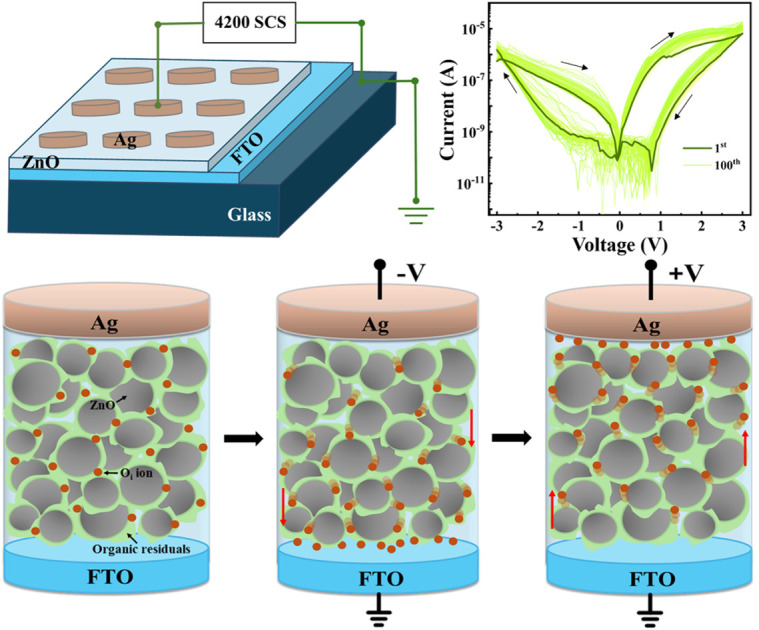
1. Introduction
In recent years, research into the synthesis and application of nanomaterials has emerged as a promising field in technology and science. Zinc oxide nanoparticles (ZnO NPs) are a promising nanomaterial due to their stability, large bandgap (3.37 eV), photocatalytic properties, and high biocompatibility.1 Traditional ZnO NP synthesis methods, on the other hand, are frequently associated with expensive equipment, high energy consumption, significant costs, and potential environmental and health risks.2 With the goal of sustainable development and the creation of high-performance materials, green synthesis has become a preferred choice among methods for producing ZnO NPs.3
Green synthesis produces nanomaterials using biologically derived reducing agents such as microorganisms, algae, and plant extracts, which have several advantages, including environmental friendliness, simplicity, and low energy consumption.4 Plant-based synthesis of ZnO NPs offers advantages over microbial or algal-based methods, such as abundant raw materials, shorter reaction times, fewer purification steps, and simpler processes, all while remaining environmentally friendly.5,6 Green synthesis can yield ZnO NPs of various shapes and sizes by adjusting parameters such as pH, precursor concentrations, and annealing temperatures.7 Among them, the annealing temperature has a significant impact on the morphology and size of nanoparticles. For example, S. Azizi et al. demonstrated that increasing the calcination temperature from 100 °C to 200 °C resulted in uniform, hexagonal ZnO NPs with sizes ranging from 10 to 18 nm, while lower temperatures produced poorly crystalline particles.8 Similarly, N. Sedefoglu et al. investigated the effect of raising the calcination temperature from 400 to 800 °C, which transformed ZnO NPs from spherical to hexagonal rods, with an average size of about 100 nm.9
ZnO NPs have been extensively researched for their resistive switching properties, which are essential for the development of resistive random-access memory (RRAM) devices, as well as for a variety of other applications, such as food packaging,10 antimicrobial materials,11 and optoelectronic devices.12 The resistive switching behavior of ZnO NPs is particularly significant in the development of RRAM technology, as it enables high-speed data storage, energy efficiency, and scalability. ZnO NPs are anticipated to be a significant component of next-generation data storage solutions, as the demand for more efficient memory devices increases. They provide faster retrieval times and larger capacities than conventional systems, such as static random-access memory (SRAM). This transition is aided by several benefits, including ease of fabrication, high scalability, simple architecture, high integration density, and rapid switching.13 Furthermore, their simple architecture and compatibility with green synthesis methods make them ideal candidates for sustainable electronics manufacturing.
While green synthesis offers an eco-friendly approach, the specific impact of organic residuals on device performance is not fully understood. Our research, for example, investigates the effect of annealing temperature on ZnO properties through green synthesis and their application in analog memristors.14 However, further study should be conducted to fully understand how these organic residuals affect the electrical properties and overall performance of the device. However, beyond these intrinsic factors, external influences, such as light, can also modulate the electronic properties of ZnO. Garcia et al. have highlighted that light-induced effects can significantly enhance the photoconductivity and nonlinear optical behavior of ZnO material, creating further potential for applications in data storage and optoelectronic devices.15 Investigating these light-induced effects could further enhance the applicability of ZnO in data storage devices, particularly in environments where photoresponse is critical, potentially improving the performance of memory devices and optoelectronic systems.
In this study, we explore the impact of annealing temperature on the morphological and structural properties of ZnO NPs synthesized via a green method using avocado seed extract. Particularly, the study investigates the effect of organic precursor residuals within ZnO NPs on the resistive switching behavior of memory devices, providing a thorough analysis of the underlying mechanisms. This study expands our understanding of ZnO NPs' applications and the influence of the green synthesis process.
2. Experimental procedures
2.1. Materials
Zinc nitrate hexahydrate [Zn(NO3)2·6H2O] was sourced from Sigma-Aldrich, USA. Additionally, commercial ZnO nanoparticles were provided by Merck. An S60H Elmasonic bath from Elma, Germany, was utilized for ultrasonic cleaning in the processes of synthesis and dispersion before dip coating. Ripe avocado seeds were collected from various avocado outlets in Ho Chi Minh City, Vietnam.
2.2. The ZnO NPs synthesis and RRAM device fabrication
Initially, ZnO NPs were synthesized through a green chemistry approach using avocado seed extract. The avocado seeds were washed, dried, and ground into powder. Then, 20 g of avocado seed powder was added to a glass vessel containing 100 mL of deionized (DI) water and stirred continuously at 80 °C for 60 minutes using a magnetic stirrer. The resulting extract was filtered using Whatman filter paper and stored at 4 °C.
For the synthesis, 14.875 g of Zn(NO3)2·6H2O was dissolved in 100 mL of DI water to prepare a 0.5 M Zn(NO3)2 solution. A total of 40 mL of this solution was then slowly added dropwise to a vessel containing 10 mL of avocado seed extract, and the mixture was stirred continuously at 50 °C for 2 hours. The resulting blend was dried at 150 °C for 2 hours to obtain dry samples. These dried samples were then calcined at 400 °C, 600 °C, and 800 °C for 2 hours each to study the effect of temperature on the nanoparticle properties.
Next, the ZnO NPs treated at different calcination temperatures are dispersed in DI water at a concentration of 1wt%. Concurrently, fluorine-doped tin oxide (FTO) substrates are thoroughly cleaned and dried. The FTO substrates are immersed directly in a glass beaker containing the ZnO NP suspension for film deposition. Each immersion step lasts 10 minutes, followed by 5 minutes of drying before the next immersion. The coating procedure is repeated four times to ensure uniform coverage. Finally, the Ag top electrode is sputter-deposited to complete the Ag/ZnO/FTO device assembly. For convenience, ZnO was synthesized at 400 °C, 600 °C, and 800 °C, denoted as ZnO@400, ZnO@600, and ZnO@800, respectively. To compare, devices using commercial ZnO NPs were fabricated following a similar procedure. This synthesis process of ZnO NPs and memristors is depicted in Fig. 1.
Fig. 1. Schematic process of FTO/ZnO/Ag device fabrication using ZnO NPs.

2.3. Material and device characterization
In this study, ZnO NPs were synthesized and analyzed using analytical techniques to investigate their structural, morphological, and optical characteristics. X-ray diffraction (XRD) was performed on a D8-Bruker system utilizing CuKα radiation (λ = 1.54060 Å) across a scan range of 20–80° (2θ).
The particle size (D) was determined by the Debye–Scherer equation below:16
 |
1 |
where D represents particle size, K is the shape factor, λ is the X-ray wavelength, β is the full width at half maximum (FWHM) of the peak in radians, and θ is the Bragg angle, was employed to deduce the nanoparticles' size.
Fourier-transform infrared (FTIR) spectroscopy, performed on a Bruker TENSOR 27 instrument within the 400–4000 cm−1 range, identified the functional groups and chemical bonds in the ZnO NPs, revealing insights into their chemical composition. The Horiba XploRa Plus Raman scattering spectrometer with a 532 nm excitation source supplemented the FTIR results by providing detailed information on the vibrational modes associated with ZnO's crystalline structure.
The morphology and size of the nanoparticles were characterized using scanning electron microscope (SEM) images captured with a Hitachi S4800 (Japan). The elemental composition and purity were assessed using Energy-Dispersive X-ray Spectroscopy (EDX) on the JEOL JSM-IT200 system. Thermogravimetric Analysis (TGA) was used to determine the thermal stability and composition of the ZnO nanoparticles. The TGA was carried out in a nitrogen atmosphere at room temperature and up to 800 °C. The weight loss curves obtained from TGA revealed the thermal degradation pattern and confirmed the removal of organic residues and water molecules adsorbed on the nanoparticles' surfaces.
Diffuse Reflectance Spectroscopy (DRS) was used to evaluate the optical properties with a Jasco V770 system, covering a wavelength range of 200 nm to 800 nm and providing an initial assessment of the ZnO nanoparticles' absorption capabilities. The optical band gap of ZnO NPs was calculated using the Kubelka–Munk equation:
 |
2 |
above, R is the percent reflectance, K is the absorbance coefficient, and S is the scattering coefficient. The absorption coefficient α is given by αhv = A(hv − Eg)γ, where hv is the photon energy, A is the proportionality constant and Eg is the band gap.17 The exponent γ in the Tauc plot depends on the electronic transition: γ = 2 for allowed indirect, γ = 1/2 for allowed direct, γ = 3 for forbidden indirect, and γ = 3/2 for forbidden direct transitions. Since ZnO is a direct band gap semiconductor, γ is set to 1/2.18 Additionally, photoluminescence (PL) spectroscopy was performed with a Horiba iHR550 instrument and a 355 nm excitation source to analyze the energy-band structure of the material, with a particular emphasis on crystal defects. X-ray photoelectron spectroscopy (XPS, Thermo K-Alpha) using an Al-Kα radiation source (1486.6 eV) was also employed to examine the binding states of elements in the samples.
In voltage sweep mode, the devices' resistive switching (RS) performance was evaluated using a Keithley 4200-SCS parameter analyzer. During the assessment, the voltage was cycled from 0 to −Vmax and back, then from 0 to +Vmax and returned to 0. The alternating cycle was repeated several times to assess the stability of the RRAM devices.
3. Results and discussion
Fig. 2 depicts the morphology and particle size distribution of ZnO nanoparticles synthesized using a green synthesis and annealed at various temperatures. Fig. 2(a) exhibits the morphology of the ZnO sample annealed at 400 °C, revealing various forms and a tendency to form larger clusters. Fig. 2(b) shows that when the annealing temperature reaches 600 °C, the ZnO NPs primarily form hexagonal and spherical shapes. At 800 °C, ZnO changes significantly in shape and size. These particles are discrete, with primarily spherical and tubular shapes, as shown in Fig. 2(c). ZnO@400 sample has an average particle size of 42 nm, with a range of 15 to 90 nm, as shown in Fig. 2(d). The average particle size of the ZnO@600 sample increases to around 77.5 nm, with a range of 44 to 115 nm (Fig. 2(e)). Fig. 2(f) shows that at 800 °C, the average particle size increases to approximately 128 nm, with a range of 75 to 180 nm. SEM analysis confirms that as the calcination temperature rises, the size of the ZnO NPs gradually increases, consistent with previous studies on the effects of annealing temperatures on ZnO. These morphological and particle size changes are attributed to crystal growth and the reduction of residual organic at elevated temperatures.19,20 Additionally, commercial ZnO NPs (ZnO@CM) were used as a control, exhibiting cylindrical round morphologies with an average size of approximately 206.6 nm, ranging from 130 to 280 nm, as shown in Fig. S1 (ESI).†
Fig. 2. The SEM images and size distribution of ZnO NPs at various calcination temperatures: 400 °C (a, and d), 600 °C (b, and e), 800 °C (c, and f).

The Raman scattering spectroscopy was used to analyze lattice vibrations in ZnO samples calcined at 400, 600, and 800 °C, as shown in Fig. 3(a). The spectra of all samples show prominent first-order phonon modes, specifically E2L at approximately 74 cm−1 and E2H at around 431 cm−1, which represent the vibrations of the Zn and O atoms, respectively.21 In addition, a mode at 372 cm−1 corresponding to the A1(TO) was detected, which was associated with lattice defects. The presence of phonon states such as A1(LO)/E1(LO) at approximately 578 cm−1 commonly signifies surface defects like zinc and oxygen vacancies in the ZnO lattice.22 The detection of second-order and multi-phonon modes such as 2E2L, E2H–2L22 and 2LA23 confirms ZnO's wurtzite structure. However, the E2L peak shifted to higher frequencies (90 cm−1 for ZnO@600 and 93 cm−1 for ZnO@800). The E2H mode remains intense in these samples, indicating the high crystallinity and purity of the ZnO lattice.24
Fig. 3. (a) Raman spectroscopy, (b) XRD pattern, (c) the FTIR spectra, (d) EDX, (e) DRS and Tauc plot, (f) TGA of ZnO NPs synthesized at various calcination temperatures.

The X-ray diffraction patterns of ZnO NPs treated at various temperatures are shown in Fig. 3(b). The ZnO@400 exhibited preferred diffraction peaks at 2θ angles of 31.82°, 36.32°, and 34.49°, representing the (100), (002), and (101) planes, respectively. The other diffraction peaks at 47.60°, 56.67°, 62.91°, 68.018°, 69.17°, and 77.04° correspond to the (102), (110), (103), (112), (201), and (202) planes. These plane orientations are consistent with the standard XRD pattern (JSPDS_36-1451) for a wurtzite structure, which matches the Raman spectroscopy results. When the calcination temperature was increased to 600 °C and 800 °C, there were no significant changes in the diffraction peaks compared to the sample calcined at 400 °C. The most noticeable peak, corresponding to the plane (101), preferred growth direction. The average crystal size of ZnO NPs, calculated from the (101) plane, increased slightly with treated temperature, measuring 36.2 nm, 38.9 nm, and 41.4 nm for ZnO@400, ZnO@600, and ZnO@800, respectively. This increment is because, at higher temperatures, atoms have more energy to move and stabilize at optimal positions within the crystal lattice. Consequently, grains with lower surface energy become more prominent as the calcination temperature increases.25 The crystalline characteristic of commercial ZnO NPs is similar to synthesized nanoparticles, as shown in Fig. S2.†
The FTIR spectra, shown in Fig. 3(c), reveal characteristic bands of several functional groups in all samples annealed at 400, 600, and 800 °C. The FTIR results for ZnO@400 show a broad peak from 3170 to 3650 cm−1, indicating the stretching vibrations of the O–H bond on the surface of ZnO NPs. The broadband from 1120 to 1554 cm−1, with the highest peak at 1373 cm−1 is attributed to overlapping vibrations from various functional groups, such as the C C in amide groups, the stretching deformation of the C–O group, and the phenolic O–H group.26 Additionally, a peak at 1608 cm−1 with weaker intensity corresponds to the stretching vibrations of the C O group.27 The FTIR spectra of ZnO@600 and ZnO@800 show similar vibrations but with lower intensities of the organic groups, indicating that organic residues gradually decrease as the calcination temperature rises. Notably, ZnO@400 exhibits broad, strong absorption peaks at 474 cm−1, indicative of the Zn–O bond.28 This absorption peak shifts slightly to higher wavenumbers at 476 and 477 cm−1 in ZnO@600 and ZnO@800, respectively. This minor shift in the Zn–O peak is attributed to changes in particle size and induced strain resulting from the varying calcination temperatures.29 The FTIR spectrum of commercial ZnO indicates a prominent broad peak with high intensity at 420 cm−1 and no peaks or bands associated with impurities, confirming the purity of nanoparticles depicted in Fig. S2(b).†
Fig. 3(d) shows the EDX spectra of ZnO NPs, which contain significant amounts of Zn, O, and C. Elemental analysis reveals that the carbon content decreases from 21.9 to 8.06 at% as the annealing temperature rises from 400 to 800 °C. This result is consistent with FTIR analysis, which indicated a reduction in organic moieties with increasing annealing temperature. Fig. 3(e) depicts the mass loss of ZnO NPs when heated to various temperatures. For ZnO@400, the weight loss occurring up to 500 °C is primarily due to moisture and –OH groups on the ZnO surface; from 500 °C to 800 °C, a significant mass reduction is observed caused by the decomposition of remaining organic residues within the ZnO NPs. In contrast, ZnO@600 shows no considerable mass loss from 100 °C to 600 °C compared to ZnO@400, which can be attributed to a gradual reduction of –OH bonds and organic groups, as demonstrated by FTIR analysis. The primary weight loss occurs as the temperature rises to 600 °C, resulting from the decomposition of more stable, difficult-to-decompose organic compounds. Meanwhile, for ZnO@800, the mass loss is primarily caused by the degradation of residual –OH and –C–O bonds formed during synthesis. Fig. 3(f) shows DRS studies on ZnO NPs at various temperatures. The spectra show a prominent peak that decreases from 385 nm to 373 nm as the annealing temperature rises from 400 °C to 800 °C. The band gap of ZnO NPs was calculated from the Tauc plot derived from Kubelka–Munk transformed absorbance data. The results show that the band gap values for ZnO gradually increase from 3.17 eV to 3.22 eV as the temperature rises from 400 °C to 800 °C. This band gap energy increase is attributed to particle size enlargement with rising calcination temperatures.28 The transmission and band gap of 3.26 eV for commercial ZnO is shown in Fig. S2(c and d).†
ZnO, with its tunable electrical properties, wide band gap, and several advantages such as low cost, abundance, non-toxicity, and ease of synthesis, is a highly promising material for RRAM applications.30 Its flexibility in synthesis allows for different doping and structural modifications, making it adaptable for various resistive switching applications. Furthermore, its compatibility with environmentally friendly, green synthesis methods makes ZnO an appealing option for sustainable electronics. However, challenges such as particle size control must be addressed in order to ensure consistent device performance. To further investigate its potential in RRAM, devices with various ZnO annealing temperatures were created. These include Ag/ZnO@400/FTO (M1), Ag/ZnO@600/FTO (M2), and Ag/ZnO@800/FTO (M3). ZnO NPs were annealed at 400 °C, 600 °C, and 800 °C. For comparison, a device with commercial ZnO, Ag/ZnO@CM/FTO (M4), was also fabricated. The current–voltage (I–V) characteristics of all devices are presented in Fig. 4.
Fig. 4. Current–voltage (I–V) characteristic curves for (a) Ag/ZnO@400/FTO (M1), (b) Ag/ZnO@600/FTO (M2), (c) Ag/ZnO@800/FTO (M3) and (d) Ag/ZnO@CM/FTO (M4) devices with subpanels: (1) displaying a linear scale, (2) presenting a semi-log scale, (3) depicting the endurance test of the RRAM device, and (4) illustrating the derived ON/OFF ratio.

The resistive switching behavior was clearly evident within the voltage range of −3 to 3 V, as shown in Fig. 4(a1). During negative polarization, the device switched from the high resistance (HRS) to the low resistance (LRS) state, corresponding to the SET process. In contrast, the RESET process occurred during positive polarization when the voltage was applied from 0 to 3 V, as shown in Fig. 4(a2). Durability tests confirmed that the M1 device was stable for up to 100 continuous cycles, as illustrated in Fig. 4(a3). The on/off ratio had reached approximately 400 at a reading voltage of 1.5 V, with HRS and LRS values remaining stable, ranging from 1.1 × 10⁻⁹ to 1.05 × 10⁻⁹ A for HRS and 5.6 × 10⁻⁷ to 2.4 × 10⁻⁶ A for LRS, as depicted in Fig. 4(a4). In R. Deb et al.'s study, incorporating ZnO NPs significantly enhanced the memory window to approximately 103, compared to around 102 in devices without ZnO.31 Their devices also showed high durability, maintaining stability over roughly 103 cycles. While both studies report stable switching performance, Deb et al.'s devices had a higher on/off ratio and durability, likely due to their specific material composition and structure.31 A key difference is their use of nanocomposites, combining ZnO NPs with a polymer matrix, which improved charge trapping mechanisms and stabilized the resistive switching behavior.32 This resulted in a broader memory window and enhanced durability in digital memory devices, whereas our study focuses on analog memristors.
The I–V characteristic of the M2 device, depicted in Fig. 4(b2), displayed a behavior similar to the M1 device. The SET process occurred at negative biases, while the RESET process was observed at positive biases. However, the switching effect was observed within a narrower voltage range of −1.5 to 1.5 V and tended to narrow as the number of cycles increased. The M2 device's I–V characteristic was repeatable for 60 cycles and tended to narrow as the number of cycles increased, as shown in Fig. 4(b3). Additionally, the resistance distribution analysis showed significant fluctuations in the values of the HRS and LRS under a small reading voltage of 0.5 V during the final cycles, as shown in Fig. 4(b4). The LRS values varied from 4.8 × 10⁻⁷ to 8.4 × 10⁻⁶ A, while the HRS values ranged from 1.8 × 10⁻⁸ to 1.0 × 10⁻⁵ A.
The I–V characteristics of the device utilizing ZnO@800 were scrutinized, with the findings depicted in Fig. 4(c). The resistive switching process was evident within a voltage range of −3.5 to 3.5 V. The SET and RESET processes were observed at negative and positive polarities, respectively. Furthermore, the I–V curve showed significant noise, as shown in Fig. 4(c2). The device exhibited limited stability, enduring around 50 cycles, as evidenced in Fig. 4(c3). Similar to the M2 device, the resistance window of the ZnO@800 narrows during the final cycles. The distribution of HRS values at 1.5 V fluctuated significantly, ranging from 2.8 × 10⁻¹⁰ to 4.5 × 10⁻⁸ A, while the LRS values varied between 1.3 × 10⁻⁷ and 6.8 × 10⁻⁷ A, indicating instability in both states, as shown in Fig. 4(c4).
Fig. 4(d) depicts the I–V characteristics of the device utilizing commercial ZnO (M4). The SET and RESET processes occur sequentially at positive and negative polarities (Fig. 4(d2)). Furthermore, when investigating the device's durability, the results show instability after only about 15 cycles, as shown in Fig. 4(d3). The results depicted in Fig. 4(d4) show that the LRS and HRS have higher values compared to other devices, respectively ranging from 8.8 × 10⁻⁶ to 6.5 × 10⁻⁵A and 3.1 × 10⁻⁷ to 2.7 × 10⁻⁵A.
The characteristics of various ZnO-based devices reveal apparent differences in operating voltage, stability, and the resistance window, as described above. The M1 device demonstrates high stability with up to 100 voltage sweeps and an on/off ratio 150. In contrast, the M2 and M3 devices exhibit poorer stability, and their resistance windows tend to narrow with increasing scanning cycles. Memory devices using commercial ZnO exhibit several switching cycles with low stability. No significant structural differences among ZnO samples were confirmed by XRD and Raman. Meanwhile, FTIR and EDX show that organic residuals decrease as calcination temperature increases. These findings suggest that changes in device performance may be primarily caused by residual organic, which affects the device's electronic properties and stability. PL analyses in the following will clarify how these residuals impact the device's resistive switching behavior.
Fig. 5 shows the photoluminescence (PL) and X-ray photoelectron (XPS) results of the ZnO samples. All the PL spectra exhibit two central emission regions, including a near-band-edge (NBE) region located around 400 nm and deep-level emissions (DLE) ranging within intervals of 500–800 nm (Fig. 5(a)). The NBE region contains two emissions; the E1 at ∼390 nm is attributed to free-exciton (FX) emission,33 while the E2 at ∼402 nm originates from zinc interstitial (Zni)-related defects as shallow levels located at ∼0.2–0.5 eV below conduction band minimum (CBM).34 The DLE region is more complex, which is resolved into four component emissions for all the samples (Fig. 5(b–d)). The E3 (∼550 nm) and E4 (∼600 nm) can be related to singly-ionized oxygen vacancy (VO+) donor level35 and doubly-ionized oxygen vacancy (VO2+) acceptor level.36 The E5 can be assigned to the oxygen interstitial (Oi) acceptor level, whereas the electronic transition between Zni and Oi defect levels is responsible for the E6 emission.14,37
Fig. 5. Photoluminescence and X-ray photoelectron analyses of ZnO samples: (a) PL spectra attaching with possible electronic transition diagram, and Gaussian-deconvoluted spectra of (b) ZnO@400, (c) ZnO@600, and (d) ZnO@800 samples. (e) XPS survey spectra and (f) deconvoluted O 1s core-level spectra of the samples. The pie charts depict the contribution of resolved components to the total spectrum.

The inset pie charts depict the integrated intensity ratios of component emissions to the total spectrum, indicating the relative ratios of point defects in the samples. The intensity of E1 (FX) emission remarkably increases, suggesting the improvement in crystallinity of the ZnO samples with increasing annealing temperature. Despite the fluctuation in the E3 and E4 emissions, the total ratios of the VO-related defects tend to be unchangeable upon elevating the annealing temperature. Thus, the contribution of VO defects to the carrier transport of memristor structures can be similar among different ZnO layers. On the other hand, the total ratios of the Oi-related defects (E5 and E6) significantly decrease with increasing annealing temperature. It is noted that the Oi defects existing mainly in the residuals can act as ion reservoirs between ZnO particles through organic bridges. To confirm it, the PL analysis of commercial inorganic ZnO sample is considered in Fig. S3, and ESI.† Excepting the characteristic E1 and E2 peaks, no O-related emission is observed, indicating the absence of organic bridges in the commercial ZnO. Therefore, the reduction in Oi defects suggests a decrease in ion sources leading to a degradation in the memristor performance of ZnO-based structures upon increasing annealing temperature. The defect characteristics from PL analysis are more valuable if combined with quantum yield measurements. However, we regret the lack of this system, which will be seriously considered in future works.
Similarly, the XPS analysis was also conducted for all the samples (Fig. 5(e)). All the spectra record the binding states relating to Zn and O elements which are aligned with the C 1s state (284.8 eV).38 To support the variation in the Oi ratio of the samples, the O 1s core states are considered and deconvoluted using mixed Gaussian–Lorentzian function and Shirley baseline (Fig. 5(f)). The O 1s states include two sub-peaks attributed to O2− ions at O–Zn lattice points (O1, 531.7 ± 0.1 eV)39 and in O–C bonds (O2, 533.1 ± 0.2 eV) of residual organic components.40 The inset pie charts illustrate the integrated intensity ratios of the O1 and O2 components to the total spectrum. The O1 component increases while the O2 portion decreases with increasing annealing temperature. It suggests a better stoichiometric ZnO structure and a reduction in residual organic components upon elevating annealing temperature. This result well agrees with the above PL analysis, indicating the significant reduction in the organic bridges (or the Oi component) of the samples treated at high temperature.
The concentration of oxygen vacancies is relatively similar in ZnO NPs treated at 400–800 °C, whereas the oxygen interstitials (Oi) are quite different, as confirmed by PL analysis. In this study, the presence of oxygen interstitials within organic residuals significantly impacts the charge transport mechanism in memory devices based on ZnO NPs. These ions play a crucial role in the modulation of the energy barrier via accumulation at the interfaces (Fig. 6). When a negative bias voltage is applied to the top electrode, these Oi ions move to the counter electrode and accumulate at the ZnO/FTO interfaces. This movement may lead to a gradual reduction in the energy barrier at the interfaces, facilitating easier electron transport. As a result, the current increases, and the device switches to LRS. As the bias voltage is reversed, these Oi ions drift back to the top electrode, leading to the recovery of the energy barrier at ZnO/FTO, then the device switches to HRS. For Ag/ZnO@400/FTO devices, the high concentration of Oi ions, which are confirmed by PL and XPS analyses above, significantly reduces the energy barrier at the interfaces, thereby attributing to the reliable resistive switching characteristics. For the Ag/ZnO@600/FTO and Ag/ZnO@800/FTO devices, the critical reduction of Oi concentration makes them less effective in the energy barrier modulation, and the charge transfer is more challenging. Therefore, the performance of these devices gradually degrades with low endurance. These findings align with the results of Zhang et al., where Oi was also identified as a crucial factor in enhancing resistive switching (RS) behavior. Their study demonstrated that post-synthetic treatments, such as oxygen plasma treatment, increased the concentration of oxygen-related defects, including Oi, which improved RS characteristics by facilitating the formation and rupture of conductive pathways. Zhang et al. further showed that controlling Oi and oxygen vacancies through post-synthetic treatments or annealing conditions could optimize the balance between electrical conductivity and resistive switching performance.41
Fig. 6. The schematic of resistive switching mechanism in Ag/ZnO@400/FTO device.

4. Conclusion
In this study, ZnO NPs were synthesized using a friendly route and played as an insulator layer in resistive memory devices. FTIR and TGA confirmed the gradual decrease in the progressive decomposition of organic residues at higher annealing temperatures. Furthermore, our investigations revealed that the Ag/ZnO@400/FTO device exhibited high durability and stability, significantly outperforming the Ag/ZnO@600/FTO and Ag/ZnO@800/FTO devices. We elucidated the significant impact of organic residues on point defects, which may contribute to the modulation of the energy barrier at the interfaces and enhance the performance of the memory devices. This finding underscores the importance of organic residues in boosting the efficiency of nanoparticle-based memory devices synthesized using green methods.
Data availability
The data supporting this study's findings are available from the corresponding authors upon reasonable request.
Author contribution
Trung Bao Ngoc Duong: formal Analysis (lead), investigation (lead), writing draft (lead). Phu-Quan Pham: investigation (equal), formal analysis (lead). Anh Thuy Tran: data curation (supporting). Dat Tan Bui: formal analysis (supporting). Anh Tuan Thanh Pham: investigation (equal), writing draft (supporting). Tien Cam Thi Nguyen: formal analysis (equal). Linh Ho Thuy Nguyen: data curation (supporting). Thuy Dieu Thi Ung: data curation (supporting). Nam Vu Hoang: resource (lead), writing – review & editing (equal). Ngoc Kim Pham: supporting (lead), writing – review & editing (lead).
Conflicts of interest
The authors have no conflicts to disclose. The XRD, FTIR, Raman, XPS and EDX data of the ZnO@400 sample were reprinted with permission from ref. 40.
Supplementary Material
Acknowledgments
This research was supported by the University of Science, Vietnam National University, under grant number T2023-61.
Electronic supplementary information (ESI) available. See DOI: https://doi.org/10.1039/d4ra04381b
References
- Ifijen I. Maliki M. Anegbe B. Synthesis, Photocatalytic Degradation and Antibacterial Properties of Selenium or Silver Doped Zinc Oxide Nanoparticles: A Detailed Review. OpenNano. 2022;8:100082. doi: 10.1016/j.onano.2022.100082. doi: 10.1016/j.onano.2022.100082. [DOI] [Google Scholar]
- Hussain R. T. Hossain M. S. Shariffuddin J. H. Green synthesis and photocatalytic insights: A review of zinc oxide nanoparticles in wastewater treatment. Mater. Today Sustain. 2024;26:100764. doi: 10.1016/j.mtsust.2024.100764. [DOI] [Google Scholar]
- Agarwal H. Venkat Kumar S. Rajeshkumar S. A review on green synthesis of zinc oxide nanoparticles – An eco-friendly approach. Resour.-Effic. Technol. 2017;3:406–413. doi: 10.1016/j.reffit.2017.03.002. [DOI] [Google Scholar]
- Mishra S. Sahoo S. Sahoo P. K. Sahoo N. K. Recent advancements in the plant and microbial assisted green synthesis of nanomaterials. Mater. Today: Proc. 2023 doi: 10.1016/j.matpr.2023.10.144. [DOI] [Google Scholar]
- Vaseghi Z. Nematollahzadeh A. Tavakoli O. Green methods for the synthesis of metal nanoparticles using biogenic reducing agents: a review. Rev. Chem. Eng. 2018;34(4):529–559. doi: 10.1515/revce-2017-0005. doi: 10.1515/revce-2017-0005. [DOI] [Google Scholar]
- Pal G., Rai P., and Pandey A., Chapter 1 – Green synthesis of nanoparticles: A greener approach for a cleaner future, in Green Synthesis, Characterization and Applications of Nanoparticles, ed. A. K. Shukla, and S. Iravani, Elsevier, 2019, pp. 1–26, 10.1016/B978-0-08-102579-6.00001-0 [DOI] [Google Scholar]
- Shaba E. Y. Jacob J. O. Tijani J. O. Suleiman M. A. T. A critical review of synthesis parameters affecting the properties of zinc oxide nanoparticle and its application in wastewater treatment. Appl. Water Sci. 2021;11:48. doi: 10.1007/s13201-021-01370-z. doi: 10.1007/s13201-021-01370-z. [DOI] [Google Scholar]
- Azizi S. Mohamad R. Bahadoran A. Bayat S. Rahim R. A. Ariff A. Saad W. Z. Effect of annealing temperature on antimicrobial and structural properties of bio-synthesized zinc oxide nanoparticles using flower extract of Anchusa italica. J. Photochem. Photobiol., B. 2016;161:441–449. doi: 10.1016/j.jphotobiol.2016.06.007. doi: 10.1016/j.jphotobiol.2016.06.007. [DOI] [PubMed] [Google Scholar]
- Sedefoglu N. Green synthesis of ZnO nanoparticles by Myrtus communis plant extract with investigation of effect of precursor, calcination temperature and study of photocatalytic performance. Ceram. Int. 2024;50:9884–9895. doi: 10.1016/j.ceramint.2024.01.387. doi: 10.1016/j.ceramint.2024.01.387. [DOI] [Google Scholar]
- Espitia P. J. P., Otoni C. G., and Soares N. F. F., Chapter 34 – Zinc Oxide Nanoparticles for Food Packaging Applications, in Antimicrobial Food Packaging, ed. J. Barros-Velázquez, Academic Press, San Diego, 2016, pp. 425–431, 10.1016/B978-0-12-800723-5.00034-6 [DOI] [Google Scholar]
- Gudkov S. V. Burmistrov D. E. Serov D. A. Rebezov M. B. Semenova A. A. Lisitsyn A. B. A Mini Review of Antibacterial Properties of ZnO Nanoparticles. Front. Phys. 2021;9:641481. doi: 10.3389/fphy.2021.641481. doi: 10.3389/fphy.2021.641481. [DOI] [Google Scholar]
- Qiao F. Sun K. Chu H. Wang J. Xie Y. Chen L. Yan T. Design strategies of ZnO heterojunction arrays towards effective photovoltaic applications. Battery Energy. 2022;1:20210008. doi: 10.1002/bte2.20210008. doi: 10.1002/bte2.20210008. [DOI] [Google Scholar]
- Banerjee W. Liu Q. Long S. Lv H. Liu M. Crystal that remembers: several ways to utilize nanocrystals in resistive switching memory. J. Phys. D: Appl. Phys. 2017;50:303002. doi: 10.1088/1361-6463/aa7572. doi: 10.1088/1361-6463/aa7572. [DOI] [Google Scholar]
- Pham Q. P. Le Nguyen Q. N. Nguyen N. H. Doan U. T. T. Ung T. D. T. Tran V. C. Phan T. B. Pham A. T. T. Pham N. K. Calcination-dependent microstructural and optical characteristics of eco-friendly synthesized ZnO nanoparticles and their implementation in analog memristor application. Ceram. Int. 2023;49:20742–20755. doi: 10.1016/j.ceramint.2023.03.206. doi: 10.1016/j.ceramint.2023.03.206. [DOI] [Google Scholar]
- Garcia-de-los-Rios V. M. Arano-Martínez J. A. Trejo-Valdez M. Hernández-Pichardo M. L. Vidales-Hurtado M. A. Torres-Torres C. Fractional photoconduction and nonlinear optical behavior in ZnO micro and nanostructures. Fractal Fract. 2023;7(12):885. doi: 10.3390/fractalfract7120885. [DOI] [Google Scholar]
- Amutha T. Rameshbabu M. Muthupandi S. Prabha K. Theoretical comparison of lattice parameter and particle size determination of pure tin oxide nanoparticles from powder X-ray diffraction. Mater. Today: Proc. 2022;49:2624–2627. doi: 10.1016/j.matpr.2021.08.044. [DOI] [Google Scholar]
- Ahmed D. S. Al-Baidhani M. Adil H. Bufaroosha M. Rashad A. A. Zainulabdeen K. Yousif E. Recent study of PF/ZnO nanocomposites: Synthesis, characterization and optical properties. Mater. Sci. Energy Technol. 2023;6:29–34. doi: 10.1016/j.mset.2022.11.004. [DOI] [Google Scholar]
- Josun J. Sharma P. Garg V. K. Optical and structural behavior of hydrothermally synthesized ZnO nanoparticles at various temperatures with NaOH molar ratios. Results Opt. 2024;14:100601. doi: 10.1016/j.rio.2023.100601. doi: 10.1016/j.rio.2023.100601. [DOI] [Google Scholar]
- Bala N. Saha S. Chakraborty M. Maiti M. Das S. Basu R. Nandy P. Green synthesis of zinc oxide nanoparticles using Hibiscus subdariffa leaf extract: effect of temperature on synthesis, anti-bacterial activity and anti-diabetic activity. RSC Adv. 2014;5:4993–5003. doi: 10.1039/C4RA12784F. doi: 10.1039/C4RA12784F. [DOI] [Google Scholar]
- Hammad T. Salem J. Harrison R. The influence of annealing temperature on the structure, morphologies and optical properties of ZnO nanoparticles. Superlattice. Microst. 2010;47:335–340. doi: 10.1016/j.spmi.2009.11.007. doi: 10.1016/j.spmi.2009.11.007. [DOI] [Google Scholar]
- Awan S. U. Hasanain S. K. Rashid J. Hussain S. Shah S. A. Hussain M. Z. Rafique M. Aftab M. Khan R. Structural, optical, electronic and magnetic properties of multiphase ZnO/Zn(OH)2/ZnO2 nanocomposites and hexagonal prism shaped ZnO nanoparticles synthesized by pulse laser ablation in Heptanes. Mater. Chem. Phys. 2018;211:510–521. doi: 10.1016/j.matchemphys.2018.02.051. doi: 10.1016/j.matchemphys.2018.02.051. [DOI] [Google Scholar]
- Hamidian K. Sarani M. Barani M. Khakbaz F. Cytotoxic performance of green synthesized Ag and Mg dual doped ZnO NPs using Salvadora persica extract against MDA-MB-231 and MCF-10 cells. Arabian J. Chem. 2022;15:103792. doi: 10.1016/j.arabjc.2022.103792. doi: 10.1016/j.arabjc.2022.103792. [DOI] [Google Scholar]
- Lima L. Caldas L. de S. Alí A. Barreto J. Freitas R. Mazzarella A. Felix G. Carozo V. Stavale F. Growth and Raman spectroscopy of ultrathin ZnO(0001) films on Ag(001) Surf. Sci. 2021;704:121748. doi: 10.1016/j.susc.2020.121748. doi: 10.1016/j.susc.2020.121748. [DOI] [Google Scholar]
- Sridhar A. Sakthivel P. Saravanakumar K. Sankaranarayanan R. K. Dual doping effect of Ag+ & Al3+ on the structural, optical, photocatalytic properties of ZnO nanoparticles. Appl. Surf. Sci. Adv. 2023;13:100382. doi: 10.1016/j.apsadv.2023.100382. doi: 10.1016/j.apsadv.2023.100382. [DOI] [Google Scholar]
- Fang Z. B. Yan Z. J. Tan Y. S. Liu X. Wang Y.-Y. Influence of Post-Annealing Treatment on the Structure Properties of ZnO Films. Appl. Surf. Sci. 2005;241:303–308. doi: 10.1016/j.apsusc.2004.07.056. doi: 10.1016/j.apsusc.2004.07.056. [DOI] [Google Scholar]
- Sikdar S. Sikdar M. Green synthesis, optimization and analyzing of silver nanoparticles encapsulated with Syzygium aromaticum extract: Evaluating antibacterial and photocatalytic properties. Bioresour. Technol. Rep. 2023;24:101669. doi: 10.1016/j.biteb.2023.101669. doi: 10.1016/j.biteb.2023.101669. [DOI] [Google Scholar]
- Ali M. Y. Mahmoud A. S. Abdalla M. Hamouda H. I. Aloufi A. S. Almubaddil N. S. Modafer Y. Hassan A.-M. S. Eissa M. A. M. Zhu D. Green synthesis of bio-mediated silver nanoparticles from Persea americana peels extract and evaluation of their biological activities: In vitro and in silico insights. J. Saudi Chem. Soc. 2024;28:101863. doi: 10.1016/j.jscs.2024.101863. doi: 10.1016/j.jscs.2024.101863. [DOI] [Google Scholar]
- Kumari P. Srivastava A. Sharma R. K. Saini A. Sharma D. Tawale J. S. Srivastava S. K. Facile synthesis and tailoring the structural and photoluminescence properties of ZnO nanoparticles via annealing in air atmosphere. Mater. Today Commun. 2022;32:103845. doi: 10.1016/j.mtcomm.2022.103845. doi: 10.1016/j.mtcomm.2022.103845. [DOI] [Google Scholar]
- Kayani Z. N. Saleemi F. Batool I. Effect of calcination temperature on the properties of ZnO nanoparticles. Appl. Phys. A: Mater. Sci. Process. 2015;119:713–720. doi: 10.1007/s00339-015-9019-1. doi: 10.1007/s00339-015-9019-1. [DOI] [Google Scholar]
- Chang X. Li Z. Zhai X. Sun S. Gu D. Dong L. Zhu Y. Efficient synthesis of sunlight-driven ZnO-based heterogeneous photocatalysts. Mater. Des. 2016;98:324–332. doi: 10.1016/j.matdes.2016.03.027. doi: 10.1016/j.matdes.2016.03.027. [DOI] [Google Scholar]
- Deb R. Rahman F. Y. Sarkar S. Banik H. Paul P. K. Bhattacharjee D. Hussain S. A. ZnO Nanoparticle-Induced Performance Enhancement of a Coumarin-Based Nonvolatile Memory Device. ACS Appl. Eng. Mater. 2024;2(4):1141–1152. doi: 10.1021/acsaenm.4c00132. doi: 10.1021/acsaenm.4c00132. [DOI] [Google Scholar]
- Kumar A. Preeti K. Singh S. P. Lee S. Kaushik A. Sharma S. K. ZnO-based hybrid nanocomposite for high-performance resistive switching devices: Way to smart electronic synapses. Mater. Today. 2023;69:262–286. doi: 10.1016/j.mattod.2023.09.003. doi: 10.1016/j.mattod.2023.09.003. [DOI] [Google Scholar]
- Kothe L. Albert M. Meier C. Wagner T. Tiemann M. Stimulation and enhancement of near-band-edge emission in zinc oxide by distributed Bragg reflectors. Adv. Mater. Interfaces. 2022;9:2102357. doi: 10.1002/admi.202102357. doi: 10.1002/admi.202102357. [DOI] [Google Scholar]
- Pham A. T. T. Ngo N. M. Le O. K. T. Hoang D. V. Nguyen T. H. Phan T. B. Tran V. C. High-mobility sputtered F-doped ZnO films as good-performance transparent-electrode layers. J. Sci.: Adv. Mater. Devices. 2021;6:446–452. doi: 10.1016/j.jsamd.2021.05.004. [DOI] [Google Scholar]
- Pham A. T. T. Le O. K. T. Phan T. T. T. Hoang D. V. Nguyen T. H. Le N. D. Phan T. B. Tran V. C. Enhancing transparent thermoelectric properties of Sb-doped ZnO thin films via controlled deposition temperature. Vacuum. 2022;202:111137. doi: 10.1016/j.vacuum.2022.111137. doi: 10.1016/j.vacuum.2022.111137. [DOI] [Google Scholar]
- Zeng H. Duan G. Li Y. Yang S. Xu X. Cai W. Blue luminescence of ZnO nanoparticles based on non-equilibrium processes: Defect origins and emission controls. Adv. Funct. Mater. 2010;20:561–572. doi: 10.1002/adfm.200901884. doi: 10.1002/adfm.200901884. [DOI] [Google Scholar]
- Ahn C. H. Kim Y. Y. Kim D. C. Mohanta S. K. Cho H. K. A comparative analysis of deep level emission in ZnO layers deposited by various methods. J. Appl. Phys. 2009;105:013502. doi: 10.1063/1.3054175. doi: 10.1063/1.3054175. [DOI] [Google Scholar]
- Pham A. T. T. Le O. K. T. Van Hoang D. Nguyen T. H. Chen K.-H. Park S. Phan T. B. Tran V. C. Coupling modification of Fermi level, band flattening and lattice defects to approach outstanding thermoelectric performance of ZnO films via tuning In and Ga incorporation. Acta Mater. 2022;241:118415. doi: 10.1016/j.actamat.2022.118415. doi: 10.1016/j.actamat.2022.118415. [DOI] [Google Scholar]
- Bashir R. Bilal M. K. Bashir A. Zhao J. Asif S. U. Ahmad W. Xie J. Hu W. A low-temperature solution-processed indium incorporated zinc oxide electron transport layer for high-efficiency lead sulfide colloidal quantum dot solar cells. Nanoscale. 2021;13:12991–12999. doi: 10.1039/D1NR03572J. doi: 10.1039/D1NR03572J. [DOI] [PubMed] [Google Scholar]
- Pham P. Duong T. B. N. Le N. Q. N. Pham A. T. T. Nguyen T. T. Phan T. B. Nguyen L. M. T. Pham N. K. Synaptic behavior in analog memristors based on Green-Synthesized ZNO nanoparticles. Ceram. Int. 2024;50(16):28480–28489. doi: 10.1016/j.ceramint.2024.05.154. doi: 10.1016/j.ceramint.2024.05.154. [DOI] [Google Scholar]
- Zhang J. Yang H. Zhang Q. Jiang H. Luo J. Zhou J. Dong S. Resistive switching of in situ and ex situ oxygen plasma treated ZnO thin film deposited by atomic layer deposition. Appl. Phys. A: Mater. Sci. Process. 2014;116:663–669. doi: 10.1007/s00339-014-8324-4. doi: 10.1007/s00339-014-8324-4. [DOI] [Google Scholar]
Associated Data
This section collects any data citations, data availability statements, or supplementary materials included in this article.
Supplementary Materials
Data Availability Statement
The data supporting this study's findings are available from the corresponding authors upon reasonable request.