Abstract
Metal halide perovskites have been successfully exploited for converting photons to charges or vice versa in applications of solar cells, light emitting diodes, and solar fuels, while all these applications involve strong light. Here we show that self-powered polycrystalline perovskite photodetectors can rival the commercial silicon photomultipliers (SiPMs) for photon-counting. The photon-counting capability of perovskite photon-counting detectors (PCDs) is mainly determined by shallow traps, despite that deep traps also limit charge collection efficiency. Two shallow traps with energy depth of 5.8±0.8 millielectronvolt (meV) and 57.2±0.1 meV are identified in polycrystalline methylammonium lead triiodide, which mainly stay at grain boundaries and surface, respectively. We show that these shallow traps can be reduced by grain size enhancement and surface passivation using diphenyl sulfide, respectively. It dramatically suppresses dark-count-rate from >20,000 counts-per-second-per-square-millimeter (cps/mm2) to 2 cps/mm2 at room temperature, enabling much better response to weak light than SiPMs. The perovskite PCDs can collect gamma-ray spectra with better energy resolution than SiPMs, and maintain performance at high temperature up to 85 °C. The zero-bias operation of perovskite detectors enables no drift of noise and detection property. This study opens a new application of photon-counting for perovskites that utilizes their unique defect properties.
Emerging applications such as light detection and ranging, radiation spectroscopy, quantum optics, flow cytometry, and many others benefit from advances of solid-state photon-counting detectors (PCDs) with low dark count rate (DCR), high detection probability, low working bias, large linear dynamic range, radiation stability, lightweight, and compact size1–5. The solid-state silicon photomultipliers (SiPMs) have comparable high gains to photomultiplier tubes (PMTs), and can operate at much lower bias of tens of volts6,7, while avoiding the magnetic susceptibility of PMTs. These compact and small size detectors can be made into arrays8. Therefore, they are now widely commercially available and becoming increasingly popular for photon-counting applications. However, the high DCR from thousand to million counts-per-second-per-square-millimeter (cps/mm2) of SiPMs is still a contemporary problem that significantly limits their applications, particularly in harsh environment9. The DCR of SiPMs doubles for every temperature increases by 8 K due to the relatively narrow bandgap of silicon10. Therefore, cooling is usually needed to attain the best performance of SiPMs.
Metal halide perovskites (MHPs) have shown great potential in applications of solar cells, light emitting diodes, photodetectors, ionization radiation detectors, solar fuels, etc11–15. These materials are very diversified with tunable compositions and dimensionality, which dramatically enriches material design and selection possibilities16,17. These applications leverage the many unique optoelectronic properties of MHPs, such as very long charge recombination lifetime, large carrier mobilities, strong absorption to ultraviolet and visible (UV-Vis) and near infrared (NIR) light or attenuation to X-ray18–21. Lead-based perovskites have a bandgap much larger than that of silicon, which can dramatically reduce the device noise. Very sensitive photodetectors have been demonstrated using both polycrystalline and single crystalline perovskites with a lowest detectable steady-state light intensity reaching picowatt-per-square-centimeter (pW/cm2)22,23. Though their sensitivities are already comparable or superior to the best commercial silicon photodiodes, the perovskite photodetectors have not been demonstrated for photon counting yet. One challenge comes from the high migration rate of some ions in MHPs, preventing a reverse bias of even a few volts to be applied on these devices.
Here, we report self-powered perovskite PCDs with extremely low dark count rate. We surprisingly found that the shallow traps, which do not limit charge collection efficiency, contribute to the high DCR in perovskite PCDs. By dramatically reducing these charge traps by morphology controlling and defect passivation, we demonstrated self-powered perovskite PCDs with an ultra-low DCR of 2 cps/mm2 at room temperature. The detectors achieved >99.8% pulse detection probability, and an internal quantum efficiency of 95±5% for several hundred to several hundred million incident photons. As a demonstration, perovskite PCDs were applied to collect gamma-ray (γ-ray) spectra in combination with scintillators, resulting in better energy resolution than commercial SiPMs at room temperature and higher temperatures.
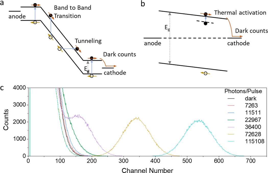
Understanding the origin of the dark counts in SiPMs helps us to design the photodetectors to reduce DCR. As shown in Fig. 1a, the DCR of SiPMs operating at high bias is dominated by band-to-band thermally generated carriers, and band-to-band tunneling24. Free carriers are frequently thermally generated and then accelerated by the large electric field in avalanche zone, causing counts even without incident photons. In addition, the large electric field in SiPMs can cause the direct tunneling of electrons from valance band to conduction band, which dominates the noise at temperature below 200 K.25 In this study, methylammonium lead iodide (MAPbI3) and methylammonium-formamidinium mixed cation perovskites (FA0.7MA0.3PbI3) were chosen for the self-powered PCDs because of its wider bandgap of >1.5 eV while maintaining the detection capability for UV-visible light. Its free carrier concentration caused by thermal excitation is 6–7 orders of magnitude smaller than that of silicon. The defect tolerance of perovskites may enable efficient charge extraction even at very low density of photoinduced charges. The perovskite PCDs are operated in photovoltaic mode at zero bias, i.e., the photo-generated carriers are extracted by the built-in field. The zero bias operation simplifies the read-out electronics and avoid the issue of ion migration. We speculate the DCR of perovskite PCDs is dominated by the thermal detrapping of trapped charges, as illustrated in Fig. 1b.
Fig. 1 |. Origin of dark counts and photon counting performance.
DCR contribution illustration for PCDs operated at high reverse bias for (a) SiPMs, (b) Zero bias for perovskite PCDs. The band tilting is not drawn in scale. (c) Output signal histograms of a typical MAPbI3 solar cell under incident light pulses with different photon numbers per pulse. The channel number is proportional to the extracted charges.
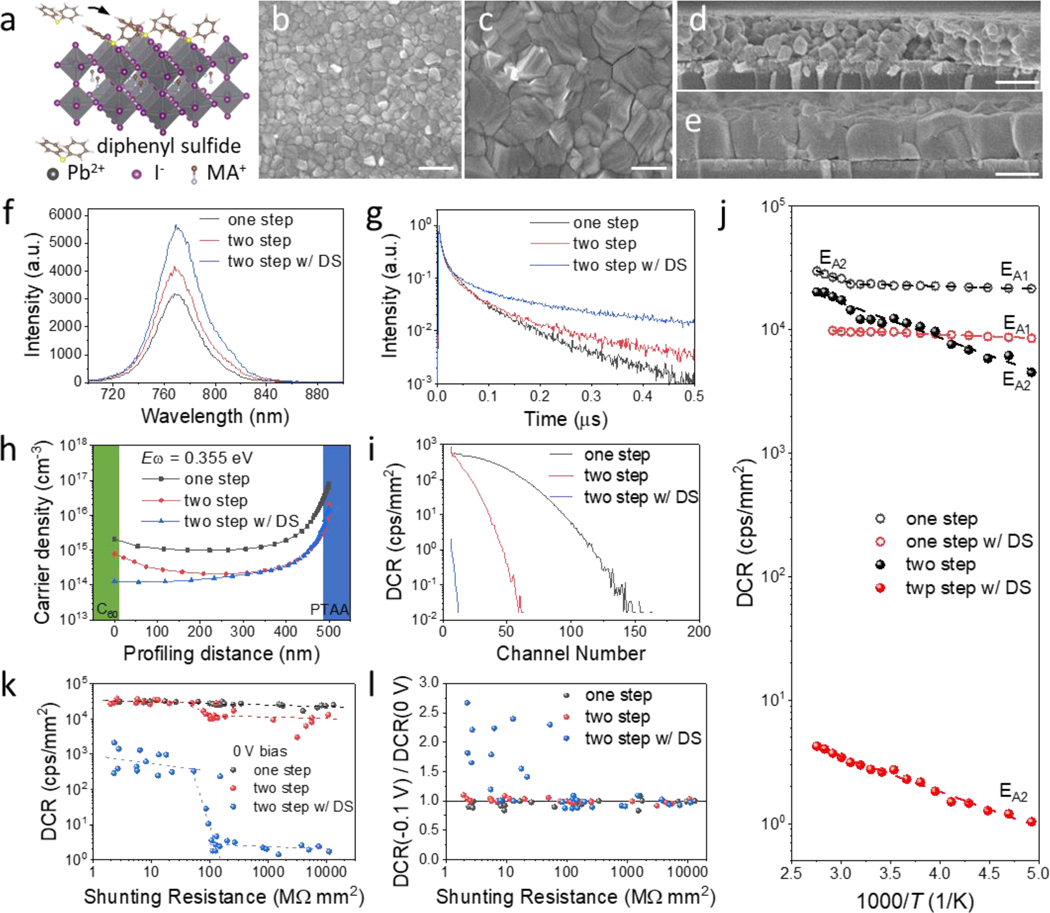
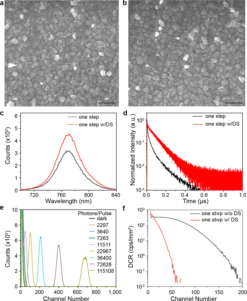
We first evaluated how strong the remission of trapped charges using optimized perovskite solar cells. The perovskite PCDs in this study have the same device structure with regular p-i-n structure solar cells of indium tin oxide (ITO)/poly(bis(4-phenyl)(2,4,6-trimethylphenyl)amine) (PTAA)/perovskite/C60/bathocuproine (BCP)/copper (Cu). The perovskite layer was either deposited by a one-step spin-coating followed by an antisolvent treatment (one-step), or using blading process followed by nitrogen knife drying, which can yield an efficiency of ~23.6% for FA0.7MA0.3PbI3 using our optimized additives and fabrication conditions11. The photocurrent density-voltage (J-V) curve of one typical device is shown in Extended Data Fig. 1a. The detector photon counting capability was evaluated using a measurement setup illustrated in Extended Data Fig. 1b. The incident photon number to PCDs was controlled by neutral density filters, and output pulse signal from PCDs was sequentially amplified, then recorded by multichannel analyzer (MCA), resulting in histograms of output amplitude. The FA0.7MA0.3PbI3 and MAPbI3 solar cells showed a high DCR of 23,467 and 23,732 cps/mm2, respectively, even the devices were operating at zero bias. The minimal detectable photon number, which is defined by the incident photon number that can cause a histogram distinguished from noise histogram, were 11,511 and 22,967 respectively, as shown in Fig. 1c and Extended Data Fig. 1c. This performance is still too poor for PCDs in application of γ-rays quanta detection. For example, a cesium iodide (triduum) (CsI(Tl)) scintillator exposed to 57Co (122 keV) γ-ray quanta generates 6588 photons. The very large DCR cannot be explained by band-to-band transition in MAPbI3 given its relatively large bandgap. Therefore, we speculate they are caused by the thermally activated carriers from charge traps. Prior studies showed that the deep-trapping defects mainly locate at the film surface26–28. To find out how such defects impact the DCR, we passivated the surface of MAPbI3 with diphenyl sulfide (Fig. 2a). Here diphenyl sulfide was chosen for surface passivation because of the relatively strong coordination of sulfur with lead. Unlike S2–, the S-Pb coordination using diphenyl sulfide is not so strong and thus won’t pull Pb out of the octahedral structure, which is evidenced by the maintained perovskite morphology after surface treatment (Extended Data Fig. 2a-b). Both steady-state photoluminescence (PL) and time-resolved PL (TRPL) measurement confirm that surface passivation is effective by the 44% stronger PL intensity and 36% longer PL lifetime (Extended Data Fig. 2c-d). However, the DCR was only reduced by 2.8 times after this surface treatment (Extended Data Fig. 2e–f), indicating these films still have a large density of defects in the bulk of the grains, at grain boundaries or at the embedded bottom interfaces.
Fig. 2 |. Suppressing DCR of perovskite PCDs.
(a) Schematic illustration of surface defect passivation by diphenyl sulfide. Top-view SEM images of (b) One-step processed MAPbI3 film and (c) Two-step processed MAPbI3 film. The scale bar is 500 nm. Cross-sectional SEM images of (d) One-step processed MAPbI3 film and (e) Two-step processed MAPbI3 film. Scale bar is 500 nm. (f) PL and (g) TRPL of MAPbI3 films on glass substrates. (h) Trap density at different profiling distance in the perovskite PCDs measured by DLCP at an AC frequency of 50 kHz. (i) DCR of perovskite PCDs. (j) Temperature dependent DCR of perovskite PCDs. (k) The shunting resistance and corresponded DCR of 32 one-step device, 30 two-step device, and 32 two-step devices with passivation. Each data point represents one device. (l) The ratio of DCR of each device biased at −0.1 V and 0 V.
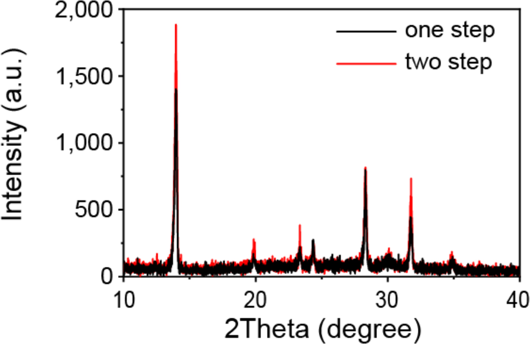
We then deposited perovskites using two-step process (two-step), because it was reported to form monolithic grains without many horizontal grain boundaries so that charges can be directly collected without encountering defective grain boundaries29,30. PbI2 was first deposited on HTL and then MAI was coated sequentially, followed by a thermal annealing so that they interdiffuse into each other to form perovskites31. An ultra-thin polymethyl methacrylate (PMMA) between the perovskite and PTAA layers was introduced to passivate the defects at the embedded interface32,33. The average grain size increased from 129 nm to 331 nm when we changed to the two-step process (Fig. 2b–c). The bigger perovskite grain size was clearly observed in the cross-sectional scanning electron microscope (SEM) images of the MAPbI3 film (Fig. 2e), showing monolithic grains. The X-ray diffraction (XRD) pattern in Extended Data Fig. 3 also shows that the two-step processed films have the stronger and sharper XRD peaks, suggesting a better crystallinity. Comparing to one-step processed film, the two-step processed film showed 30% stronger PL intensity, and the PL lifetime increased from 64 ns to 155 ns, indicating less defects in two-step MAPbI3 films.
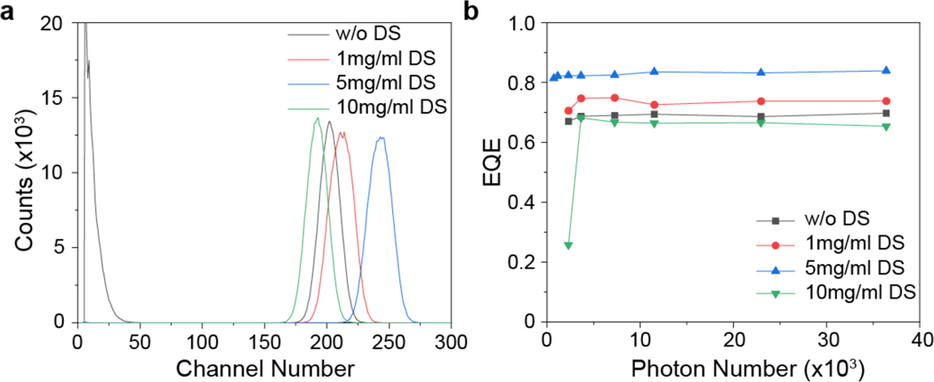
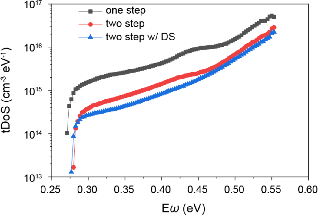
Since MAPbI3 made by two-step process needs a longer annealing (90 min) at a relatively high temperature, their surfaces are richer in defects due to the evaporation of MAI34,35. Therefore, we also conducted surface passivation using diphenyl sulfide (two-step with passivation). The concentration of diphenyl sulfide was optimized to achieve the highest charge collection efficiency based on the channel number of the photopeak (Extended Data Fig. 4). After surface passivation, the PL increased by 33%, and PL lifetime increased to 869 ns, as shown in Fig. 2f–g. The two-step detector had ~10 times lower trap density over the whole trap depth region than the one-step detector (Extended Data Fig. 5), and the surface treatment further halved the trap density. Drive-level capacitance profiling (DLCP) measurement (Fig. 2h) shows consistent result that the trap density was reduced by 9 times throughout the perovskite films using two-step process, and surface sulfurization further reduced the defect density mainly close to the top surface. The reduction of deep charge traps is accompanied with the reduction of DCR of the perovskite PCDs, however they do not show a good correlation. The integrated DCR was only reduced by half when the perovskite fabrication was changed to two-step process, while the followed surface treatment dramatically reduced the integrated DCR by 6,000 times to an ultra-small value of 2 cps/mm2 at room temperature (Fig. 2i), more than 1,000 times smaller than that of SiPMs measured in this study. The dramatically reduction of DCR came from not only the suppressed dark count rate but also the reduced amplitude of dark count events.
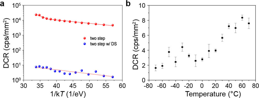
The lack of correlations between the DCR and deep trap density indicates the dark counts in perovskite PCDs may be caused by shallow traps. Calculating very shallow defects by density functional theory would be technically difficult. To experimentally find out the charge traps that determines DCR, we tested the temperature dependent DCR of perovskite PCDs, and derived the activation energy of the charge traps that induce dark counts from the slope of ln(DCR)~1/T. As shown in Fig. 2j, the one-step device exhibited one very shallow trap with activation energy (EA1) of 5.8±0.8 meV. It is so shallow that their thermal excitation at room temperature can easily reemit all trapped charges to the conduction band, which explains the very large DCR in these films. Another trap with an activation energy (EA2) of ~57 meV started to contribute to DCR at 50 °C. The 5.8 meV traps may mainly come from defects at grain boundaries, because surface passivation only slightly reduced the DCR. The surface passivation eliminated the traps of 57 meV, indicating it locates at film surface. The trap location assignment is further supported by the disappearance of the ultra-shallow traps in the two-step perovskite films with enhanced grain size. Instead, the two-step perovskite film has a dominating charge trap with EA2 of 57.2±0.1 meV. The density of this trap level was dramatically reduced by surface passivation using diphenyl sulfide, which again demonstrates that this defect mainly locates at the film surface. In some of the two-step perovskite films which were annealed for longer time, we observed a deep trap with a EA3 of ~190 meV (Extended Data Fig. 6a), which can also be passivated by diphenyl sulfide. This study concludes that the dark counts in perovskite PCDs are dominated by shallow traps either at grain boundaries or films surface, rather than deep ones, because deep ones don’t re-emit the trapped charges within the detection time range. These shallow traps clearly do not impact the efficiency of perovskite solar cells, but are detrimental to perovskite PCDs. Due to the small activation energy of charge traps, the DCR of the perovskite PCDs only changed from ~8 cps/mm2 to ~2 cps/mm2 in the temperature range of −70 °C to 70 °C (Extended Data Fig. 6b), which is a very desired property in applications so that a temperature controlling is not needed.
Although the average dark current of the devices operating at zero bias is zero, the fluctuation of dark current may still contribute to DCRs if the devices are shunted. We thus investigated the correlation between devices shunting resistance and DCR by measuring ~100 devices with different processes and passivation. Some of these devices showed obvious shunting behavior due to non-optimized fabrication process, but were still included to find out the impact of shunting to DCRs. The shunting resistance was determined by the inverse slope of the J-V curves at the 0 V (Extended Data Fig. 7)36. As shown in Fig. 2k, all the three types of devices showed a large variation of shunting resistance from a few MΩ mm2 to >10,000 MΩ mm2. The DCRs of all one-step devices are very high (27,941 ± 3,561 cps/mm2) and only slightly reduce with the increase of shunting resistance, indicating that the charge detrapping dominates the DCR. For two-step devices, DCR is ~32,020 ± 4,584 cps/mm2 for devices with shunting resistances less than 49.5 MΩ mm2, and slightly drops to 11,103 ± 3,358 cps/mm2 for devices with shunting resistance above 180 MΩ mm2. It shows that shallow trap density is still so large that the contribution from shunting is dimed even among the devices with very small shunting resistance. For the two-step devices with passivation, the detrapping induced dark counts is significantly suppressed so that the impact of shunting to DCRs became clearer: The DCR is 753 ± 579 cps/mm2 for the devices with shunting resistance less than 53 MΩ mm2, and the DCR declines with the increase of shunting resistance. The DCR sharply reduced to an almost constant value of 2.1 ± 1.0 cps/mm2 for devices with shunting resistance above 146 MΩ mm2, a sign that the DCR is only determined by detrapping process. Furthermore, we applied a small bias of −0.1 V to the devices which should increase shunting due to the increased leakage current but have negligible impact to the charge detrapping process. Fig. 2l showed the ratio of DCRs of each device measured at −0.1 V and 0 V. The DCR ratio equals to 1 when the DCR is dominated by charges detrapping process, and exceeds 1 when shunting dominates. It further confirms that the DCRs of the optimized perovskite PCDs are caused by detrapping of trapped charges from shallow traps, and the two-step fabrication process in combination with surface sulfurization is effective in reducing the shallow traps in perovskite films. In this context, the difficulty of doping perovskites, in striking contrast to many other inorganic semiconductors, contributes to the very low DCR of the perovskite PCD.
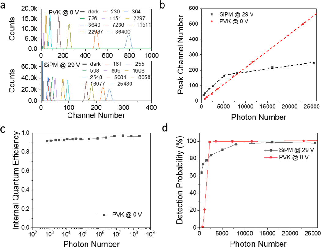
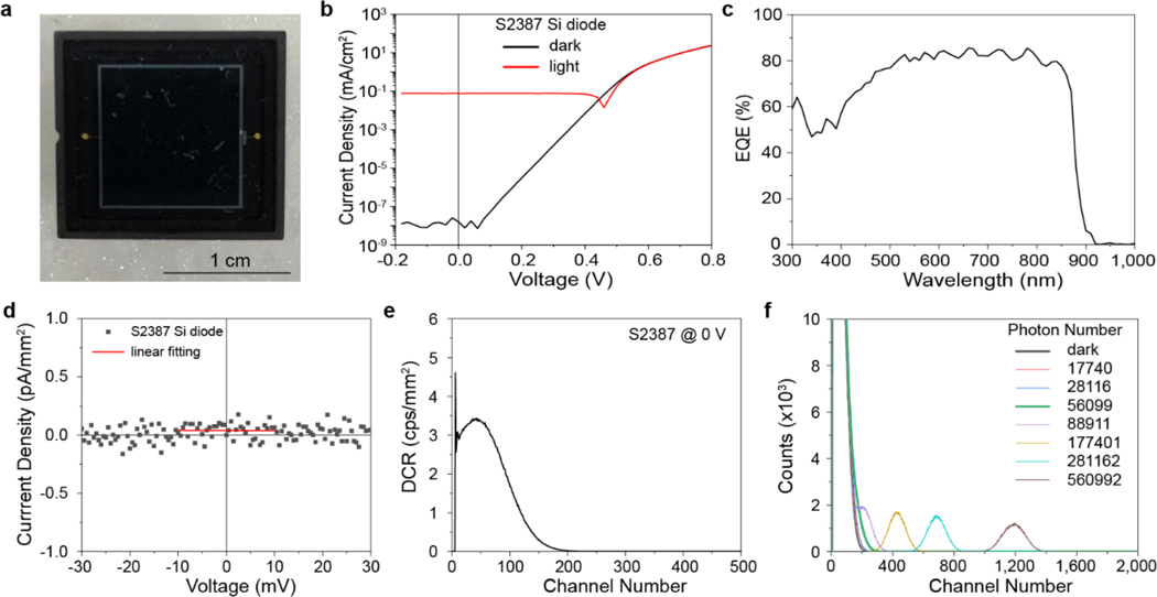
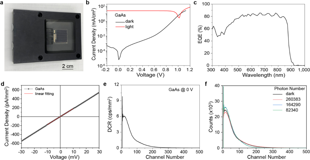
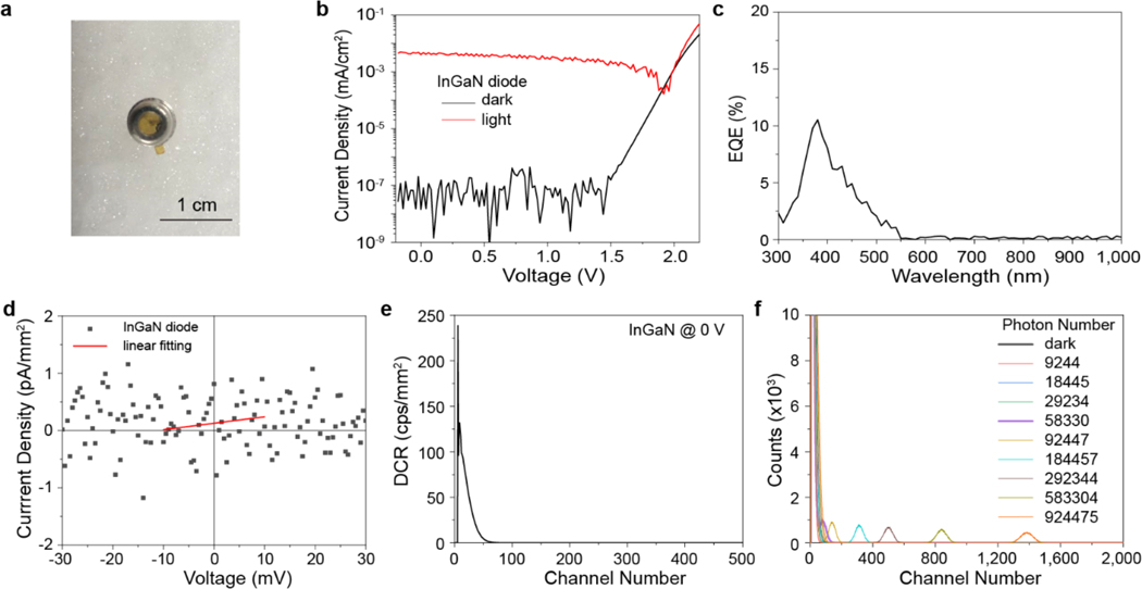
The photon counting performance of the zero-biased perovskite PCDs was further examined and compared with a commercial SiPM operated at 29 V, and commercial single crystalline Si, GaAs and InGaN photodiodes at 0 V (Fig. 3a and Extended Data Fig. 8–10). The perovskite PCD demonstrated the minimal detectable photon number of 726, which is good enough to count the photons from CsI(Tl) scintillator exposed to 57Co γ-rays. The Si photodiode, GaAs photodiode, and InGaN diode showed a much larger minimal detectable photon number of 56,099, >260,383, and 29,234 respectively, despite that they have larger shunting resistance and/or wider bandgap. These results show that perovskite PCDs are superior to regular inorganic crystalline photodiodes for photon counting application, contributed by their unusual defect tolerance and low shallow trap density after passivation.
Fig. 3 |. Perovskite detector photon counting performance.
(a) Output signal histograms of zero-biased perovskite PCD and SiPM operating at 29 V under the various number of incident photons per pulse. The unit is photons/pulse. (b) Channel number of the photopeak at different incident photon numbers per pulse. (c) Internal quantum efficiency of the perovskite PCD at different incident photons per pulse. (d) Pulse detection probability of the perovskite PCD and the SiPM.
We derived the linearity of the SiPM and perovskite PCDs by plotting the photopeak channel number with the incident photons number. The SiPM showed two linear regions, limiting its photon counting capability (Fig. 3b), while the perovskite PCD had only one straight linearity region. To evaluate the linearity response at a wider range, the internal quantum efficiency (IQE) of perovskite PCD was evaluated with up to 229 million photons per light pulse. The perovskite PCD had a constant IQE of 95±5% from 726 photons to >108 photons, as shown in Fig. 3c. The huge linear dynamic range of the perovskite PCD should be ascribed to the low deep defect density, which contributes to the good linear response under weak light, and low charge recombination in perovskites, which contributes to the linear response under strong light. The pulse detection probability, defined as the probability that an incident light pulse generates an output pulse, was directly measured for perovskite and SiPM PCDs. As shown in Fig. 3d, the pulse detection probability of the SiPM increased from 73.8% to 96.6% when the incident photons number increased from 806 to 8,058 and saturated at ~99% for stronger light pulse. In striking contrast, the perovskite detector exhibited a nearly constant pulse detection probability of >99.8% when each light pulse has 1,600 or more photons. Therefore, perovskite PCDs can count ~15% more pulses than the SiPM when photon number per event is less than 8,058.
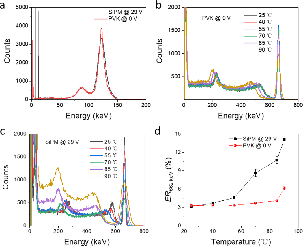
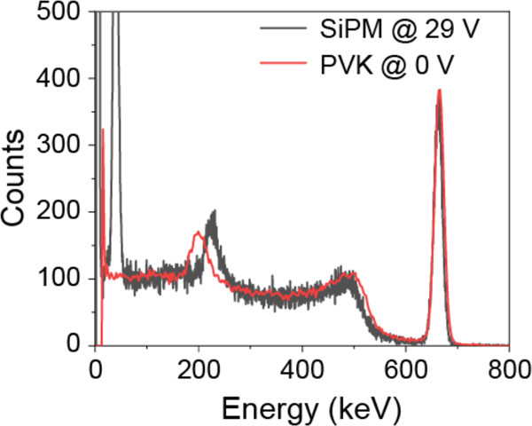
The superior photon counting capability of the perovskite PCDs makes them a promising candidate as γ-ray spectroscopy when combined with scintillators. Here, we coupled perovskite PCDs with a cerium doped lanthanum bromide (LaBr3:Ce) scintillator, which is one of the brightest scintillators and emission centered around 380 nm, well covered by the perovskite PCDs. The 57Co γ-ray energy spectra collected by the SiPM and the perovskite PCD under the same conditions were showed in Fig. 4a. The perovskite PCD showed 16.3% more counts during the same acquisition time, and the energy resolution of 9.3±0.17% at 122 keV is better than that of the SiPM (11.34±0.27%). For high energy γ-ray photons, the perovskite PCDs gave a comparable energy resolution of 3.2±0.1% at 662 keV (Extended Data Fig. 11), which can be explained by their comparable photon counting probability under strong light. To evaluate the capability of the PCDs at harsh environment, 137Cs γ-ray energy spectra were collected by the perovskite and the SiPM PCDs at temperature from 25 °C to 90 °C. As shown in Fig. 4b, the spectra collected by the perovskite PCD almost overlapped when temperature was lower than 70 °C. The photopeak broadened slightly when the temperature further increased, which may be caused by the reduced light yield of LaBr3:Ce at higher temperature37, while the photopeak broadening was very small at the temperature < 90 °C. In contrast, the energy resolution of the spectra collected by the SiPM obviously changed from 3.1% to above 10% when the temperature increased to above 85 °C (Fig. 4c–d). This clearly shows the advantage of perovskite PCDs in working at much harsher environment.
Fig. 4 |. Perovskite PCDs coupled with the LaBr3:Ce scintillator γ-ray spectroscopy performance.
(a) 57Co γ-ray spectra collected by the perovskite PCD and the SiPM under the same experimental conditions. 137Cs γ-ray spectra collected by (b) the perovskite PCD and (c) the SiPM, and (d) Energy resolution at 662 keV resolved by the perovskite PCD and the SiPM at different temperatures, the error bars represented 5% errors from the Gaussian fitting.
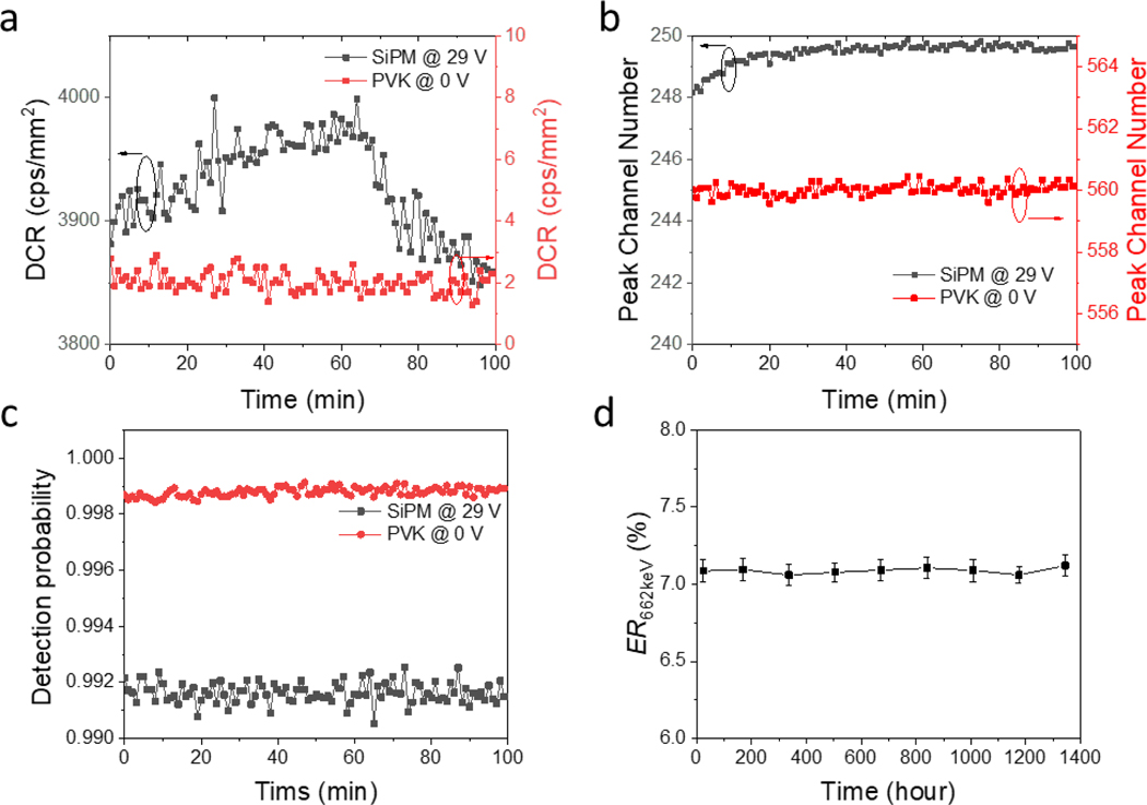
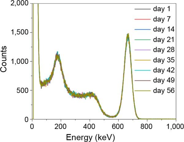
Operating the perovskite PCDs at zero bias also brings the unprecedented small drift of device performance over time, because it avoids the large electric field induced device degradation or material change. To demonstrate that, the DCR of the perovskite detector at zero bias and the SiPM at 29 V were acquired for multiple cycles without temperature controlling (Fig. 5a). The DCR of the SiPM is not only high, but also fluctuated by 185 cps/mm2. In striking contrast, the perovskite PCD exhibited a nearly constant and very small DCR of 2 cps/mm2. The response stability of the PCDs was measured by illuminating them with light pulses. The SiPM output photopeak channel number drifted from 248 to 250 after 30 min, while the perovskite PCDs had nearly no drifting (Fig. 5b). The perovskite PCD and the SiPM have pulse detection probability of 99.97±0.02% and 99.16±0.37% respectively within 100 min tracking (Fig. 5c). In addition, the long-term stability was evaluated by tracking the 137Cs γ-ray spectrum energy resolution. As shown in Fig. 5d, the energy resolution at 662 keV kept unchanged within 8 weeks for the perovskite PCD coupled with CsI(Tl) scintillator, and the measured spectra almost overlapped (Extended Data Fig. 12).
Fig. 5 |. Perovskite PCDs stability.
The tracking of (a) DCR, (b) the output histogram peak channel number under continuous 25,685 photons/pulse. (c) Pulse detection probability for incident photon number of 25,685 per pulse of the perovskite PCD at zero bias and the SiPM at 29 V. (d) the 137Cs γ-ray spectrum energy resolution resolved by the perovskite PCD coupled with CsI(Tl) at zero bias, the error bars represented 5% errors from the Gaussian fitting.
In summary, we found that the DCR of perovskite PCDs was dominated by charge detrapping from shallow traps located at the grain boundaries and surface, and the ultra-low DCR was achieved by suppressing the shallow traps by enhancing grain size and passivating film surface with diphenyl sulfide. The suppression of shallow trap made the perovskite PCDs have 100–1,000 times lower DCR and much better response linearity to weak light than SiPMs, and the DCR was not sensitive to temperature due to small activation energy of charge traps. The zero-bias operating perovskite PCDs were demonstrated as γ-ray spectrum detectors with better energy resolution under 57Co source than commercial SiPMs at room temperature. At higher temperature up to 85 °C, the perovskite PCDs are much superior to SiPMs by maintaining the energy resolution, showing their potential of working in harsh environment. This study discovered regular surface passivation also dramatically impact shallow charge traps, which should have implication of perovskite stability and doping.
Methods
Materials:
Chemicals in this work were used as received. PTAA (average Mn 7,000–10,000), PMMA (average Mn 120,000), dimethyl sulfoxide (DMSO), dimethylformamide (DMF), acetonitrile, toluene, diphenyl sulfide (DS), and isopropanol (IPA) were purchased from Sigma-Aldrich. MAI and FAI were purchased from GreatCell Solar. PbI2 was purchased from Tokyo Chemical Industry CO., LTD.
Device fabrication:
patterned ITO glass substrates were cleaned with detergent, acetone, and IPA in sequence and then treated with UV-ozone for 15 min. A PTAA solution with a concentration of 2 mg/ml in toluene was spin-coated onto the ITO substrate at 4000 rounds per minute (rpm) for 30 s, and the as-prepared PTAA film was annealed at 100 °C for 10 min. For MAPbI3 films deposited by the two-step process: a PMMA solution with a concentration of 0.5 mg/ml in acetonitrile was spin-coated on the PTAA layer at 5000 rpm for 30 s, and the as-prepared PMMA film was annealed at 100 °C for 10 min. PbI2 and MAI were dissolved in DMF and IPA with concentrations of 630 mg/ml and 65 mg/ml respectively. The PbI2 solution was spin-coated onto the PTAA layer at 3000 rpm for 30 s and then annealed at 100 °C for 10 min. The MAI solution was spin-coated on the PbI2 film at 3000 rpm for 30 s. The perovskite was obtained by annealing the stacked layers at 100 °C for 90 min. For MAPbI3 films deposited by the one-step process: PbI2 and MAI were dissolved into DMF and DMSO (with a volume ratio of 9:1) with a concentration of 1.3 M to obtain the MAPbI3 precursor solution. 50 μl MAPbI3 solution was spin-coated on the PTAA layer at 2000 rpm for 3 s and then 4000 rpm for 19 s, and 130 μl toluene was added to film during the spin-coating. The as-formed film was then annealed at 100 °C for 10 min. For FA0.7MA0.3PbI3 devices, the films were deposited by the method described in our previous work11. For diphenyl sulfide surface treatment, a 5 mg/ml diphenyl sulfide solution in IPA was spin-coated on the MAPbI3 layer at 5000 rpm for 30 s, and then annealed at 100 °C for 10 min. Then 100 nm thick C60, 6 nm thick BCP, and 180 nm Cu were sequentially deposited on the MAPbI3 layer by thermal evaporation, and the device area was defined by the overlapping of Cu electrode and ITO. All devices in this study have an active area of 1×1 mm2. The completed devices were encapsulated with cover glass sealed by an epoxy encapsulant (Devcon 14210).
Photon counting performance measurement:
the incident light was from a picosecond laser diode head (Horiba DD-635L) with a wavelength of 630 nm, and the laser head was driven by a Horiba DD-C1 controller, which was triggered by a pulse signal with a repetition frequency of 5 kHz generated by an oscilloscope (Agilent DSO-X 3104A). The incident photon number (N) to detectors was controlled by neutral density filters (Thorlabs), and can be calculated through N = Plaser/ flaser ×10-OD×λ/hc, where Plaser is laser initial power, flaser is pulse repetition frequency, OD is the optical density of the neutral density filters, and λ is the wavelength of the laser. The detector output pulse signal was sequentially amplified by a charge sensitive preamplifier that has a gain of 1.1 mV/fC (Kromek Ltd, ev-550/ev-5094) and a shaping amplifier that has a gain of 1,000x and a shaping time of 6 μs (Ortec, 572A), then record by an MCA (Ortec, easy-MCA). The charge sensitive preamplifier was not used when a SiPM was used as the photodetector, since it has intrinsic gain. The SiPM is Mircrofj-60035-TSV from Onsemi with an active area of 6.07×6.07 mm2. Perovskite PCDs were measured at zero bias. For temperature dependent DCR measurement, the device temperature was controlled by the Linkam microscope temperature stage (LTS420), and the DCR measurements were taken after holding the device at the set temperature for 15–20 min. Five DCR histograms were collected at each temperature to calculate the average DCR for activation energy fitting.
Devices characterizations:
The SEM images were taken on an FEI Helois 600 nanolab dual beam system. The 5 kV at low vacuum mode was applied for characterization. Photoluminescence and TRPL were conducted using a FluoTime 300 system from PicoQuant. The excitation wavelength was 485 nm. The laser power was 0.198 mW with a frequency of 20 MHz for PL measurement, and 0.216 μW with a frequency of 0.02 MHz for TRPL measurement. The XRD was characterized by Rigaku SmartLab. The I-V curves for shunting resistance determination were acquired by a Keithley 4200A-SCS in the dark, and the noise floor of I-V measurement system is characterized at open-circuit using same parameters as devices twice (Extended Data Fig. 7b). The current fluctuation is in the range of 1.52 pA to 2.04 pA for the measurement system, and the current fluctuation of the one step, two step and two-step with passivation devices in the range of −2.5 mV to 2.5 mV is 1.51 pA, 1.98 pA, and 1.76 pA respectively, indicating that the current fluctuation of perovskite detectors I-V curves in Extended Data Fig. 7a is mainly from the measurement system noise. The tDOS of perovskite detectors were derived from the frequency-dependent capacitance (C-f), which was from the thermal admittance spectroscopy (TAS) measurement performed by an LCR meter (Agilent E4980A). For DLCP measurement, the DC bias scanned from 0 V to the open-circle voltage (e.g. 1.1 V) for the perovskite detectors. The DLCP method uses a series of variable δV (for example, 20–200 mV) to measure the junction capacitance and acquire the capacitance contribution from the trap states by taking advantage of the information embedded in the higher-order terms. The capacitance measured at each δV was recorded and fitted with a polynomial function C = C0 + C1δV + C2(δV)2 + … to obtain C0 and C1. With the determination of C0 and C1, the total carrier density (N) that includes both free carrier density and trap density at the profiling distance X from the junction barrier is calculated by N = -C03/(2qεA2C1), in which is the elementary charge, ε is the dielectric constant, which is 31 for MAPbI3, and A is the active area of the junction. The profiling distance from the junction barrier was calculated by , which was changed by tuning the DC bias. For each AC bias, an additional offset DC voltage was applied to keep the maximum forward bias constant. All tDOS and DLCP measurements were finished in dark conditions.
Internal quantum efficiency:
The reflectivity (R) at 630 nm was measured using Lambda 1050 UV-Vis spectrophotometer. And the internal quantum efficiency was calculated by IQE = EQE/(1-R), in which EQE is external quantum efficiency. Since the MCA has 2048 channels and is saturated by a 14.2 V input bias, the collected charge number was derived by Ncharge = Channel number×14.2×10⁻¹⁵/(2048×1.1×e) for photon number below 2.41×10⁶, in which is the elementary charge. For photon number above 7.63×10⁶, the collected charge number was derived from charge amplifier output amplitude (Vchanrge amplifier in mV) by Ncharge = Vchanrge amplifier×10−15/(1.1×e), The EQE was obtained by EQE = Ncharge/Nincident photon, where Nincident photon is the incident photon number.
Gamma-ray spectrum measurement:
the γ-ray sources employed here were 1 μCi 137Cs 662 keV and 1 μCi 57Co 122 keV. The detectors were coupled with the LaBr3:Ce scintillator (dimensions of Φ10×14 mm3 from Kinheng Crystal Material (Shanghai) Co.,ltd.) using a polydimethylsiloxane film as coupling layer. The detectors coupled with scintillator and the γ-ray source were put in an aluminum shied box. The perovskite detectors were measured at zero bias, and the SiPM was measured at 29 V. The detector output signal was sequentially amplified by a charge sensitive preamplifier (Kromek Ltd, ev-550/ev-5094) and a shaping (Ortec, 572A) amplifier with a gain of 1000x and shaping time of 6 μs, then record by an MCA (Ortec, easy-MCA). The charge sensitive preamplifier was not used when the SiPM was used as detector. For temperature dependent γ-ray spectra collection, the detectors coupled with scintillator were put in a muffle furnace, and spectra were collected after holding them at set temperature for 30 min.
Stability measurement:
the dark count rate stability, photon response stability and pulse detection probability stability were conducted by the same system as photon counting performance measurement. The output histogram was acquired with 10 s continuous recording followed by an interval of 50 s. For DCR stability characterization, the DCR was calculated from the total counts in each cycle divided by the acquisition duration. For photon response stability and pulse detection probability stability, the light continuously illuminated the devices during the measurement. For long-term stability, the 137Cs γ-ray spectrum was collected once per week using the same perovskite PCD coupled with the CsI(Tl) scintillator under the same experimental conditions.
Extended Data
Extended Data Fig. 1 |. Photon-counting performance of a typical FA0.7MA0.3PbI3 solar cell.
(a) typical J-V curve of FA0.7MA0.3PbI3 solar cell. (b) Schematic diagram of the photon counting measurement system, CSP is charge sensitive preamplifier. (c) photon counting performance of the FA0.7MA0.3PbI3 solar cell.
Extended Data Fig. 2 |. Diphenyl sulfide surface passivation.
SEM images of perovskite films (a) without and (b) with diphenyl sulfide surface passivation. Scale bar is 500 nm. (c) PL spectra and (d) TRPL of MAPbI3 films on glass deposited by one-step process with and without diphenyl sulfide passivation. (e) photon counting performance of one-step processed MAPbI3 with diphenyl sulfide passivation. (f) DCR of one-step processed MAPbI3 devices with and without diphenyl sulfide passivation.
Extended Data Fig. 3 |. XRD patterns of MAPbI3 films.
The XRD patterns of the one-step and two-step processed perovskite films.
Extended Data Fig. 4 |. Photon counting performance of two-step MAPbI3 devices with different passivation concentration.
(a) Response for 11,511 photons/pulse (b) EQE of devices with various diphenyl sulfide surface passivation concentration.
Extended Data Fig. 5 |. tDOS of the perovskite PCDs.
The tDOS of perovskite PCDs fabricated by one-step, two-step, and two-step with passivation processes, measured by TAS for the devices in the dark.
Extended Data Fig. 6 |. Temperature dependent DCR.
(a) Temperature dependent DCR of two-step with passivation perovskite PCDs annealed for longer time. (b) Temperature dependent DCR of a typical two-step with passivation perovskite PCD. The error bars are standard deviation of triplicate measurements.
Extended Data Fig. 7 |. Shunt resistance of the perovskite PCDs.
(a) Dark current curves of the one-step, two-step and two-step with passivation MAPbI3 devices. The solid lines are the fitting lines to extract the shunt resistance. The shunt resistances of one-step, two-step, and two-step with passivation MAPbI3 devices is 10,964 MΩ mm2, 8,887 MΩ mm2 and 9,523 MΩ mm2, respectively. The I-V curves for shunting resistance determination were acquired by a Keithley 4200A-SCS in the dark. (b) Noise floor of the I-V measurement system. The noise floor was measured by removing the device to sweep the I-V measurement..
Extended Data Fig. 8 |. Performance of the silicon diode (S2387 from Hamamatsu).
(a) A photograph of the silicon S2387 diode; (b) Photo and dark current density curves of the Si photodiode. (c) EQE of the Si photodiode. (d) shunting resistance of the photodiode. (e) Dark count rate collected for the photodiode detector for 60 s measured at zero bias. (f) Output of the Si diode measured at zero bias under incident light pulse with photon numbers. The light source for the photon counting performance measurement is a 630 nm picosecond pulse laser from Horiba.
Extended Data Fig. 9 |. Performance of the monocrystalline GaAs photodetector.
(a) A photograph of the single crystalline GaAs solar cells. (b) Photo and dark current density curves of the GaAs solar cell; (c) EQE of the GaAs solar cells. (d) shunting resistance of the GaAs solar cells. (e) Dark count rate collected for the GaAs detector for 60 s measured at zero bias. (f) Output of the GaAs detectors measured at zero bias under incident light pulse with photon numbers upto 260,383. The light source for the photon counting performance measurement is a 630 nm picosecond pulse laser from Horiba.
Extended Data Fig. 10 |. Performance of the InGaN PN diode (GVGR-T11GD from GENUV, Inc.).
(a) A photograph of the InGaN diode. (b) Photo and dark current density curves of the InGaN diode. (c) EQE of the InGaN diode. (d) shunting resistance of the InGaN photodiode. (e) Dark count rate collected for the detector for 60 s measured at zero bia.; (f) Output of the InGaN diode measured at zero bias under incident light pulse with photon numbers. The light source for the photon counting performance measurement is a 404 nm picosecond pulse laser from Horiba.
Extended Data Fig. 11 |. Spectra collected by PCDs coupled with the LaBr3:Ce scintillator.
137Cs γ -ray spectra collected by the perovskite PCD at zero bias and SiPM at 29 V under the same experimental conditions.
Extended Data Fig. 12 |. Stability study of the perovskite PCDs coupled with the CsI(Tl) scintillator.
137Cs γ -ray spectra collected by the perovskite PCD at zero bias under the same experimental conditions once per week in 8 weeks.
Acknowledgement
This work was mainly supported by the Department of the Defense, Defense Threat Reduction Agency under Grant No. HDTRA1–20-2–0002. We thank the support from National Institutes of Health under award 1R01EB033439 for the characterization of scintillators using the perovskite PCDs. The device fabrication work was supported in part by U.S. Department of Energy’s Office of Energy Efficiency and Renewable Energy (EERE) under Solar Energy Technologies Office (SETO) Agreement Number DE-EE0009520. The defect characterization was supported in part by the Center for Hybrid Organic Inorganic Semiconductors for Energy (CHOISE), an Energy Frontier Research Center funded by the Office of Basic Energy Sciences, Office of Science within the US Department of Energy. The views expressed herein do not necessarily represent the views of the U.S. Department of Energy or the United States Government.
Footnotes
Competing interests
The authors declare no competing financial interests.
Data availability
All data generated or analyzed during this study are included in the article and its Extended Data.
References
- 1.Gundacker S. & Heering A. The silicon photomultiplier: fundamentals and applications of a modern solid-state photon detector. Physics in Medicine & Biology 65, 17TR01 (2020). [DOI] [PubMed] [Google Scholar]
- 2.Ye M. et al. Lightweight SiPM-based CeBr3 gamma-ray spectrometer for radiation-monitoring systems of small unmanned aerial vehicles. Applied Radiation and Isotopes 176, 109848 (2021). [DOI] [PubMed] [Google Scholar]
- 3.Agishev R. et al. Lidar with SiPM: some capabilities and limitations in real environment. Optics & Laser Technology 49, 86–90 (2013). [Google Scholar]
- 4.Hadfield RH Single-photon detectors for optical quantum information applications. Nature Photonics 3, 696–705 (2009). [Google Scholar]
- 5.Eraerds P, Legré M, Rochas A, Zbinden H. & Gisin N. SiPM for fast photon-counting and multiphoton detection. Optics Express 15, 14539–14549 (2007). [DOI] [PubMed] [Google Scholar]
- 6.Del Guerra A. et al. Advantages and pitfalls of the silicon photomultiplier (SiPM) as photodetector for the next generation of PET scanners. Nuclear Instruments and Methods in Physics Research Section A: Accelerators, Spectrometers, Detectors and Associated Equipment 617, 223–226 (2010). [Google Scholar]
- 7.Buzhan P. et al. in Advanced technology and particle physics 717–728 (World Scientific, 2002). [Google Scholar]
- 8.Du J. et al. Characterization of large-area SiPM array for PET applications. IEEE transactions on nuclear science 63, 8–16 (2016). [DOI] [PMC free article] [PubMed] [Google Scholar]
- 9.Engelmann E, Popova E. & Vinogradov S. Spatially resolved dark count rate of SiPMs. The European Physical Journal C 78, 1–8 (2018). [Google Scholar]
- 10.Fleck I, Titov M, Grupen C. & Buvat I. Handbook of Particle Detection and Imaging. (Springer, 2019). [Google Scholar]
- 11.Chen S. et al. Stabilizing perovskite-substrate interfaces for high-performance perovskite modules. Science 373, 902–907 (2021). [DOI] [PubMed] [Google Scholar]
- 12.Lin K. et al. Perovskite light-emitting diodes with external quantum efficiency exceeding 20 per cent. Nature 562, 245–248 (2018). [DOI] [PubMed] [Google Scholar]
- 13.Fang Y, Dong Q, Shao Y, Yuan Y. & Huang J. Highly narrowband perovskite single-crystal photodetectors enabled by surface-charge recombination. Nature Photonics 9, 679–686 (2015). [Google Scholar]
- 14.Zhao J. et al. Perovskite-filled membranes for flexible and large-area direct-conversion X-ray detector arrays. Nature Photonics 14, 612–617 (2020). [Google Scholar]
- 15.Luo J. et al. Water photolysis at 12.3% efficiency via perovskite photovoltaics and earth-abundant catalysts. Science 345, 1593–1596 (2014). [DOI] [PubMed] [Google Scholar]
- 16.Deng Y. et al. Tailoring solvent coordination for high-speed, room-temperature blading of perovskite photovoltaic films. Science advances 5, eaax7537 (2019). [DOI] [PMC free article] [PubMed] [Google Scholar]
- 17.Ávila J, Momblona C, Boix PP, Sessolo M. & Bolink HJ Vapor-deposited perovskites: the route to high-performance solar cell production? Joule 1, 431–442 (2017). [Google Scholar]
- 18.Dong Q. et al. Electron-hole diffusion lengths> 175 μm in solution-grown CH3NH3PbI3 single crystals. Science 347, 967–970 (2015). [DOI] [PubMed] [Google Scholar]
- 19.Wei H. et al. Sensitive X-ray detectors made of methylammonium lead tribromide perovskite single crystals. Nature Photonics 10, 333–339 (2016). [Google Scholar]
- 20.Stranks SD et al. Electron-hole diffusion lengths exceeding 1 micrometer in an organometal trihalide perovskite absorber. Science 342, 341–344 (2013). [DOI] [PubMed] [Google Scholar]
- 21.Shi D. et al. Low trap-state density and long carrier diffusion in organolead trihalide perovskite single crystals. Science 347, 519–522 (2015). [DOI] [PubMed] [Google Scholar]
- 22.Bao C. et al. Low-noise and large-linear-dynamic-range photodetectors based on hybrid-perovskite thin-single-crystals. Advanced Materials 29, 1703209 (2017). [DOI] [PubMed] [Google Scholar]
- 23.Fang Y. & Huang J. Resolving weak light of sub-picowatt per square centimeter by hybrid perovskite photodetectors enabled by noise reduction. Advanced Materials 27, 2804–2810 (2015). [DOI] [PubMed] [Google Scholar]
- 24.Panglosse A. et al. Dark count rate modeling in single-photon avalanche diodes. IEEE Transactions on Circuits and Systems I: Regular Papers 67, 1507–1515 (2020). [Google Scholar]
- 25.Liu F. et al. Characterization of a mass-produced SiPM at liquid nitrogen temperature for CsI neutrino coherent detectors. Sensors 22, 1099 (2022). [DOI] [PMC free article] [PubMed] [Google Scholar]
- 26.Chen S. et al. Identifying the soft nature of defective perovskite surface layer and its removal using a facile mechanical approach. Joule 4, 2661–2674 (2020). [Google Scholar]
- 27.Li X. et al. Constructing heterojunctions by surface sulfidation for efficient inverted perovskite solar cells. Science 375, 434–437 (2022). [DOI] [PubMed] [Google Scholar]
- 28.Wu W-Q et al. Reducing surface halide deficiency for efficient and stable iodide-based perovskite solar cells. Journal of the American Chemical Society 142, 3989–3996 (2020). [DOI] [PubMed] [Google Scholar]
- 29.Shen L. et al. A self-powered, sub-nanosecond-response solution-processed hybrid perovskite photodetector for time-resolved photoluminescence-lifetime detection. Advanced Materials 28, 10794–10800 (2016). [DOI] [PubMed] [Google Scholar]
- 30.Shen L. et al. Integration of perovskite and polymer photoactive layers to produce ultrafast response, ultraviolet-to-near-infrared, sensitive photodetectors. Materials Horizons 4, 242–248 (2017). [Google Scholar]
- 31.Lee J-W & Park N-G Two-step deposition method for high-efficiency perovskite solar cells. MRS Bulletin 40, 654–659 (2015). [Google Scholar]
- 32.Zhang F. et al. Comprehensive passivation strategy for achieving inverted perovskite solar cells with efficiency exceeding 23% by trap passivation and ion constraint. Nano Energy 89, 106370 (2021). [Google Scholar]
- 33.Wang J. et al. Front-contact passivation of PIN MAPbI3 solar cells with superior device performances. ACS Applied Energy Materials 3, 6344–6351 (2020). [Google Scholar]
- 34.Turren-Cruz S-H, Hagfeldt A. & Saliba M. Methylammonium-free, high-performance, and stable perovskite solar cells on a planar architecture. Science 362, 449–453 (2018). [DOI] [PubMed] [Google Scholar]
- 35.Zheng X. et al. Defect passivation in hybrid perovskite solar cells using quaternary ammonium halide anions and cations. Nature Energy 2, 1–9 (2017). [Google Scholar]
- 36.Thompson PR & Larason TC in Measurement Science Conference. [Google Scholar]
- 37.Choi Y, Kim KJ, Park K. & Kim Y. A LaBr3 (Ce) detector system with a simple spectral shift correction method for applications in harsh environments. Radiation Measurements 142, 106567 (2021). [Google Scholar]
Associated Data
This section collects any data citations, data availability statements, or supplementary materials included in this article.
Data Availability Statement
All data generated or analyzed during this study are included in the article and its Extended Data.


