

Abstract
A cryogenic variable-temperature ultra-high vacuum scanning tunneling microscope is used for measuring the electrical properties of isolated cyclopentene molecules adsorbed to the degenerately p-type Si(100)-2×1 surface at a temperature of 80 K. Current–voltage curves taken under these conditions show negative differential resistance at positive sample bias, in agreement with previous observations at room temperature. Because of the enhanced stability of the scanning tunneling microscope at cryogenic temperatures, repeated measurements can be routinely taken over the same molecule. Taking advantage of this improved stability, we show that current–voltage curves on isolated cyclopentene molecules are reproducible and possess negligible hysteresis for a given tip–molecule distance. On the other hand, subsequent measurements with variable tip position show that the negative differential resistance voltage increases with increasing tip–molecule distance. By using a one-dimensional capacitive equivalent circuit and a resonant tunneling model, this behavior can be quantitatively explained, thus providing insight into the electrostatic potential distribution across a semiconductor-molecule-vacuum-metal tunnel junction. This model also provides a quantitative estimate for the alignment of the highest occupied molecular orbital of cyclopentene with respect to the Fermi level of the silicon substrate, thus suggesting that this experimental approach can be used for performing chemical spectroscopy at the single-molecule level on semiconductor surfaces. Overall, these results serve as the basis for a series of design rules that can be applied to silicon-based molecular electronic devices.
Keywords: cyclopentene, resonant tunneling, molecular electronics, capacitance, spectroscopy
Since the seminal paper of Aviram and Ratner (1), the field of molecular electronics has undergone rapid growth. Many research efforts are probing the unique charge-transport properties of individual molecules with hopes of revolutionizing electronics and computation. A common experimental approach in this field is to vary the structure of the organic molecule that is placed between two metal electrodes (2–14). However, recent reports suggest that the contacts themselves play a pivotal role in the observed charge-transport behavior of several of these devices (15). This development suggests that, in addition to different molecular systems, alternative contact materials may lead to unique electronic functionality. Because of its compatibility with organic chemistry, its semiconductor band structure, and its ubiquity in commercially available microelectronics, silicon is a promising alternative substrate for molecular electronics.
Concurrent with the recent developments in molecular electronics, the ultra-high vacuum (UHV) scanning tunneling microscope (STM) has advanced well beyond its original purpose of probing the structure and properties of materials at atomic length scales (16). Atom manipulation (17–21), nanolithography (22–25), chemical modification (26, 27), and spectroscopy (28) are among the several advancements seen within the field of STM. In particular, the ability to probe individual molecules with atomic precision makes the STM an ideal tool for studying molecular electronics. Consequently, in this paper, we quantitatively explore the prospects for silicon-based molecular electronics by using cryogenic variable-temperature UHV STM.
We have previously reported the study of charge transport through organic molecules covalently bound to silicon surfaces with room-temperature UHV STM (29–31). These initial experimental studies revealed doping-dependent unipolar negative differential resistance (NDR) in the current–voltage curves on individual molecules. The observation of NDR qualitatively agrees with a theoretical model proposed by Rakshit et al. (32), which predicts that a semiconductor-molecule-vacuum-metal tunnel junction will behave as a molecular resonant tunneling diode. For degenerate p-type substrate doping, a positive sample bias will shift the energy of the valence band holes into resonance with the highest occupied molecular orbital (HOMO) of the molecule, thus leading to an increase in conduction. As the sample bias is further increased, the HOMO is shifted out of resonance and into the band gap of the semiconductor. This state of reduced conduction with increased bias is manifested as NDR in the current–voltage curve. The theoretical model relies on a fraction of the total applied bias being dropped across the molecule-semiconductor junction, so that the band edges of the semiconductor will experience energy shifts relative to the molecular orbitals (32). Furthermore, the model assumes that the molecular orbital energy levels are sufficiently close to the band edges of the semiconductor that they can be accessed by the experimentally applied biases. Although the preexisting experimental data are consistent with these assumptions, additional experiments are required to verify the electrostatics and energetics of charge transport in silicon-based molecular electronic devices.
In this paper, we pursue this experimental verification by taking a series of current–voltage measurements as a function of the distance between the STM tip and the organic molecule being probed. A variation in the tip–molecule spacing is expected to change the fraction of the total voltage that is dropped across the molecule–semiconductor junction, thus shifting the resonant tunneling condition in a systematic manner. In an effort to minimize experimental complications (e.g., sample contamination, thermal drift, and piezoelectric creep) that compromise measurements at room temperature, a cryogenic UHV STM was used at a temperature of 80 K. These cryogenic UHV STM measurements reveal that the resonant tunneling condition shifts to higher bias values for increasing tip–molecule spacing. When a capacitive equivalent circuit model is used, a quantitative fit is found for the experimental data, thus confirming the electrostatics initially proposed by Rakshit et al. (32). Furthermore, from the fit, the equilibrium spacing of the HOMO energy with respect to the Fermi level of the substrate is estimated. These results imply that current–voltage measurements may be an effective means for performing chemical spectroscopy at the single-molecule level on degenerately doped silicon surfaces. In addition, this paper suggests that the model of Rakshit et al. can be effectively used for the design of silicon-based molecular resonant tunneling devices.
Materials and Methods
The experiments were performed with a home-built cryogenic variable-temperature UHV STM, which is capable of cooling the STM and the sample down to 8.2 K (33). The STM and sample preparation station are housed in a UHV chamber that maintains a base pressure of 6 × 10–11 torr (1 torr = 133 Pa). Degenerately doped p-type (resistivity <0.005 Ω·cm, borondoped) Si(100) was used for all experiments (Virginia Semiconductor, Fredricksburg, VA). STM imaging and current–voltage measurements used commercially available Pt–Ir probes (Materials Analytic Services, Raleigh, NC). Cyclopentene molecules were commercially purchased (Sigma–Aldrich) and loaded into a custom quartz vial that is mounted to a stainless steel gas manifold on the UHV chamber. The cyclopentene molecules exist in the liquid phase at room temperature with a measured vapor pressure of ≈1 torr.
Cyclopentene was chosen for this study because the adsorption process to the Si(100)-2×1 surface has been thoroughly studied and is well understood (34). The cyclopentene carbon–carbon double bond undergoes a cycloaddition reaction with a silicon dimer, thus orienting the molecule on the center of the dimer row. The molecules are expected to bind to the surface in a uniform and unique manner, which relieves the complexity that the investigator faces with molecular systems that possess multiple binding configurations. A schematic representation of a cyclopentene molecule bound to a silicon dimer is shown in Fig. 1a.
Fig. 1.

Cyclopentene molecules on the Si(100)-2×1 surface. (a) Ball and stick model of cyclopentene bound to the Si(100)-2×1 surface. (b) UHV STM image of isolated cyclopentene molecules on the Si(100)-2×1 surface at a temperature of 80 K. Three of the molecules have been circled as an aid to the reader.
The silicon sample is degreased with isopropyl alcohol and dried with nitrogen before being introduced into UHV. The samples are then degassed at ≈600°C for at least 8 h in an effort to desorb residual hydrocarbons and other volatile contaminants. After the degassing, the sample is flashed twice at ≈1,250°C for 30 sec, resulting in an atomically pristine 2×1 reconstructed surface. Additional thermal treatment is avoided because boron segregation will occur on the clean Si(100) surface after repeated thermal cycling (35–37). At this point, the sample is transferred to the STM for room-temperature verification of the surface quality.
Before dosing, the cyclopentene undergoes a series of freeze–pump–thaw cycles to remove any residual gases and contaminants from the vial. By using a precision leak valve, the chamber is then backfilled with cyclopentene to a pressure of 10–8 torr for 90 sec. These dosing conditions lead to a reproducible submonolayer coverage of cyclopentene, as confirmed with room-temperature STM imaging. With minimal delay, the microscope and sample are subsequently cooled with liquid nitrogen. Fig. 1b is a typical STM image of the resulting surface at 80 K. The cyclopentene molecules appear as protrusions centered on the silicon dimer rows with an apparent height of ≈1 Å under the constant current tunneling conditions of 0.1 nA tunneling current and –2 V sample bias. A few of these molecules have been circled in Fig. 1b as an aid to the reader.
Performing STM charge-transport experiments on silicon at 80 K has several advantages over performing them at room temperature. When studying molecules adsorbed to the clean Si(100)-2×1 surface at room temperature, the surface typically becomes overwhelmed with spurious contamination within 24 h, thus limiting continuous experimental runtime. Furthermore, the presence of additional adsorbates can compromise the unambiguous identification of the intended molecule. Experiments are further complicated at room temperature by thermal drift of the sample or piezoelectric creep of the tip. This unwanted variability in the tip–sample spacing can compromise the definitive analysis of hysteresis in current–voltage measurements and introduces uncertainty into experiments where controlled variations in tip–sample spacing are required. On the other hand, because of effective cryopumping by the thermal shields at 80 K, the sample integrity is uncompromised for ≈10 days. Furthermore, thermal drift and piezoelectric creep are sufficiently low to perform multiple current–voltage measurements on the same molecule without detectable changes in the tip–sample spacing. The improved sample and microscope stability at 80 K thus simplify STM charge-transport measurements for organic molecules on silicon.
STM current–voltage curves are generated by using the following procedure. An STM image is initially taken to identify the location of individual cyclopentene molecules on the silicon surface. Positions for current–voltage measurements are then determined (either over an isolated molecule or over the clean silicon surface) and an additional image is initiated. During this imaging, the tip is scanned in constant-current mode according to the tunneling setpoint conditions (0.1-nA tunneling current and –2-V sample bias) until it reaches the indicated point(s) for taking current–voltage measurements. At these predetermined points, the feedback loop is disabled such that the tip position is held constant, and the sample bias is varied while the tunneling current is recorded. For variable tip–sample spacing measurements, the tip is first moved normal to the sample surface and then held fixed during the current–voltage measurement. After the current–voltage measurement is complete, the STM resumes scanning under constant-current conditions. Consequently, an STM image is concurrently generated that confirms that the initial locations of the molecules are unchanged throughout the measurement.
Results and Discussion
Fig. 2a is a typical current–voltage measurement taken over the clean Si(100)-2×1 surface at 80 K. The current–voltage curve shows no NDR and agrees with expectations for a semiconductor-vacuum-metal tunnel junction (30). Assuming a one-dimensional tunnel barrier, the tip–sample spacing on the clean Si(100)-2×1 surface is estimated from this current–voltage curve to be ≈10 Å. It should be noted that care was taken not to position the tip over surface-segregated boron dopants, on which NDR was previously reported (38, 39) for the clean Si(100)-2×1 surface. Fig. 2b is a consecutive series of four current–voltage measurements taken over an isolated cyclopentene molecule at 80 K, where the sweep direction of the voltage alternated between each curve. Each of the curves shows clear NDR at positive sample bias, in agreement with previous observations at room temperature (29–31). Immediately preceding NDR, a peak is observed in the current–voltage curve, which corresponds with the optimal resonant tunneling condition. The voltage corresponding to this peak in current will be referred to as Vpeak for the remainder of this paper. In addition, Fig. 2b shows no appreciable hysteresis in these measurements. The lack of hysteresis rules out stochastic molecular conformational changes as the mechanism for NDR and thus provides further evidence for the resonant tunneling model (32).
Fig. 2.

Current–voltage measurements taken with the STM at 80 K. (a) A representative current–voltage curve taken on the clean Si(100)-2×1 surface. (b) A series of four consecutive current–voltage measurements taken over an isolated cyclopentene molecule. The voltage sweep direction alternated between negative to positive (blue curves) and positive to negative (red curves). Hysteresis is not observed between the four sweeps, and unipolar NDR is evident at positive bias.
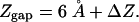
The remainder of this paper focuses on current–voltage measurements taken over individual cyclopentene molecules as a function of the tip–sample distance (Zgap). The STM control software allows for changes in the tip position (ΔZ) relative to the initial tip–sample distance (Z0) that is determined by the setpoint conditions of 0.1-nA tunneling current and –2-V sample bias. On the basis of the 10-Å value of the tip–sample spacing estimated from the current–voltage curve on the clean Si(100) surface, the measured 1-Å height of the cyclopentene molecule, and the known 5-Å actual height of cyclopentene (40), the value of Z0 when the tip is positioned over a cyclopentene molecule is estimated to be ≈6 Å. Consequently, for variable tip–sample spacing measurements on cyclopentene, we assume:
 |
[1] |
Fig. 3 shows four different current–voltage measurements taken at different values of ΔZ as specified by the STM control software. The current–voltage curves have been consecutively offset by 1 nA for clarity. From this figure, it is clear that Vpeak increases with increasing values of ΔZ. It should be noted that the sharpness of the tip (as determined by the sharpness of the cyclopentene molecules in concurrent STM images) influences the peak-to-valley ratio of the observed NDR. For example, the tip appeared less sharp during imaging for curve a in Fig. 3 compared with the other measurements. Because a tip with reduced sharpness implies a broader spatial spread of the tunneling current, the measured current–voltage curve in this case would be a superposition of resonant tunneling through the molecule and direct tunneling to the surrounding clean silicon surface. Consequently, the peak-to-valley ratio is suppressed as experimentally observed. However, because this effect is not expected to influence the value of Vpeak, variations in tip sharpness can be tolerated in these measurements. Fig. 4 is a plot of Vpeak versus ΔZ as determined from five current–voltage curves taken on individual cyclopentene molecules. Over this range of ΔZ, the apparent linearity of this plot suggests that a simple model can be used to describe the electrostatics in a semiconductor-molecule-vacuum-metal tunnel junction.
Fig. 3.

A series of four different current–voltage curves taken over isolated cyclopentene molecules at different tip–sample distances. As the tip–molecule distance increases from curve a to curve d, the peak in the current–voltage curve shifts to higher voltage. Each of the curves is offset by 1 nA for clarity.
Fig. 4.

An experimental and theoretical plot of the peak voltage (Vpeak) versus the change in tip–sample spacing (ΔZ). The theoretical curve fits the data reasonably well and allows for a quantitative estimate of the energy difference between the HOMO of the cyclopentene molecule and the Fermi level of the silicon substrate.
In general, the electrostatic potential (V) can be calculated from the Poisson equation, ▿2V = ρ/ε, where ε is the dielectric constant and ρ is the charge density, which must be determined self-consistently (41). In the limiting case where the density of states (DOS) is negligible, then the Poisson equation reduces to the Laplace equation: ▿2V = 0. This case is commonly seen for electrically insulating materials and can be represented as a capacitive equivalent circuit. On the other hand, when the DOS is large, as would be the case for a metal, then the potential profile derived from the Poisson equation is better represented as a resistive equivalent circuit. The crossover from the capacitive limit to the resistive limit occurs when the quantum capacitance exceeds the electrostatic capacitance (42).
For a molecule, the DOS between the HOMO and the lowest unoccupied molecular orbital (LUMO) is negligibly small. Consequently, when the energy window between the electrochemical potentials of the two electrical contacts in a biased molecular junction exists in the HOMO–LUMO gap, the capacitive equivalent circuit model is a reasonable approximation. For a semiconductor-molecule-vacuum-metal tunnel junction, this description holds for low biases up to the resonant tunneling condition. Consequently, a capacitive equivalent circuit model will be used to determine the theoretical dependence of Vpeak on ΔZ.
Fig. 5 schematically illustrates an isolated cyclopentene molecule bound to the Si(100)-2×1 surface that is being addressed with an idealized metal STM tip. As the simplest approximation, we assume that the molecule and the vacuum gap can each be treated as one-dimensional parallel-plate capacitors. For further simplicity, the voltage drop due to band bending at the surface is also neglected. Under these assumptions, the electrostatic potential distribution is expected to follow the sketch in Fig. 5. Although this model is almost certainly oversimplifying the underlying physics and chemistry, we will later see that it leads to a quantitative fit of the data and thus provides insight into the electrostatics of semiconductor-molecule-vacuum-metal tunnel junctions.
Fig. 5.

Schematic illustration of the silicon-molecule-vacuum-tip tunnel junction and the capacitive equivalent circuit model. During current–voltage measurements, the tip is grounded while the bias is applied to the sample. A qualitative plot of the voltage (V) versus tip–sample spacing (Z) has been inserted to illustrate the voltage drop across the molecule (Vmol) and the remaining voltage drop across the vacuum gap (Vgap). Z0 is the setpoint distance between the tip and the molecule, which is established from the STM imaging conditions in constant-current mode (tunneling current = 0.1 nA and sample bias = –2 V).
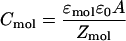
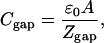
Assuming one-dimensional parallel-plate capacitors, the capacitance of the molecule (Cmol) and the capacitance of the vacuum gap (Cgap) can be written in the following forms:
 |
[2] |
and
 |
[3] |
where ε0 is the permittivity of free space, εmol is the relative permittivity of the molecule, Zmol is the height of the molecule, A is the cross-sectional area, and Zgap is the distance between the tip and molecule as defined previously in Eq. 1.
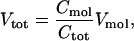
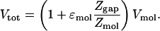
Assuming equal charge on each capacitor, the total voltage drop (Vtot) can be expressed in terms of the voltage drop across the molecule (Vmol) as
 |
[4] |
where the total capacitance (Ctot) resulting from two capacitors in series is
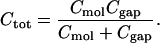 |
[5] |
Combining Eqs. 2–5 results in the following expression:
 |
[6] |
Fig. 6 is an equilibrium band diagram for this semiconductor-molecule-vacuum-metal tunnel junction. When the average voltage on the molecule (Vmol/2) matches the equilibrium potential difference (VHOMO) between the HOMO level and the semiconductor Fermi level, the resonant tunneling condition will be achieved and thus the total voltage will be equal to Vpeak. With this constraint, Eq. 6 can be rewritten in the following form:
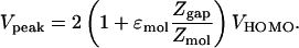 |
[7] |
Fig. 6.

An equilibrium energy band diagram of a semiconductor-molecule-vacuum-metal tunnel junction for degenerately p-type doped silicon. The potential difference between the HOMO of the cyclopentene molecule and the Fermi level of the silicon substrate is labeled as VHOMO. This parameter was quantitatively determined to be 0.74 V from the theoretical fit of Fig. 4. In this diagram, Ec is the conduction band edge, Ev is the valence band edge, EF is the Fermi level, and Evac is the vacuum energy level.
The experimentally measured values of the height and relative permittivity of cyclopentene are 5 Å and 1.26, respectively (40). Plugging these values and the expression for Zgap from Eq. 1 into Eq. 7 yields the following relationship between Vpeak (in units of volts) and ΔZ (in units of Å):
 |
[8] |
Eq. 8 was used to fit the experimental data. As seen in Fig. 4, the quality of the fit is reasonable, thus justifying the simplicity of the model over this range of ΔZ. The fitting parameter of VHOMO = 0.74 V provides an estimate of the alignment of the cyclopentene molecular orbital with the Fermi level of the substrate. Consequently, the systematic study of charge transport through a semiconductor-molecule-vacuum-metal tunnel junction as a function of tip–sample distance coupled with a capacitive equivalent circuit and resonant tunneling model provides a means for quantitatively estimating molecular orbital energies at the single-molecule level.
Conclusion
This paper has used the UHV STM for measuring charge transport through isolated cyclopentene molecules adsorbed to the degenerate p-type Si(100)-2×1 surface at a temperature of 80 K. Current–voltage measurements at 80 K show NDR at positive bias without hysteresis, which is consistent with a resonant tunneling model for a semiconductor-molecule-vacuum-metal tunnel junction. Furthermore, a series of current–voltage measurements were taken as a function of tip–sample spacing. The electrostatics of this set of experiments was treated with a capacitive equivalent circuit model, which resulted in a high-quality fit to the data. The fitting parameter in this model is the equilibrium energy difference between the HOMO of an isolated cyclopentene molecule and the Fermi level of the silicon substrate. Consequently, this combined experimental and theoretical approach allows for a quantitative estimate of molecular orbital energies at the single-molecule level. Furthermore, this model may be useful as a first approximation when attempting to engineer future silicon-based molecular electronic devices.
Acknowledgments
We thank T. Rakshit, A. W. Ghosh, and S. Datta at Purdue University for their continued collaboration and theoretical insight. We also acknowledge M. E. Greene and E. T. Foley for their assistance with the preparation of figures and the operation of the cryogenic variable temperature UHV STM, respectively. This work was supported by the National Aeronautics and Space Administration Institute for Nanoelectronics and Computing (Award NCC 2-1363), the Nanoscale Science and Engineering Initiative of the National Science Foundation (Awards EEC-0118025 and DMR-0134706), and the Defense University Research Initiative in Nanotechnology of the U.S. Army Research Office (Award DAAD 19-01-1-0521). N.P.G. acknowledges a Northwestern University Graham Fellowship.
Author contributions: N.P.G., N.L.Y., and M.C.H. designed research; N.P.G. and N.L.Y. performed research; N.P.G., N.L.Y., and M.C.H. analyzed data; and N.P.G. and M.C.H. wrote the paper.
This paper was submitted directly (Track II) to the PNAS office.
Abbreviations: UHV, ultra-high vacuum; STM, scanning tunneling microscope; NDR, negative differential resistance; HOMO, highest occupied molecular orbital.
References
- 1.Aviram, A. & Ratner, M. A. (1974) Chem. Phys. Lett. 29, 277–283. [Google Scholar]
- 2.Reed, M. A., Zhou, C., Muller, C. J., Burgin, T. P. & Tour, J. M. (1997) Science 278, 252–254. [Google Scholar]
- 3.Zhou, C., Deshpande, M. R., Reed, M. A. & Tour, J. M. (1997) Appl. Phys. Lett. 71, 611–613. [Google Scholar]
- 4.Zhou, C., Muller, C. J., Deshpande, M. R., Sleight, J. W. & Reed, M. A. (1995) Appl. Phys. Lett. 67, 1160–1162. [Google Scholar]
- 5.Chen, J., Reed, M. A., Rawlett, A. M. & Tour, J. M. (1999) Science 286, 1550–1552. [DOI] [PubMed] [Google Scholar]
- 6.Chen, J., Wang, W., Reed, M. A., Rawlett, A. M., Price, D. W. & Tour, J. M. (2000) Appl. Phys. Lett. 77, 1224–1226. [Google Scholar]
- 7.Service, R. F. (2001) Science 294, 2442–2443. [DOI] [PubMed] [Google Scholar]
- 8.Andres, R. P., Bein, T., Dorogi, M., Feng, S., Henderson, J. I., Kubiak, C. P., Mahoney, W., Osifchin, R. G. & Reifenberger, R. (1996) Science 272, 1323–1325. [DOI] [PubMed] [Google Scholar]
- 9.Metzger, R. M. (2000) J. Mater. Chem. 10, 55–62. [Google Scholar]
- 10.Collier, C. P., Mattersteig, G., Young, E. W., Luo, Y., Beverly, K., Sampaio, J., Raymo, F. M., Stoddart, J. F. & Heath, J. R. (2000) Science 289, 1172–1175. [DOI] [PubMed] [Google Scholar]
- 11.Donhauser, Z. J., Mantooth, B. A., Kelley, K. F., Bumm, L. A., Monnell, J. D., Stapleton, J. J., Price, D. W., Jr., Rawlett, A. M., Allara, D. L., Tour, J. M. & Weiss, P. S. (2001) Science 292, 2303–2307. [DOI] [PubMed] [Google Scholar]
- 12.Ramachandran, G. K., Hopson, T. J., Rawlett, A. M., Nagahara, L. A., Primak, A. & Lindsay, S. M. (2003) Science 300, 1413–1416. [DOI] [PubMed] [Google Scholar]
- 13.Park, J., Pasupathy, A. N., Goldsmith, J. I., Chang, C., Yaish, Y., Petta, J. R., Rinkoski, M., Sethna, J. P., Abruña, H. D., McEuen, P. L. & Ralph, D. C. (2002) Nature 417, 722–725. [DOI] [PubMed] [Google Scholar]
- 14.Liang, W., Shores, M. P., Bockrath, M., Long, J. R. & Park, H. (2002) Nature 417, 725–729. [DOI] [PubMed] [Google Scholar]
- 15.Nitzan, A. & Ratner, M. A. (2003) Science 300, 1384–1389. [DOI] [PubMed] [Google Scholar]
- 16.Binnig, G., Rohrer, H., Gerber, C. & Weibel, E. (1983) Phys. Rev. Lett. 50, 120–123. [Google Scholar]
- 17.Meyer, G., Bartels, L., Zophel, S., Henze, E. & Rieder, K. H. (1997) Phys. Rev. Lett. 78, 1512–1515. [Google Scholar]
- 18.Heller, E. J., Crommie, M. F., Lutz, C. P. & Eigler, D. M. (1994) Nature 369, 464–466. [Google Scholar]
- 19.Crommie, M. F., Lutz, C. P. & Eigler, D. M. (1993) Science 262, 218–220. [DOI] [PubMed] [Google Scholar]
- 20.Crommie, M. F., Lutz, C. P. & Eigler, D. M. (1993) Nature 363, 524–527. [Google Scholar]
- 21.Lyo, I. W. & Avouris, P. (1991) Science 253, 173–176. [DOI] [PubMed] [Google Scholar]
- 22.Shen, T. C., Wang, C. Abeln, G. C., Tucker, J. R., Lyding, J. W., Avouris, P. & Walkup, R. E. (1995) Science 268, 1590–1592. [DOI] [PubMed] [Google Scholar]
- 23.Foley, E. T., Kam, A. F., Lyding, J. W. & Avouris, P. (1998) Phys. Rev. Lett. 80, 1336–1339. [Google Scholar]
- 24.Hersam, M. C., Guisinger, N. P. & Lyding, J. W. (2000) Nanotechnology 11, 70–76. [Google Scholar]
- 25.Basu, R., Guisinger, N. P., Greene, M. E. & Hersam, M. C. (2004) Appl. Phys. Lett. 85, 2619–2621. [Google Scholar]
- 26.Hla, S. W., Bartels, L., Meyer, B. & Rieder, K. H. (2000) Phys. Rev. Lett. 85, 2777–2780. [DOI] [PubMed] [Google Scholar]
- 27.Stipe, B. C., Rezaei, M. A. & Ho, W. (1998) Science 280, 1732–1735. [DOI] [PubMed] [Google Scholar]
- 28.Lee, H. J. & Ho, W. (1999) Science 286, 1719–1722. [DOI] [PubMed] [Google Scholar]
- 29.Guisinger, N. P., Basu, R., Baluch, A. S. & Hersam, M. C. (2003) Ann. N.Y. Acad. Sci. 1006, 227–234. [DOI] [PubMed] [Google Scholar]
- 30.Guisinger, N. P., Basu, R., Greene, M. E., Baluch, A. S. & Hersam, M. C. (2004) Nanotechnology 15, S452–S458. [Google Scholar]
- 31.Guisinger, N. P., Greene, M. E., Basu, R., Baluch, A. S. & Hersam, M. C. (2004) Nano Lett. 4, 55–59. [Google Scholar]
- 32.Rakshit, T., Liang, G. C., Ghosh, A. W. & Datta, S. (2004) Nano Lett. 4, 1803–1807. [Google Scholar]
- 33.Foley, E. T., Yoder, N. L., Guisinger, N. P. & Hersam, M. C. (2004) Rev. Sci. Instrum. 75, 5280–5287. [Google Scholar]
- 34.Hovis, J. S., Liu, H. & Hamers, R. J. (1998) Surf. Sci. 404, 1–7. [Google Scholar]
- 35.Zhang, Z., Kulakov, M. A., Bullemer, B., Zotov, A. V. & Eisele, I. (1996) J. Vac. Sci. Technol. B 14, 2684–2689. [Google Scholar]
- 36.Kulakov, M. A., Zhang, Z., Zotov, A. V., Bullemer, B. & Eisele, I. (1996) Appl. Surf. Sci. 103, 443–449. [Google Scholar]
- 37.Komeda, T. & Nishioka, Y. (1998) Surf. Sci. 405, 38–45. [Google Scholar]
- 38.Lyo, I.-W. & Avouris, Ph. (1989) Science 245, 1369–1371. [DOI] [PubMed] [Google Scholar]
- 39.Bedrossian, P., Chen, D. M., Mortensen, K. & Golovchenko, J. A. (1989) Nature 342, 258–260. [Google Scholar]
- 40.Akiyama, R., Matsumoto, T. & Kawai, T. (2000) Phys. Rev. B 62, 2034–2038. [Google Scholar]
- 41.Datta, S., Tian, W., Hong, S., Reifenberger, R., Henderson, J. I. & Kubiak, C. P. (1997) Phys. Rev. Lett. 79, 2530–2533. [Google Scholar]
- 42.Datta, S. (2004) Nanotechnology 15, S433–S451. [Google Scholar]