Abstract
Novel van der Waals (vdW) contacts formed by layered Bi2Te3 are found effective in improving the performance of WSe2 pMOSFETs. As compared with conventional transition metal-based Ni/Au S/D contacts, over 103 times on-state current improvement is achieved. vdW interface formation between Bi2Te3 and WSe2 is confirmed by X-ray diffraction analysis and scanning transmission electron microscope observation. An atomically flat Bi2Te3/WSe2 vdW interface, where the number of defects could be reduced as small as possible, contributes to the suppression of Fermi-level pinning caused by defect-induced gap states. Moreover, the semimetal-like characteristics of Bi2Te3 are also effective in minimizing the impact of metal-induced gap states. These features offer WSe2 pMOSFETs with exceptional S/D junction characteristics, including suppressed off-state leakage and a higher on–off ratio. In addition, it is found that WSe2 pMOSFETs with Bi2Te3 S/D contacts have excellent thermal stability, maintaining device performance even after 400 °C annealing, which is very promising for CMOS back-end-of-line application. The layered tellurides, reconciling low contact resistance and high thermal stability, are promising, particularly from the perspective of their application in the manufacturing process.
Supplementary Information
The online version contains supplementary material available at 10.1038/s41598-024-79750-z.
Subject terms: Materials for devices, Materials science, Two-dimensional materials
Introduction
The device performance of transition metal dichalcogenide (TMDC) metal-oxide-semiconductor field-effect transistors (MOSFETs) has been constrained by a large contact resistance owing to severe Fermi level pinning (FLP) between metal electrodes and TMDCs1–3. The origins of FLP are usually attributed to the metal-induced gap states (MIGS) owing to metal wave function tailing into forbidden energy states4 or disorder-induced gap states (DIGS) owing to interfacial disorders/defects at metal/semiconductor interface5. For the past few decades, several approaches have been studied on TMDC for both n and pMOSFETs to alleviate FLP. Semimetal bismuth (Bi) has been shown to reduce MIGS because of its small density of states (DOS) near the Fermi level, which is very promising to enhance the device performance of MoS2 nMOSFETs6. However, the thermal stability of Bi is a major concern when considering its application to CMOS fabrication7. Besides semimetal material, van der Waals (vdW) contacts were also found effective in enhancing the device performance of MoS2 nMOSFETs as well as WSe2 pMOSFETs with metal contacts including In8, Au9, SnSe210, NiSe11, and a-GeTe12. In the meantime, the atomically flat vdW interface has a great potential to eliminate the interfacial disorders/defects between the contact material and TMDC, where the DIGS can also be suppressed. Nevertheless, the thermal stability of these kinds of contact materials are still unclear.
Recently, Sb2Te3, a famous and well-studied layered phase-change memory material13,14, has been proven as a promising S/D contact material for MoS2 nMOSFETs with low contact resistance15. Through appropriate post-metallization annealing (PMA), the well-aligned vdW Sb2Te3/MoS2 interface can be achieved by the sputtering technique. Besides, Sb2Te3 is a degenerate narrow band gap (~ 0.3 eV) semiconductor with p-type conduction, where the Fermi level of Sb2Te3 usually resides around the valence band maximum16–18. This feature allows Sb2Te3 to possess a semimetal-like characteristics. Meanwhile, since the Fermi level of Sb2Te3 is aligned near the conduction band minimum of MoS2, Sb2Te3 can reduce the contact resistance of MoS2 nMOSFETs by a mechanism of suppressing the FLP and resultant small barrier height for electrons. However, for realizing TMDC CMOS logic devices, not only MoS2 nMOSFETs but also pMOSFETs should be considered. WSe2 is a well-known p-type TMDC material, showing high intrinsic hole mobility19. Although high-performance MoS2 nMOSFETs with high-quality CVD-grown MoS2 channels have been generally demonstrated worldwide, the WSe2 pMOSFETs with comparable performance to the MoS2 nMOSFETs are still beset with difficulties20–22, owing to unstable monolayer channel quality23, ambipolar transport behavior24 and large contact resistance22.
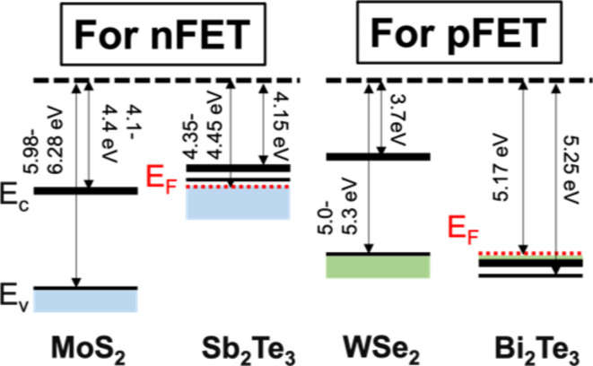
Searching for a similar Te-based material but with high electron affinity/work function for WSe2 pMOSFETs application, we found Bi2Te3 is a promising candidate. Bi2Te3 shows the similar crystal structure as Sb2Te3 with slightly different lattice constants. Nevertheless, Bi2Te3 exhibits a tendency to become a degenerate n-type semiconductor, where its Fermi-level locates near the conduction band minimum25. Figure 1 shows the comparison of band alignment of Sb2Te3 with MoS2 and Bi2Te3 with WSe2 as depicted using the theoretical/experimental band parameters25–29. As mentioned and already demonstrated, judging from the band alignment, Sb2Te3 is suitable for MoS2 nMOSFETs, while Bi2Te3 has a potential being compatible for WSe2 pMOSFETs.
Fig. 1.
The band alignment of Sb2Te3/MoS2 and Bi2Te3/WSe2, indicating the Te-based contacts are suitable for fabricating MoS2 nMOSFETs and WSe2 pMOSFETs. The figure is remodified from Fig. 5a in Ref. 15.
In this work, monolayer (1L) WSe2 pMOSFETs with Bi2Te3 S/D contacts were fabricated and subjected to PMA at different temperatures to verify the feasibility of Bi2Te3 as a contact material and to investigate its thermal stability. The Bi2Te3/WSe2 can also form a well-aligned vdW interface under appropriate thermal treatment, just like that of Sb2Te3 on MoS2. It is worth noting that significant device performance enhancement of the WSe2 pMOSFET with Bi2Te3 S/D contacts was observed as compared with the controlled device using the Ni/Au contacts, indicating the possibility of contact resistance reduction at the Bi2Te3/WSe2 interface. Most important of all, the S/D contact characteristics and device performance can maintain or even improve after 400 °C PMA, suggesting the high thermal stability of Bi2Te3 and the feasibility of applying it to CMOS fabrication.
Results and discussion
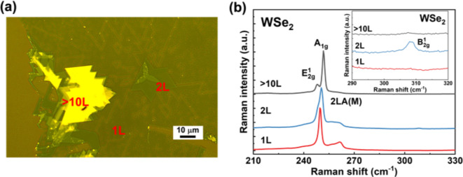
Figure 2a is the top view of optical microscope (OM) image of CVD-grown WSe2 flakes, where the WSe2 flakes consist of WSe2 with different thickness including 1L, two-layer (2L) and bulk region with layer numbers over 10L. The comparison of Raman spectra of WSe2 with different thicknesses is shown in Fig. 2b. It is found that the distribution of Raman peaks is very sensitive to WSe2 thickness and can be used as a fingerprint for WSe2 with different layer numbers. For WSe2 with multi-layers over 10L, obvious  (248. 1 cm−1) mode and A1g mode (251.8 cm−1) peaks were observed, which agrees with the spectra extracted from a WSe2 bulk crystal30. On the other hand, for few-layer WSe2, the
  mode and A1g mode merged or degenerated into a single peak and 2LA(M) mode near 261.2 cm−1 resulting from the second-order Raman mode owing to two-phonon scattering at the M point of the Brillouin zone31,32 appeared. Besides, as compared with multi-layer WSe2 (the inset of Fig. 2b), the absence of
  peak at around 308.5 cm−1 is a signature to confirm the monolayer thickness of the WSe2 channel30,33.
Fig. 2.
(a) The optical microscope (OM) image of the top view of CVD-grown WSe2 with different thicknesses. The scale bar is 10 μm. (b) The comparison of Raman spectra of WSe2 with different thicknesses. The fingerprint of Raman peaks is very sensitive to WSe2 thickness. The inset shows WSe2 Raman spectra focusing on Raman shift from 290 to 320 cm−1.
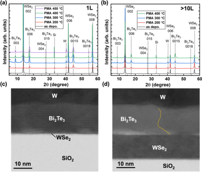
The WSe2 samples used for X-ray diffraction (XRD) analysis can be separated into two kinds. One mainly consists of 1L WSe2 with small portion (< 10%) of multi-layer WSe2, which will be referred to as 1L WSe2 afterward. The other mainly consists of multi-layer WSe2 with layer numbers over 10L, which will be referred to as > 10L WSe2 afterward. Figure 3a,b shows the XRD θ/2θ scan of W/Bi2Te3/WSe2/SiO2/Si stacked films before and after PMA at temperatures from 200 to 450 °C extracted from 1L WSe2 and > 10L WSe2 samples. For the as-deposited sample, a small peak of Bi2Te3 015 can be found at around 2θ = 28°. This is the strongest peak observed for the powder sample34, indicating the as-deposited Bi2Te3 film consists of randomly oriented polycrystalline with tiny grain size. The Bragg reflections of the crystalline Bi2Te3 (001) plane emerged after 200 °C PMA and became much stronger after 400 °C PMA, indicating that the Bi2Te3 crystal grains changed the orientation from random to c-axis oriented through thermal treatment. Note that highly c-axis oriented Bi2Te3 and WSe2 peaks were still present even after 400 °C PMA, suggesting that the layer structure of Bi2Te3 film and the well-aligned Bi2Te3/WSe2 interface preserved. This behavior of thermal-induced crystallization of Bi2Te3 on WSe2 is very similar to that of Sb2Te3/MoS2 case15. However, further annealing at 450 °C resulted in a decrease of the peak intensity for both Bi2Te3 and WSe2 peaks, indicating the degradation of the interfacial quality of the heterostructure. From a materials point of view, the Bi2Te3/WSe2 heterostructure can sustain at least 400 °C annealing, which meets the thermal budget requirement of back-end-of-line (BEOL) for CMOS fabrication. Moreover, the peak intensity of Bi2Te3 006 and 0015 peaks is much stronger for Bi2Te3 on 1L WSe2 (Fig. 3a) as compared with those on > 10L WSe2 (Fig. 3b), suggesting Bi2Te3 has better crystallinity on 1L WSe2. This phenomenon was also confirmed in the STEM cross-sectional images as shown in Fig. 3c,d for W/Bi2Te3 stacked film deposited on 1L WSe2 and > 10L WSe2 after 400 °C annealing. For W/Bi2Te3 on 1L WSe2 (Fig. 3c), a well-aligned layered structure of Bi2Te3 is clearly observed without any in-plane grain boundaries and distinct defects at this scale. Conversely, a clear grain boundary (yellow dashed line) was observed for those on > 10L WSe2 (Fig. 3d). It is found that SeOx on the surface of > 10L WSe2 hinders the atomic alignment between Bi2Te3 and WSe2. Moreover, some grains do not show c-axis orientation as indicated by absence of lattice fringes parallel to the substrate surface. Since selenium (Se) has very low chemical reactivity and the selenization of WO3 only happens at certain growth condition, the Se may tend to pile up on > 10L WSe2 during CVD growth owing to incomplete reaction35. The Se residues will then lead to SeOx formation after air exposure.
Fig. 3.
XRD θ/2θ scan of W/Bi2Te3/WSe2/SiO2/Si stacked films before and after PMA from 200 to 450 °C extracted from (a) 1L WSe2 and (b) > 10L WSe2. The high-resolution scanning transmission electron microscope (STEM) cross-sectional images of 400 °C annealed W/Bi2Te3 stacked film as deposited on (c) 1L WSe2 and (d) > 10L WSe2. The yellow dashed line indicates the boundary between polycrystalline Bi2Te3 with tiny grain size and layered Bi2Te3.
A detailed energy dispersive X-ray (EDX) mapping analysis of the Fig. 3d is presented. (see Supplementary Fig. S1). In addition, surface roughness for thick WSe2 film may affect the growth behavior of Bi2Te3 film. This evidence indicates that the surface cleanness as well as flatness of WSe2 are key factors for transferring poly crystalline Bi2Te3 into a highly oriented structure during thermal treatment.
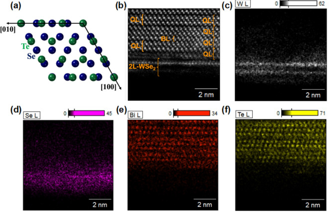
Figure 4a shows the smallest repeating cell of the Bi2Te3/WSe2 vdW interface viewed from the [001] (c-axis) direction based on the lattice information, where Bi2Te3 possesses lattice constants of a = b = 4.388 Å and c = 30.46 Å36, and those of WSe2 are a = b = 3.288 Å and c = 12.989 Å37. Note that since both materials adopt hexagonal symmetry, the deposited Bi2Te3 could follow the atomic alignment of underlayer WSe2, where the atomic positions of terminated Te and Se nearly match every three and four unit cells, respectively, along the in-plane direction. Moreover, thanks to the layered nature of Bi2Te3, the large in-plane lattice mismatch does not influence the growth on WSe2, which is known as the vdW epitaxy38. Figure 4b shows the High-Angle Annular Dark Field (HAADF)-STEM images focusing on the interface between Bi2Te3 and WSe2, where Bi2Te3 is also fabricated by sputtering as mentioned in Fig. 3, and Fig. 4c–f correspond to the EDX mapping analysis of W, Se, Bi, and Te. The heterostructure is subjected to a 400 °C annealing process. Note that as can be seen in Fig. 4c, the elemental mapping of W exhibits two lateral lines, indicating the observed area contains bilayer WSe2. Nevertheless, the discussion regarding the interfacial stability is still valid for Bi2Te3/2L-WSe2 heterostructure. A vdW interface composed of Bi2Te3 quintuple layer (QL) (Te-Bi-Te-Bi-Te stacking) and WSe2 monolayer (Se-W-Se stacking) is clearly visible. It was found that the Bi2Te3 layer contains not only QLs but the bilayer (BL) can be also seen (Fig. 4b).
Fig. 4.
(a) A top-view illustration of the smallest repeating cell of the Bi2Te3/WSe2 vdW interface. To prevent complexity, only Te and Se atoms adjacent to a vdW gap are shown. (b) The enlarged HAADF-STEM images of the Bi2Te3/WSe2 interface, indicating the formation of the vdW interface. The EDX mapping of (c) W, (d) Se, (e) Bi, and (f) Te at the Bi2Te3/WSe2 interface, suggesting no chemical interaction occurs.
The same BL stacking fault, known as bilayer swapping, was reported for Sb2Te3, but the electrical properties such as carrier concentration are not largely influenced by the presence of BL39,40. According to the EDX mapping, neither interfacial mixing nor interdiffusion is observed at the Bi2Te3/WSe2 interface, indicating that the vdW interface can be maintained even after 400 °C annealing. We believe that the almost defect-free and highly stable vdW interface could provide the Fermi-level unpinning at the Bi2Te3/WSe2 interface, which helps to enhance the device performance of the WSe2 device.
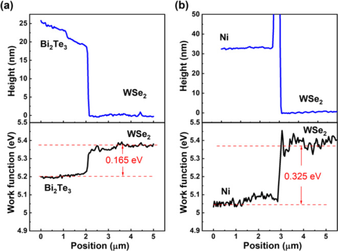
Figure 5 shows the typical height and average work function (WF) profile of the Bi2Te3/WSe2 and Ni/WSe2 interface extracted by Kelvin Probe Force Microscopy (KPFM), respectively. Since the electrodes on WSe2 were fabricated through lift-off process, the abrupt edge between electrodes and WSe2 is hard to obtain owing to the photoresist residue. We define the averaged CPD of WSe2 away from the interface about 1 μm. The averaged WF value of WSe2 of 5.37 eV was derived through the CPD difference from Au (5.47 eV)41 reference pad on WSe2. The corresponding optical images and KPFM CPD images are also presented (see Supplementary Fig. S2). The WF of Bi2Te3 and Ni were then determined to be 5.21 and 5.02 eV, respectively. The obtained WF value of WSe2 and Bi2Te3 are all very close to the theoretical value as depicted in Fig. 1. Moreover, a lower Fermi-level difference is expected for Bi2Te3/WSe2 than that of Ni on WSe2. If the Fermi-level is unpinned, Bi2Te3 has a great potential to achieve better p-type transport properties on WSe2.
Fig. 5.
Height profile and corresponding averaged work function profile of the (a) Bi2Te3/WSe2 and (b) Ni/WSe2 interface.
To investigate the electrical properties of Bi2Te3 on WSe2 as a contact material, we fabricated the back gate 1L WSe2 pMOSFETs with Bi2Te3 contact. Figure 6a is the detailed process flow and a schematic cross-sectional figure of a 1L WSe2 pMOSFET with Bi2Te3 S/D contacts. Figure 6b shows the Raman spectrum obtained from the channel region between the S/D metal pads of WSe2 pMOSFET, as shown in the inset, where the electrode gap size is around 5 μm. The peak position shift between  mode and A1g mode and the absence of
  peak is in good agreement with 1L WSe2, as mentioned in Fig. 2.
Fig. 6.
(a) The detailed process flow and a schematic cross-sectional figure of a 1L WSe2 pMOSFET with Bi2Te3 contacts and Au back-gate. (b) 1L WSe2 Raman spectrum obtained from the channel region between the S/D metal pads. The inset shows the OM image of a top view of the back-gate 1L WSe2 pMOSFET.
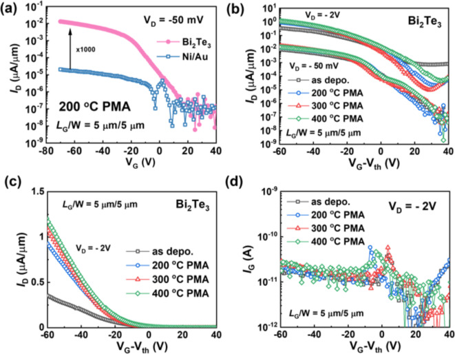
Figure 7a compares the ID–VG transfer curves extracted from the 1L WSe2 pMOSFETs with Bi2Te3 and Ni/Au S/D contacts. For a fair comparison, all the devices were subjected to PMA at 200 °C for 10 min. The 5-µm-gate-length WSe2 pMOSFETs with Bi2Te3/W contacts exhibited significant device performance enhancement as compared with those of Ni/Au control devices. A high on–off ratio of ∼106 was obtained at a VD of -50 mV. Moreover, the on-state current (Ion) of the devices with Bi2Te3/W contacts considerably increases to approximately 103 times greater than that of the MOSFETs using Ni/Au for S/D contacts. These results suggest a significant contact resistance reduction by employing Bi2Te3 contacts, which can be attributed to the low Fermi-level difference between Bi2Te3 and WSe2 (Fig. 5). Due to the semi-metallic characteristics of Bi2Te3 for suppressing MIGS and vdW interface for suppressing DIGS, the Fermi-level between Bi2Te3 and WSe2 tends to unpin, so the small Fermi-level difference can be maintained and leads to better device performance. Besides Ni/Au S/D contacts, we also compare Bi2Te3 contacts with Cr/Au contact (see Supplementary Fig. S3). Significant device performance enhancement was also observed, suggesting the effectiveness of Bi2Te3 contacts for improving junction characteristics on WSe2. The thermal stability of 1L WSe2 pMOSFETs was also investigated. Figure 7b shows the comparison of ID-VG transfer curves at VD of -50 mV and -2 V for 1L WSe2 pMOSFETs with Bi2Te3/W contacts before and after the PMA process at different temperatures. Reduced off-state leakage (Ioff) and enlarged on–off ratio with increasing PMA temperature are visible, indicating the S/D junction characteristics improvement through thermal treatment. At VD of − 2 V, increasing Ion is observed with increasing PMA temperature, which is more obvious in the linear scale as shown in Fig. 7c. This indicates the contact resistance reduction and the high thermal stability of Bi2Te3/WSe2 contacts. Approximately 3 times Ion enhancement was achieved after 400 °C PMA as compared with its as-deposited counterpart, suggesting the benefits of vdW interface formation for reducing contact resistance. The Ion enhancement mainly resulted from the contact resistance reduction instead of gate leakage current (IG), as IG remains considerably low during the thermal treatment, as shown in the Fig. 7d.
Fig. 7.
(a) Comparison of ID-VG transfer curves of devices with Bi2Te3/W and Ni/Au S/D contacts on 285-nm-thick SiO2 dielectrics. (b) Comparison of ID-VG transfer curves of devices with Bi2Te3/W contacts before and after the PMA process at different temperatures. (c) The linear scale of ID-VG transfer curves shown in Fig. 6b. (d) The comparison of IG of devices with Bi2Te3/W contacts before and after the PMA process at different temperatures.
Nevertheless, kinks at the subthreshold region were visible after thermal treatment and got worse at 400 °C. Since the WSe2 of our devices is not covered by any protection layer, this phenomenon may be attributed to the interfacial degradation between WSe2 and backside SiO2 and the damage of WSe2 itself.
Conclusion
Thermally stable Bi2Te3/WSe2 vdW contact up to 400 °C was fabricated, and significant device performance improvement was realized owing to the atomic-level defect-free vdW interface. The Bi2Te3/WSe2 heterostructure can go through and maintain its quality at least after 400 °C annealing, which fulfills the requirement for the BEOL CMOS process. Moreover, significant enhancement of device performance in terms of up to 103 times current improvement was demonstrated using Bi2Te3/WSe2 contacts as compared with conventional transition metal contacts. This also indicates significant contact resistance reduction. All evidence shown in this work supports that layered tellurides can be applied to not only MoS2 nMOSFETs but also WSe2 pMOSFETs as S/D contacts, which is very promising for TMDC CMOS applications.
Methods
Synthesis of WSe2
By using chemical vapor deposition (CVD), WSe2 flakes were deposited on SiO2 (285 nm)/Si substrates at 880 °C with WO3 powder, Se beads, and KBr powder42,43. KBr powder was used as the growth promoter44.
Bi2Te3 deposition by sputtering
To investigate the crystal quality of Bi2Te3 on WSe2 and its applicability to contact material, 20-nm-thick Bi2Te3 and 30-nm-thick tungsten (W) films were deposited onto the WSe2 by magnetron sputtering at room temperature (300 K) (QAM-4, ULVAC KYUSYU Corp.)14,45. W was treated as a protection layer for Bi2Te3 during the thermal treatment.
Material characterization
Raman analysis was used to determine the thickness of the WSe2 layer. The Raman spectra were extracted from the HORIBA LabRAM Raman spectrometer with 488 nm wavelength laser excitation using a power of 5 mW. X-ray diffraction (XRD) and scanning transmission electron microscope (STEM) were used to investigate the crystallinity of Bi2Te3 and the Bi2Te3/WSe2 interface. For XRD analysis, Cu-Ka (l = 1.542 Å) was used in a Bragg–Brentano geometry (Ultima IV, Rigaku Corp.). A focused ion beam (FIB) technique was used to prepare the STEM sample, and JEM-ARM200F (JEOL, Ltd.) was used to study the cross-sectional images of Bi2Te3 and WSe2 and energy dispersive X-ray (EDX) mapping with an accelerating voltage of 200 kV was performed. Kelvin probe force microscopy (KPFM) was used to measure the contact potential difference (CPD), which can be used to extract the work function difference between metal electrodes and WSe2. A standard atomic force microscope (Park Systems NX10) was utilized with a conductive cantilever (Olympus AC240TM, Pt coat) for CPD measurement under ambient condition.
Fabrication of back gate 1L WSe2 MOSFETs
After WSe2 growth, photolithography was used for defining S/D regions. 20-nm-thick Bi2Te3 and 30-nm-thick W films were then deposited onto the WSe2 layer by magnetron sputtering. The S/D contacts were then fabricated through a lift-off process using acetone and isopropanol (IPA) at 25 °C. Subsequently, the backside SiO2 of the samples was removed using hydrogen fluoride (HF) solution, followed by back-gate Au deposition using sputtering. Post metallization annealing (PMA) was performed in Ar ambient for 10 min at 200, 300 and 400 °C. The back-gate devices with Ni (50 nm)/Au (50 nm) S/D metal contacts were also fabricated for comparison. Ni and Au were deposited by e-beam evaporator, respectively. To eliminate the impact from WSe2 quality and WSe2/SiO2 interfacial condition on device performance, we fabricated the devices with different S/D metal contacts on the same WSe2 sample grown by CVD.
Electrical characterization
All electrical characterization of WSe2 MOSFETs was performed in a standard probe station under atmospheric condition at room temperature, and Keysight B1500A was used for electrical measurements.
Electronic supplementary material
Below is the link to the electronic supplementary material.
Acknowledgements
This work is supported by JST-MIRAI (JPMJMI22708192), JST FOREST Program (JPMJFR213X), JST-CREST (JPMJCR23A4), NICT (05901), and Kakenhi Grants-in-Aid (JP21H05232, JP21H05234, JP22H04957) from the Japan Society for the Promotion of Science (JSPS).
Author contributions
T. I. supervised the overall project. T. I., W. H. C., and N. O. planned and conceived the research and experiment. S. H. and Y. S. contributed to the Bi2Te3 deposition and XRD analysis. T. E. and Y. M. contributed to the WSe2 CVD growth. W. H. C. contributed to the device fabrication, electrical properties measurement, KPFM measurement and data analysis. The manuscript was written by W. H. C., S. H., Y. S., and T. I. with discussion and inputs from all authors.
Data availability
The datasets used and/or analyzed during the current study available from the corresponing author on reasonable request.
Competing interests
The authors declare no competing interests.
Footnotes
Publisher’s note
Springer Nature remains neutral with regard to jurisdictional claims in published maps and institutional affiliations.
Contributor Information
Wen Hsin Chang, Email: wh-chang@aist.go.jp.
Yuta Saito, Email: yuta.saito.e5@tohoku.ac.jp.
References
- 1.Bampoulis, P. et al. Defect dominated charge transport and fermi level pinning in MoS2/metal contacts. ACS Appl. Mater. Inter.9, 19278–19286. 10.1021/acsami.7b02739 (2017). [DOI] [PMC free article] [PubMed] [Google Scholar]
- 2.Sotthewes, K. et al. Universal fermi-level pinning in transition-metal dichalcogenides. J. Phys. Chem. C123, 5411–5420. 10.1021/acs.jpcc.8b10971 (2019). [DOI] [PMC free article] [PubMed] [Google Scholar]
- 3.Liu, X., Choi, M. S., Hwang, E., Yoo, W. J. & Sun, J. Fermi level pinning dependent 2D semiconductor devices: Challenges and prospects. Adv. Mater.34, 2108425. 10.1002/adma.202108425 (2022). [DOI] [PubMed] [Google Scholar]
- 4.Mönch, W. Chemical trends of barrier heights in metal-semiconductor contacts: On the theory of the slope parameter. Appl. Sur. Sci.92, 367–371. 10.1016/0169-4332(95)00257-X (1996). [Google Scholar]
- 5.Hasegawa, H. & Ohno, H. Unified disorder induced gap state model for insulator-semiconductor and metal-semiconductor interfaces. J. Vac. Sci. Technol. B4, 1130–1138. 10.1116/1.583556 (1986). [Google Scholar]
- 6.Shen, P. C. et al. Ultralow contact resistance between semimetal and monolayer semiconductors. Nature593, 211–217. 10.1038/s41586-021-03472-9 (2021). [DOI] [PubMed] [Google Scholar]
- 7.Chou, A. S. et al. Antimony semimetal contact with enhanced thermal stability for high performance 2D electronics. IEEE Int. Electron Device Meet. 150–153. 10.1109/IEDM19574.2021.9720608 (2021). [Google Scholar]
- 8.Wang, Y. et al. Van der Waals contacts between three-dimensional metals and two-dimensional semiconductors. Nature568, 70–74. 10.1038/s41586-019-1052-3 (2019). [DOI] [PubMed] [Google Scholar]
- 9.Kwon, G. et al. Interaction- and defect-free van der Waals contacts between metals and two-dimensional semiconductors. Nat. Electron.5, 241–247. 10.1038/s41928-022-00746-6 (2022). [Google Scholar]
- 10.Jang, J. et al. Fermi-level pinning-free WSe2 transistors via 2D Van der Waals metal contacts and their circuits. Adv. Mater.34, 2109899. 10.1002/adma.202109899 (2022). [DOI] [PubMed] [Google Scholar]
- 11.Zhao, B. et al. Van der Waals epitaxial growth of ultrathin metallic NiSe nanosheets on WSe2 as high performance contacts for WSe2 transistors. Nano Res.12, 1683–1689. 10.1007/s12274-019-2423-7 (2019). [Google Scholar]
- 12.Li, W. et al. Synthesis of 2D α-GeTe single crystals and α-GeTe/WSe2 heterostructures with enhanced electronic performance. Adv. Funct. Mater.32, 2201673. 10.1002/adfm.202201673 (2022).37521161 [Google Scholar]
- 13.Noé, P., Vallée, C., Hippert, F., Fillot, F. & Raty, J.-Y. Phase-change materials for non-volatile memory devices: From technological challenges to materials science issues. Semicond. Sci. Technol.33, 013002. 10.1088/1361-6641/aa7c25 (2018). [Google Scholar]
- 14.Saito, Y. et al. Recent developments concerning the sputter growth of chalcogenide-based layered phase-change materials. Mater. Sci. Semicond. Process135, 106079. 10.1016/j.mssp.2021.106079 (2021). [Google Scholar]
- 15.Chang, W. H. et al. Sb2Te3/MoS2 Van der Waals junctions with high thermal stability and low contact resistance. Adv. Electron. Mater.9, 2201091. 10.1002/aelm.202201091 (2023). [Google Scholar]
- 16.Kulbachinskii, V. A. et al. Valence-band changes in Sb2-xInxTe3 and Sb2Te3-ySey by transport and Shubnikov-de Haas effect measurements. Phys. Rev. B52, 10915–10922. 10.1103/physrevb.52.10915 (1995). [DOI] [PubMed] [Google Scholar]
- 17.Horak, J., Drasar, C., Novotny, R., Karamazov, S. & Lostak, P. Non-stoichiometry of the crystal lattice of antimony telluride. Phys. Status Solidi A149, 549–556. 10.1002/pssa.2211490205 (1995). [Google Scholar]
- 18.Ko, D. K., Kang, Y. & Murray, C. B. Enhanced thermopower via carrier energy filtering in solution-processable Pt-Sb2Te3 nanocomposites. Nano Lett.11, 2841–2844. 10.1021/nl2012246 (2011). [DOI] [PubMed] [Google Scholar]
- 19.Movva, H. C. P. et al. High-mobility holes in dual-gated WSe2 field-effect transistors. ACS Nano9, 10402–10410. 10.1021/acsnano.5b04611 (2015). [DOI] [PubMed] [Google Scholar]
- 20.Maxey, K. et al. 300 mm MOCVD 2D CMOS materials for more (Than) moore scaling. Symp. VLSI Technol. 419–420. 10.1109/VLSITechnologyandCir46769.2022.9830457 (2022). [Google Scholar]
- 21.Hung, T. Y. T. et al. pMOSFET with CVD-grown 2D semiconductor channel enabled by ultra-thin and fab-compatible spacer doping. IEEE Int. Electron. Device Meet. 150–153. 10.1109/IEDM45625.2022.10019321 (2022). [Google Scholar]
- 22.O’Brn, K. P. et al. Advancing 2D monolayer CMOS through contact channel and interface engineering. IEEE Int. Electron. Device Meet. 146–149. 10.1109/IEDM19574.2021.9720651 (2021). [Google Scholar]
- 23.Choi, S. H. et al. Is chemical vapor deposition of monolayer WSe2 comparable to other synthetic routes? APL Mater.11, 111124. 10.1063/5.0175469 (2023). [Google Scholar]
- 24.Wang, X. et al. High-performance n-type transistors based on CVD-grown large-domain trilayer WSe2. APL Mater.9, 071109. 10.1063/5.0048983 (2021). [Google Scholar]
- 25.Liu, D. et al. Anisotropic layered Bi2Te3-In2Te3 composites: Control of interface density for tuning of thermoelectric properties. Sci. Rep.7, 43611. 10.1038/srep43611 (2017). [DOI] [PMC free article] [PubMed] [Google Scholar]
- 26.Zhang, Z., Zhang, H., Wu, Y., Zeng, Z. & Hu, Z. Optimization of the thermopower of antimony telluride thin film by introducing tellurium nanoparticles. Appl. Phys. A118, 1043–1051. 10.1007/s00339-014-8871-8 (2014). [Google Scholar]
- 27.Guo, Y. H., Wang, Z. F., Zhang, L. Z., Shen, X. D. & Liu, F. Thickness dependence of surface energy and contact angle of water droplets on ultrathin MoS2 films. Phys. Chem. Chem. Phys.18, 14449–14453. 10.1039/C6CP00036C (2016). [DOI] [PubMed] [Google Scholar]
- 28.Kang, J., Tongay, S., Zhou, J., Li, J. & Wu, J. Band offsets and heterostructures of two-dimensional semiconductors. Appl. Phys. Lett.102, 012111. 10.1063/1.4774090 (2013). [Google Scholar]
- 29.Liu, W. et al. Role of metal contacts in designing high-performance monolayer n-type WSe2 field effect transistors. Nano Lett.13, 1983–1990. 10.1021/nl304777e (2013). [DOI] [PubMed] [Google Scholar]
- 30.Tonndorf, P. et al. Photoluminescence emission and Raman response of monolayer MoS2, MoSe2, and WSe2. Opt. Express21, 4908–4916. 10.1364/OE.21.004908 (2013). [DOI] [PubMed] [Google Scholar]
- 31.Sourisseau, C., Cruege, F. & Fouassier, M. Second-order Raman effects, inelastic neutron scattering and lattice dynamics in 2H-WS2. Chem. Phys.150, 281–293. 10.1016/0301-0104(91)80136-6 (1991). [Google Scholar]
- 32.Molina-Sánchez, A. & Wirtz, L. Phonons in single-layer and few-layer MoS2 and WS2. Phys. Rev. B84, 155413. 10.1103/PhysRevB.84.155413 (2011). [Google Scholar]
- 33.Terrones, H. et al. New first order Raman-active modes in few layered transition metal dichalcogenides. Sci. Rep.4, 4215. 10.1038/srep04215 (2014). [DOI] [PMC free article] [PubMed] [Google Scholar]
- 34.Xu, J.-L. et al. Ultrasensitive nonlinear absorption response of large-size topological insulator and application in low-threshold bulk pulsed lasers. Sci. Rep.5, 14856. 10.1038/srep14856 (2015). [DOI] [PMC free article] [PubMed] [Google Scholar]
- 35.Yao, Z., Liu, J., Xu, K., Chow, E. K. C. & Zhu, W. Material synthesis and device aspects of monolayer tungsten diselenide. Sci. Rep.8, 5221. 10.1038/s41598-018-23501-4 (2018). [DOI] [PMC free article] [PubMed] [Google Scholar]
- 36.α-Bi2Te3 (Bi2Te3) Crystal Structure: Datasheet from “PAULING FILE Multinaries Edition-2022” in SpringerMaterials (https://materials.springer.com/isp/crystallographic/docs/sd0543893).
- 37.2H-WSe2 (WSe2 rt 2H) Crystal Structure: Datasheet from “PAULING FILE Multinaries Edition-2022” in SpringerMaterials (https://materials.springer.com/isp/crystallographic/docs/sd0310430).
- 38.Koma, A. Van der Waals epitaxy—A new epitaxial growth method for a highly lattice-mismatched system. Thin Solid Films216, 72–76. 10.1016/0040-6090(92)90872-9 (1992). [Google Scholar]
- 39.Wang, J.-J. et al. Layer-switching mechanisms in Sb2Te3. Phys. Stat. Sol. (RRL)13, 1900320. 10.1002/pssr.201900320 (2019). [Google Scholar]
- 40.Wang, J. et al. Enhancing thermoelectric performance of Sb2Te3 through swapped bilayer defects. Nano Energy79, 105484. 10.1016/j.nanoen.2020.105484 (2021). [Google Scholar]
- 41.Yoshitake, M. & Yagyu, S. Work function for applications—How work function is determined, modified and applied for band alignment. IEEJ Trans. EIS129, 1169–1175. 10.1541/ieejeiss.129.1169 (2009). [Google Scholar]
- 42.Irisawa, T. et al. CVD grown bilayer WSe2/MoSe2 heterostructures for high performance tunnel transistors. Jpn. J. Appl. Phys.59, SGGH05. 10.7567/1347-4065/ab650d (2020). [Google Scholar]
- 43.Wada, N. et al. Efficient and chiral electroluminescence from in-plane heterostructure of transition metal dichalcogenide monolayers. Adv. Funct. Mater.32, 2203602. 10.1002/adfm.202203602 (2022). [Google Scholar]
- 44.Li, S. et al. Halide-assisted atmospheric pressure growth of large WSe2 and WS2 monolayer crystals. Appl. Mater. Today1, 60–66. 10.1016/j.apmt.2015.09.001 (2015). [Google Scholar]
- 45.Saito, Y. et al. Compositional tuning in sputter-grown highly-oriented Bi–Te films and their optical and electronic stuctures. Nanoscale9, 15115–15121. 10.1039/C7NR04709F (2017). [DOI] [PubMed] [Google Scholar]
Associated Data
This section collects any data citations, data availability statements, or supplementary materials included in this article.
Supplementary Materials
Data Availability Statement
The datasets used and/or analyzed during the current study available from the corresponing author on reasonable request.


