

Abstract
Despite decades of extensive research on thermoelectric materials, Bi2Te3 alloys have dominated room-temperature applications. However, recent advancements have highlighted the potential of alternative candidates, notably Mg3Sb2–Mg3Bi2 alloys, for low- to mid-temperature ranges. This study optimizes the low-temperature composition of this alloy system through Nb addition (Mg3.2–xNbx(Sb0.3Bi0.7)1.996Te0.004), characterizing composition, microstructure, and transport properties. A high Mg3Bi2 content improves the band structure by increasing weighted mobility while enhancing the microstructure. Crucially, it suppresses detrimental grain boundary scattering effects for room-temperature applications. While grain boundary scattering suppression is typically achieved through grain growth, our study reveals that Nb addition significantly reduces grain boundary resistance without increasing grain size. This phenomenon is attributed to a grain boundary complexion transition, where Nb addition transforms the highly resistive Mg3Bi2-rich boundary complexion into a less resistive, metal-like interfacial phase. This marks the rare demonstration of chemistry noticeably affecting grain boundary interfacial electrical resistance in Mg3Sb2–Mg3Bi2. The results culminate in a remarkable advancement in zT, reaching 1.14 at 330 K. The device ZT is found to be 1.03 at 350 K, which further increases to 1.24 at 523 K and reaches a theoretical maximum device efficiency (ηmax) of 10.5% at 623 K, underscoring its competitive performance. These findings showcase the outstanding low-temperature performance of n-type Mg3Bi2–Mg3Sb2 alloys, rivaling Bi2Te3, and emphasize the critical need for continued exploration of complexion phase engineering to advance thermoelectric materials further.
Keywords: thermoelectric; Mg3(Sb, Bi)2; niobium; grain boundary complexion; two-phase model
1. Introduction
Concerns on environmental pollution, global warming, and greenhouse gas emissions have been increasing over the last decades. Therefore, many countries have agreed on the net zero emission, climate policy and integration of green energy systems by 2050.1 Considering more than half of the energy is lost as waste heat by industry, transportation, or everyday activities, harvesting waste heat for alternative energy presents a compelling solution, significantly mitigating greenhouse gas emissions and curbing overall energy consumption with notable efficiency. The thermoelectric effect relies on converting the temperature gradient effectively to electricity and vice versa. Compared to high-quality waste heat (above 573 K), recovering low-grade waste heat, which makes up to ca. 90% of the source, is challenging due to its lower energy density.2−4 So far, the thermoelectric cooling market has been essentially dominated by Bi2Te3-based materials.5 However, the diminishing availability and toxicity of the Te element are reducing the practicality of Bi2Te3, prompting a shift in focus toward alternative materials.6 While the majority of thermoelectric studies have concentrated on materials with high thermoelectric figure-of-merit, zT values (zT = S2σT/κ, where S is the Seebeck coefficient, σ is electrical conductivity, T is the absolute temperature, and κ is thermal conductivity) in mid- and high-temperature ranges, such as lead chalcogenides,7−9 skutterudites,10−13 and half-Heuslers,14−16 there has been a recent surge in interest in Mg3Sb2 and Mg3Bi2-based materials. These alternatives are gaining attention for both low and mid-temperature applications, providing a potential substitute for Bi2Te3 materials. Indeed, recent studies have showcased impressive thermoelectric performances achieved through Mg3Sb2 and Mg3Bi2-based thermoelectric materials and modules.2−4,17−22
Mg3Sb2 is known as a great candidate for thermoelectric applications due to the characteristic properties obeying the phonon-glass electron-crystal concept, displaying inherently low κ along with favorable electronic transport behavior.23−25 To date, various strategies have been applied to enhance the thermoelectric efficiency of the Mg3Bi2 system, such as microstructure engineering, carrier concentration optimization, band structure modification, annealing, etc.4,19,21,25−33 Among these studies, alloying with Mg3Bi2 has notably enhanced the zT which has been attributed to an improved band structure (higher weighted mobility) and modifying scattering mechanisms.4,19,22,34−39
Despite their potential, the room temperature thermoelectric properties of Mg3Sb2- and Mg3Bi2-based thermoelectric materials are known to be severely limited due to grain boundary electrical resistance. Originally thought to be due to ionized impurity scattering36 that could be modified by incorporation of other elements such as Nb; it was discovered that a thermally activated grain boundary electrical resistance leads to low σ and, therefore, low zT at room temperature.31,40,41 Luo et al.33 through experimental techniques including nuclear magnetic resonance (NMR), atom probe tomography (APT), and scanning/transmission electron microscopy (SEM/TEM), along with theoretical work by Gorai et al.42 demonstrated that Nb does not significantly diffuse into the Mg3Sb2 crystal structure and thus could not alter the doping or scattering in Mg3Sb2 but instead was clearly present in and near the grain boundaries where it could enhance the grain growth and therefore diminish the impact of grain boundaries. Thus, it could be assumed that Nb and other transition metal impurities such as Cu, Ta, Co, Mn, and Hf function primarily to increase grain size.3,30,31,36−38,43,44 The hopping-like conductivity at the grain boundaries leads to a dramatic reduction in grain boundary electrical resistance at higher temperatures, allowing decent thermoelectric performance at high temperatures in n-type Mg3Sb2. However, for good room temperature performance, the grain boundary resistance must be reduced, usually by growing large grains.29,31,45
These results lead to a new strategy to suppress grain boundary resistance by introducing a wetting phase that aids in grain growth beyond heat treatments such as annealing and adjusting sintering temperatures.27,46,47 Additionally, samples with a greater amount of Mg3Bi2 possess larger grain sizes and show lower grain boundary electrical resistances.4 Liu et al. have achieved a zT of ∼1.0 at 425 K for Mg3.2 Sb1.5 Bi0.49 Te0.01 Cu0.01 by utilizing a Mg2Cu wetting phase introduced during the sintering process. The Cu addition was thought to maximize the Mg stoichiometry along the grain boundaries, thereby reducing the grain boundary resistance.3,17
Recent studies confirm a weak doping effect of Nb metal for Mg3(Sb,Bi)2 systems, consistent with the concept of wetting grain boundaries.36,48,49 A recent study revealed a maximum zT of 2.04 at 798 K for Mg3.1Nb0.1Sb1.5Bi0.49Te0.01,50 which shows great potential for mid-temperature applications. Another study on the addition of Nb to Mg3Sb2 with a higher proportion of Mg3Bi2 achieved a room temperature zT of 1.02.51 This improvement is attributed to Nb’s optimization mechanisms within the grains and at the grain boundaries, which prevent Mg vacancy accumulation and facilitate electron transmission both within and across grains.
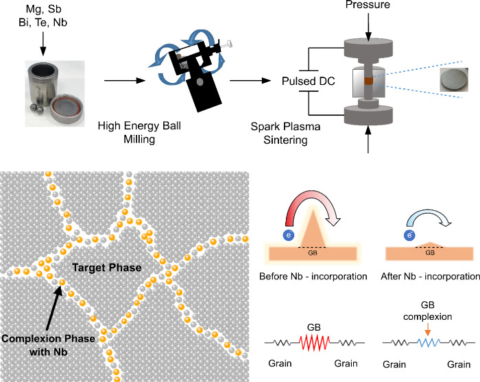
An alternative strategy to tuning the grain size of n-type Mg3Sb2-based materials is modifying the chemical composition of grain boundaries. This has been observed in other thermoelectric materials, particularly in half-Heusler alloys. In Ti-doped NbFeSb, increasing Ti content was found to lower grain boundary resistance through the formation of a Ti-rich phase at the boundaries.52 Similarly, in NbCoSn, Pt dopant segregation reduced scattering from grain boundaries.53 In all such cases, either dopant segregation or secondary phase formation along the boundaries serves to change the energy of the electronic states at the boundary. The effect of the distribution of low-energy grain boundaries on physical properties can be significant, as seen in this study. The structure and chemistry of grain boundaries depend on the type and orientation of the neighboring grains but also on the thermodynamic conditions such as temperature and chemical potential. Thus, grain boundary phases are often called “complexions” to distinguish them from bulk 3D phases (Figure 1). Complexions are essentially 2D phases that exist between 3D grains. Complexions have an energy, defined by the Gibbs excess surface energy and an excess composition (composition differs from neighboring grains) so that the complexion can be engineered with temperature and composition even without grain growth or grain reorientation. In some thermoelectric materials such as n-type Mg3Sb2 the complexions are known to be semiconducting with high interfacial resistance due to Mg deficiency.54 Reducing the impact by growing grains (or single crystals with only low-angle grain boundaries) has been successful in greatly improving thermoelectric performance at low temperatures.3,29−31 In principle, the properties of complexion phases should also depend on chemistry, but this has not been conclusively demonstrated in Mg3(Sb,Bi)2 until now.
Figure 1.

Visualization of the improved electronic properties through grain boundary engineering.
As discussed above, the doping studies previously applied in this system attribute the improvement in zT to factors such as (i) ionized impurity scattering predominating at low temperatures, (ii) substituting Mg to tune carrier concentration, and/or (iii) reducing lattice thermal conductivity due to large atomic mass fluctuations (alloy scattering). However, recent reports using NMR, X-ray absorption spectroscopy (XAS), SEM/TEM, APT have clearly shown no evidence of metal incorporation that would alter the scattering mechanisms in this system.55 Moreover, single crystal studies indicate that ionized impurity scattering does not occur in Mg3Sb2. Instead, the observed increase in electrical conductivity with temperature, seen only in polycrystalline samples, is due to an additional grain boundary electrical resistance, not ionized impurity scattering.55 While several works have explored Nb incorporation into this system, none have explicitly addressed the concept of “grain boundary complexion,″ which is the central focus of our current research. In this work, we provide a detailed examination of how Nb addition modifies the grain boundary without being incorporated into the crystal structure. Specifically, we demonstrate that in Bi-rich Mg3Sb2, the primary effect of Nb is to significantly reduce the grain boundary resistance, even when the grain size remains largely unchanged (Figure 1). This reduction in grain boundary resistance leads to a substantial improvement in zT, achieving a value of 1.14 at 330 K for Mg3.1Nb0.1(Sb0.3Bi0.7)1.996Te0.004, with a high weighted mobility of 335 cm2 V–1 K–1 and a low lattice thermal conductivity of 0.58 W m–1 K–1. For this sample, the device ZT is calculated to be 1.03 at 350 K, which increases to 1.24 at 523 K, and achieves a ηmax of 10.5% at 623 K, highlighting its competitive performance.
2. Experimental Section
2.1. Sample Preparation
Samples of Mg3.2–xNbx(Sb0.3Bi0.7)1.996Te0.004 (x = 0, 0.01, 0,025, 0.05, 0.1, and 0.15) were synthesized by mechanical alloying using a high energy ball mill (SPEX 8000D Mixer/Mill, 1425 rpm). All sample handlings during the synthesis and sintering processes were carried out in an Ar-filled glovebox to avoid oxidation. All the high-purity raw materials of magnesium powder (Mg, 99.8%; Alfa Aesar), bismuth pieces (Bi, 99.999%; Alfa Aesar), antimony shots (Sb, 99.999%; Alfa Aesar), tellurium pieces (Te, 99.9999%; Alfa Aesar), and niobium powder (99.98%, Alfa Aesar) were used without further purification. The stoichiometric amounts of the elements were loaded into a stainless-steel vial with two half-inch stainless steel balls (Figure 1). The mechanical alloying was applied for a duration of 2 h. Following that the resultant powders were loaded into a graphite die and compressed via cold press. For consolidation, spark plasma sintering (SPS) was applied under a uniaxial pressure of 50 MPa for 2 min at 1073 K under vacuum.
2.2. Sample Characterization
The crystal structure and phase purity analyses were carried out with room temperature X-ray diffraction (XRD, Rigaku Mini Flex 600, Cu Kα (λ= 1.5406 Å), 40 kV voltage and 15 mA current). The lattice parameters were refined, and texture analysis was performed using the WinCSD program package.56 The morphology and elemental compositions of the samples were determined by Scanning Electron Microscopy (SEM) and Energy Dispersive X-ray Spectroscopy (EDS), respectively, using a Zeiss Ultra Plus Field Emission Scanning Electron Microscope. Accurate chemical composition analyses were conducted with Wavelength Dispersive X-ray Spectroscopy (WDS) on an electron microprobe (Cameca SX 100, tungsten cathode) considering the line compound Mg2Si and certificated elements of Sb, Bi and Te as references. The high-resolution transmission electron microscopy (HR-TEM) and selected area electron diffraction (SAED) were employed on samples using the Talos F200S scanning/transmission electron microscope (S/TEM) operating with a maximum acceleration voltage of 200 kV.
2.3. Transport Property Measurements
The transport properties of samples were analyzed between 330 and 623 K. The thermal diffusivity, D, of the samples, was measured by Netzsch LFA 467 equipment on disc-shaped geometries (10 mm in diameter). The thermal conductivity, κ, values were then calculated by the relation, κ = D × cp × d, where cp is the specific heat estimated by polynomial equation described by Agne et al.57 (Figure S1), and d is the geometrical density. The S and σ measurements were conducted by Ulvac ZEM-3 device on bar-shaped samples. To achieve the desired geometry, samples were cut with a diamond wire saw. All the transport property measurements were performed along the cross-plane direction, which is parallel to the SPS pressing direction. The average zT values (zTave) of the samples were determined using the formula zTave = ∫ThTczT dT/(Th – Tc), where Th and Tc represent the hot-side and cold-side temperatures, respectively. The thermoelectric device figure of merit, ZT, and the maximum conversion efficiency, ηmax, were calculated according to the method described by Snyder et al.11
2.4. Effective Mass (EM) Model
Carrier concentration (nH)-dependent PF (=S2σ) and zT near room temperature were calculated for x = 0 and 0.05 in Mg3.2–xNbx(Sb0.3Bi0.7)1.996Te0.004 using the Effective Mass (EM) model, assuming acoustic phonon scattering as the dominant carrier scattering mechanism.58 The density-of-states effective mass (md*) was first determined by fitting theoretical S (eq 1) and nH (eq 2) to experimental data. The kB, e, η, h, and Fj are the Boltzmann constant, electric charge, reduced Fermi energy, Planck’s constant, and the Fermi integral of order j (eq 3), respectively:
| 1 |
| 2 |
| 3 |
From the md* and nondegenerate mobility (μ0, Table S3), the weighted mobility (μW) was calculated using eq 4, where me is the electron rest mass. Using the μW, the nH-dependent PF was predicted.
| 4 |
The thermoelectric quality factor (B-factor) was calculated using μW and the lattice thermal conductivity (κl).
| 5 |
The B-factor was used to predict the nH-dependent zT.
2.5. Thermal Conductivity model
The apparent κl (eq 5) near room temperature was obtained by subtracting electronic contribution to κ (κe) from the experimental κ (κl = κ – κe). The κe was, in turn, calculated from Lorenz number (L) and σ (eq 6).
| 6 |
3. Results and Discussion
3.1. Phase and Crystal Structure Analysis
The XRD patterns for pristine and Nb-added samples of Mg3.2–xNbx(Sb0.3Bi0.7)1.996Te0.004 (x = 0, 0.025, 0.05, 0.1 and 0.15) are given in Figure 2a. The XRD pattern of the pristine sample conforms to the trigonal Mg3Bi2 crystal structure (space group: P3̅m1, Figure 2b). However, the Sb3– substitution on Bi3– sites shifts peak positions toward higher 2θ values because of the smaller ionic radius of Sb3– (1.88 Å) compared to Bi3– (1.93 Å). On the other hand, no detectable shift in peak positions is observed for the Nb-added samples due to similar ionic radii of Mg2+ and Nb cations (See Table S1 and Figure S2). A shoulder peak and a low-intensity secondary peak emerged at around 38° and 42° for the samples with x = 0.1 and 0.15, indicating the presence of the cubic Nb3Sb phase (space group: Pm3̅n). This shows that the solubility of Nb in the target phase is significantly lower than the added amounts. This is consistent with the results from Luo et al.33 for Mg3Sb2 that showed only metallic Nb with no detectable incorporation into the target phase.
Figure 2.

a) XRD patterns (Cu–K∝ radiation) of Mg3.2–xNbx(Sb0.3Bi0.7)1.996Te0.004 (x = 0, 0.025, 0.05, 0.1 and 0.15), b) the crystal structure of Mg3(Sb,Bi)2 with possible atom positions.
3.2. Microstructure and HR-TEM Analysis
The EDS mapping of the Mg3.1Nb0.1(Sb0.3Bi0.7)1.996Te0.004 sample is shown in Figure 3. SEM images reveal a homogeneous elemental distribution of Sb, Bi, and Te, with black spots corresponding to the lighter elements of Mg and Nb. The elemental secondary phases are predominantly observed around grain boundaries but within the grains as well. The detection of Te was not possible because of its low concentration. Elemental mapping shows that a significant portion of Nb remains in its elemental form rather than incorporating into the crystal structure. Furthermore, distinct phase differences are discernible in the microstructure, highlighted by variations in contrast. EDS analysis elucidates the elemental distribution: the darker gray areas correspond to 59.9, 25.8, 12.0, and 2.4 at. % of Mg, Bi, Sb, and Nb, respectively. In contrast, brighter areas exhibit concentrations of 59.0, 28.4, 10.6, and 2 at. % of Mg, Bi, Sb, and Nb. Thus, a meaningful difference is observed in the amounts of Bi for the bright and gray areas.
Figure 3.

EDS elemental mapping of the Mg3.1Nb0.1(Sb0.3Bi0.7)1.996Te0.004 sample.
As discussed before, with the increase in Nb addition, the formation of the Nb3Sb secondary phase was observed from the XRD analysis. For further investigation of secondary phases and microstructure, a STEM image was captured from Mg3.05Nb0.15(Sb0.3Bi0.7)1.996Te0.004 sample, to highlight changes more prominently. In Figure 4, the STEM image, along with EDS layered images, elucidates the generation of the Nb3Sb phase within the microstructure. While the secondary phase of elemental Nb remained as small-grain precipitates (approximately 100 nm in size), the Nb3Sb phase manifested as distinct lines within the microstructure.
Figure 4.

a) STEM image of Mg3.05Nb0.15(Sb0.3Bi0.7)1.996Te0.004, b) EDS overall elemental mapping, c) elemental mapping of Sb Lα1 and d) Nb Kα1.
In addition to EDS analysis, WDS analysis was applied to both Nb-added and pristine samples. WDS images and elemental distribution graphs in Figure S3 further corroborate that darker spots correspond to the presence of Mg or Nb. From 10 different spots selected on the BSE image, the average chemical composition was calculated as Mg3.13Nb0.09Sb0.6Bi1.37Te0.003. Given that the spot size of the WDS measurement is approximately 5 μm and secondary phases of Nb are thoroughly precipitated in the microstructure, the incorporation of Nb into the crystal structure of the target phase remains ambiguous.
Since clear estimations of grain boundaries and grains are challenging through SEM analysis, polarized light optical microscopy images were obtained both for the pristine and Nb-added samples. For quantitative average grain size analysis, an image analysis software (MIPAR) was utilized, generating the images provided in Figures 5a-e. The equivalent diameters of the grains were evaluated. The results unveiled essentially the same grain sizes, ranging from 13.97 to 16.52 μm, for pristine and Mg3–xNbx(Sb0.3Bi0.7)1.996Te0.004 (x = 0, 0.025, 0.05, 0.1 and 0.15) samples (Table S2).
Figure 5.

a–e) Grain size analysis of the pristine and Nb added Mg3.2–xNbx(Sb0.3Bi0.7)1.996Te0.004 (x = 0, 0.025, 0.05, 0.1 and 0.15) samples.
Figure 6 presents the backscattered electron-scanning electron microscopy (BSE-SEM) images of both pristine and Nb-added sample of Mg3.1Nb0.1(Sb0.3Bi0.7)1.996Te0.004. In Figure 6a, the darker points observed correspond to the elemental Mg. The regions with different contrasts in BSE-SEM images reveal at least three distinct phases in both samples: a slightly Bi-excess phase, a slightly Bi-deficient phase, and secondary impurity phase manifesting as small black spots. EDS analysis indicates that the brighter areas creating inner grain boundaries possess a higher Bi content compared to the main grains with a gray color (Figure 3). This observation aligns with the study conducted by Sepheri-Amin et al., discussing the brighter contrast of grain boundaries due to a higher concentration of heavier elements in Mg3Sb2–Mg3Bi2 alloys.26 According to the EDS analysis, the overall composition of the pristine sample is Mg3.13Sb0.64Bi1.43 and the Nb-added sample is Mg3.09Nb0.098Sb0.62Bi1.39, which is comparable to the WDS analysis (Figure 3 and S3).
Figure 6.

BSE-SEM images of Mg3.2–xNbx(Sb0.3Bi0.7)1.996Te0.004 for a) x = 0 and b) x = 0.1. c) HR-TEM and d) SAED images for x = 0.1 sample.
The HR-TEM image of a sample with x = 0.1 revealed lattice fringes with spacings of approximately 0.34 and 0.37 nm, corresponding to the (011) planes of Bi-deficient and (002) planes of Bi-excess phases within Mg3(Sb, Bi)2 (Figure 6c). This result indicates that in addition to micron-sized grains, there are nanometer-sized subgrains of the target phase present in the microstructure, suggesting the formation of a mesoscale architecture. Moreover, the SAED analysis of this sample displayed a diffraction pattern with well-defined spots along the [-111] zone axis, consistent with the trigonal crystal structure of Mg3(Sb, Bi)2 (Figure 6d).
3.3. Electronic Transport
From Figure 7a, it is evident that except for the pristine sample, the electrical resistivity (ρ = 1/σ) values of all Nb incorporated samples show a rising trend as the temperature increases in parallel with metal-like behavior. The sample without Nb exhibits a wide U-shaped temperature dependence of ρ due to competition between various carrier scattering mechanisms. At low temperatures, a thermally activated scattering dominates. While this is often attributed to ionized impurity scattering,36 it has been shown conclusively in Mg3Sb2 to be due to charged grain boundaries.46 Also, as shown in Figure S6, due to the scattering attributed to charged grain boundary, the sample without Nb exhibits U-shaped temperature dependence of Hall mobility (μH), a phenomenon reported in various literature.41,59−61 The samples with and without Nb exhibit very similar temperature-dependent Seebeck coefficients (S), as shown in Figure 7c. This similarity suggests comparable doping levels and electron scattering mechanisms within the grains, along with a temperature-dependent weighted mobility (μW). The calculation of μW, band parameter directly proportional to theoretically achievable maximum PF, is utilized to understand influence of complex band behavior on transport properties. At low temperatures, μW increases and then transitions to the typical decreasing trend at higher temperatures, which is more pronounced in the x = 0 and 0.025 samples, as expected due to phonon scattering (Figure 7d).40 Since the μW incorporates the density of states, it is a more robust measure for materials with complex scattering mechanisms like grain boundaries or ionized impurities, which might not be fully captured by Hall effect measurement.62
Figure 7.

a) Electrical resistivity, b) nH (pristine and Nb added (x = 0.05) samples), c) S, d) μW, e) PF, and f) estimated PF (lines) and measured PF (symbols) of pristine and Nb added Mg3.2–xNbx(Sb0.3Bi0.7)1.996Te0.004 (x = 0, 0.025, 0.05, 0.1 and 0.1 5) samples.
The detection of secondary phases, such as Nb3Sb, through XRD (Figure 2a) and STEM images (Figure 4), does not seem to adversely impact ρ values either. In fact, Nb3Sb, known to exhibit superconductivity at very low temperatures, has a high σ with a room temperature resistivity of only 18 μΩ cm, suggesting a positive influence on the overall σ behavior.63,64 Similarly, the presence of Nb as another secondary phase, characterized by high σ, further supports the notion that these secondary phases might not have a detrimental effect on resistivity values. Moreover, the decrease in Sb content within the crystal structure due to secondary phase formation could play a role. Given the electron acceptor role of Sb atoms, a reduction in their quantity could lead to an increase in electron carrier concentration.
The carrier concentration (nH) measurements were conducted on both pristine and Nb-added (x = 0.05) samples. As shown in Figure 7b, the nH exhibited only a slight increase following Nb addition. This observation is consistent with the slight reduction in S (Figure 7c). The decrease in ρ with Nb doping cannot be solely attributed to the increased nH. The μH of the x = 0.05 sample (440 cm2 V–1 s–1) is significantly higher than that of the pristine sample (200 cm2 V–1 s–1) (Figure S4), suggesting an additional factor influencing σ.
The change in σ is primarily attributed to the nature of the grain boundary complexions and a concurrent reduction in the influence of grain boundary scattering. It is well-established that grain boundaries have an important impact on electrical properties, particularly in Mg3Sb2-based thermoelectric materials. This has been shown by observing how the properties change with grain size from BSE-SEM images. Numerous studies have substantiated the impact of grain boundary resistance phenomena, particularly their contribution to elevated ρ values, especially at room temperature.17,22,24,38−42 The presence of Mg deficiencies around grain boundaries adds another layer to the explanation for the observed higher resistivity values.42
However, in this case, the reduction in grain boundary resistance is attributed not to grain growth but to a reduction in the resistance of the average grain boundary. This can be deduced from the polarized light images in Figure 5, illustrating no significant change in grain size upon Nb incorporation. Since there is no strong observable change in grain size to correlate with the reduction in grain boundary scattering upon Nb addition, Nb must be making the boundaries less resistive.
The magnitude of grain boundary scattering is determined by the space charge region that forms. This is possibly a result of a mismatch in conduction or valence band energies between the grain and grain boundary.59,65 For example, in a case where dopant segregation occurs or grain boundary wetting phases are formed, the band energies of the grain boundary region will change, and thus change the mismatch between the bulk and boundary conduction or valence bands. This will either reduce the barrier to conduction if the mismatch is lower or increase it if the mismatch is higher. Since Nb has been observed to form a grain boundary wetting phase in Mg3Sb2,49 this is a possible explanation for the reduction in grain boundary scattering observed between samples with and without Nb.
This band energy mismatch between the boundaries and bulk, or band offset ΔE, can be modeled using a two-phase approach like that used by Kuo et al.40 In this case, a series circuit picture of grain boundary scattering can be used to separate grain and grain boundary contributions to conductivity:
| 7 |
where σg and σgb are the contributions to σ from grain and grain boundaries, respectively, and fgb is the volume fraction of grain boundaries, which can be calculated from the grain size as described by Chookajorn et al.66 This equation can be coupled with the band transport equation for conductivity:
| 8 |
where σE0is the transport coefficient, and s is a conduction mechanism-dependent parameter for the bulk (grain) and (Ef – ΔE)/kBT for the grain boundary phase. Phonon scattering parameters (s = 1 and σE0 ∝ T0) were used for both the grain and grain boundary phase. Single crystal σ values (σg in eq 7) for Mg3.2(Sb0.3Bi0.7)1.996Te0.004 can be calculated at different Fermi levels using eq 8, employing data from two samples with different grain sizes. This single crystal σ can be used to calculate a single crystal μW, which is applicable to all samples with the same Bi–Sb ratio regardless of doping level until the onset of bipolar conduction.62 Using the calculated single crystal conductivity values (σg), eq 7 is applied to determine the grain boundary conductivity (σgb). The parameter s in eq 8 is treated as a constant, chosen by minimizing the root-mean-square error of eq 7 for Mg3.2(Sb0.3Bi0.7)1.996Te0.004 without added Nb. A series of temperature-dependent μW values can be calculated using the two-phase method with those derived from measured S and σ.62 The η value used to calculate the σgb can also be used to find the ΔE between the bulk and the grain boundaries. Figure 8 presents the results of this calculation, demonstrating that samples containing Nb exhibit a significantly lower ΔE compared to pristine samples. To show that this relationship is independent of grain size, we included data from Li et al.51 for a Mg3.2Bi1.49Sb0.5Te0.01 sample with a much smaller grain size of 2.9 μm and Ef of 37 meV. This sample exhibits a similar ΔE to the two samples synthesized in this study, both of which have larger grain sizes (>10 μm).
Figure 8.

Modeled ΔE versus bulk Ef for Mg3.2–xNbx(Sb0.3Bi0.7)1.996Te0.004 and one Mg3.2Bi1.49Sb0.5Te0.01 sample from Liu et al.9
The model results indicate that the addition of Nb reduces ΔE, thereby decreasing the scattering strength of grain boundaries in Mg3Sb2. This effect is consistent across different grain sizes and doping levels, suggesting that the formation of the Nb wetting phase and resulting reduction in ΔE are the primary factors driving the decrease in grain boundary scattering with Nb addition.
Figure 7c demonstrates consistent n-type behavior across all samples, irrespective of Nb content. The decrease in S observed above 473 K is interpreted as compelling evidence of a bipolar effect.
The μW values of the samples were estimated from the experimental S and ρ data (Figure 7d).62 The μW, which is independent of the chemical potential and nH, or the doping element, is an important band parameter for determining the electronic properties of thermoelectric materials.4,26,62 The onset of bipolar conduction observed in the S data above 473 K, attributed to a narrower band gap, leads to a decrease in the μW values.26 Consequently, comparisons of μW values below 473 K more accurately reflect the electronic band structures of the samples. Notably, after Nb metal addition, all μW values consistently increased, reaching a range of 280–330 cm2 V–1 s–1 at 330 K, regardless of the quantity of added Nb. In the temperature range of 330–450 K, the μW values exhibited a consistent increase with Nb addition (x = 0.025, 0.05, and 0.1), surpassing those of other promising low-temperature Mg3Sb2–Mg3Bi2 alloys where μW typically range between 180 and 250 cm2 V–1 s–1.17 This improvement stems from grain boundary complexions and the overall larger grain size compared to other studies. For example, at 330 K, the μW of the Nb-added sample with x = 0.1 (330 cm2 V–1 s–1) shows approximately 130% improvement over the pristine sample (142 cm2 V–1 s–1). Since the thermoelectric quality factor (B-factor in eq 5) is directly related to μW values,67,68 this substantial improvement also correlates with an enhancement in the theoretical maximum zT. The μW itself is also linked to the theoretical maximum PF. Experimentally, the PF of the Nb-added sample with x = 0.1 (33.5 μW cm–1 K–2) shows approximately 148% improvement compared to the pristine sample (13.5 μW cm–1 K–2) (Figure 7e). An even larger improvement, as predicted by the μW change, is possible if the nH of the pristine sample is different from the optimum for the highest PF. Using the EM model, nH-dependent PF for the pristine and Nb-added sample with x = 0.05 are calculated (Figure 7f). As expected, the experimental nH of the pristine sample (8 × 1018 cm–3) is lower than the optimum nH for maximizing the PF, which is 2 × 1019 cm–3. We also observe that the nH of the Nb-added sample with x = 0.05 is relatively closer to this optimal nH (Figure S4 and Table S3).
3.4. Thermal Transport
Figure 9a presents experimental κ as a function of temperature. Both pristine and Nb-added samples exhibit a rising trend in κ with increasing temperature. Especially the pronounced increase in κ observed above 450 K coincides with the onset of the bipolar conduction demonstrated by the temperature-dependent S in Figure 7c. The EM model was used to estimate the electronic contribution (κe) to κ for pristine and Nb-added samples (Figure 9b). The apparent lower κe of the pristine sample compared to the Nb-added samples near room temperature is attributed to the low σgb of the pristine sample, as demonstrated by Kuo et al.69 Given that the S is essentially the same for all samples (Figure 7c), it can be inferred that the σg is similar, and consequently, the κe is also comparable across samples. Figure 9b also presents the κe estimated by using σg instead of experimental σ in eq 6 (empty symbols). The close agreement between these values supports our inference about the similarity of σg across samples. The κe (Figure 9b) was subtracted from the κ (Figure 9a), to obtain the sum of lattice thermal conductivity (κl) and bipolar thermal conductivity (κbi), as shown in Figure 9c. The sum of κl and κbi estimated using κe derived from σg is also presented (empty symbols). After accounting for grain boundary scattering, the apparent higher κl of the pristine sample (filled symbols) becomes comparable to other Nb-added samples (empty symbols). Hence, Nb and Nb3Sb phases (observed in x ≥ 0.1 samples) were ineffective in suppressing κl.
Figure 9.

a) κ, b) κe, and c) sum of κl and κbi of pristine and Nb-added Mg3.2–xNbx(Sb0.3Bi0.7)1.996Te0.004 (x = 0, 0.025, 0.05, 0.1 and 0.1 5) samples.
3.5. Thermoelectric Figure of Merit
Figure 10 presents the temperature-dependent zT and B-factor, along with the theoretically achievable zT as a function of nH. The combined effect of low κl and high μW, achieved through reduced grain boundary scattering, results in a zT exceeding 1 for Nb-doped samples between 330 and 423 K, making them competitive with state-of-the-art Bi2Te3 alloys.
Figure 10.

Temperature-dependent a) zT (Liu et al.17) in dashed line) and b) B-factor of pristine and Nb-added Mg3.2–xNbx(Sb0.3Bi0.7)1.996Te0.004 (x = 0, 0.025, 0.05, 0.1 and 0.15) samples. (c) Calculated and measured nH-dependent zT of pristine and x = 0.05 samples, and d) calculated device ZT and ηmax of x = 0.1 sample.
As shown in Figure 10a, the sample with x = 0.025 exhibits a peak zT of 1.43 at 450 K, the highest among all investigated compositions. Notably, the zT of the x = 0.1 sample reaches 1.14 near room temperature, surpassing all reported Mg3(Sb,Bi)2-based materials. For comparison, the high zT of Cu-doped Mg3(Sb,Bi)2 by Liu et al. (dashed line) is included. To ensure reproducibility, an additional sample with identical composition was prepared, demonstrating comparable zT (Figure S5). The x = 0.025 sample achieves an average zT of 1.22 between 330 and 573 K. Figure 10b confirms the correlation between Nb doping and increased B-factors (proportional to μW/κl in eq 5), which reflect the theoretical maximum zT.
Figure 10c presents the calculated nH-dependent zT for pristine and Nb-doped (x = 0.05) samples. The lines represent the theoretically achievable zT calculated using the EM model. Notably, the zT of the x = 0.05 sample could potentially reach ∼1.05 at an nH of 7 × 1018 cm–3. However, the measured zT already approaches 1.01 at 330 K, suggesting near-optimal nH in x = 0.05 sample.
The calculated device ZT for Mg3.1Nb0.1(Sb0.3Bi0.7)1.996Te0.004 ranges from 1.03 to 1.24 within the temperature range of 350 to 623 K, as presented in Figure 8d.70 At 623 K, the theoretical maximum device efficiency (ηmax) reaches an impressive 10.5%, demonstrating highly competitive performance.
4. Conclusions
The Mg3(Sb,Bi)2 system has been significantly modified through the incorporation of Nb, reducing the grain boundary electrical resistance. While in Mg3Sb2 the primary effect of Nb is to facilitate grain growth, the samples prepared here show little change in grain size. Instead, the resistivity of the grain boundaries themselves is dramatically reduced. The reduction is so significant that the conductivity and mobility have little indication of grain boundary resistance. This study shows that the properties of the grain boundary complexion phase itself in Mg3(Sb,Bi)2 can be modified with chemical processing. The achievement of low thermal conductivity in the range of 0.9–1 W m–1 K–1, coupled with low resistivity values and elevated carrier mobility, has contributed to the attainment of high zT values, particularly in low-temperature regimes. Notably, our study has yielded a record-high zT of 1.14 at 330 K, with a device ZT of 1.03 at 350 K, reaching 1.24 at 523 K, and achieving a ηmax of 10.5% at 623 K, highlighting its competitive performance. Our work encourages the exploration of Mg3(Sb,Bi)2 as an alternative thermoelectric material for room-temperature applications, challenging the dominance of traditional materials like Bi2Te3. The emphasis on microstructure engineering, specifically the chemistry of grain boundary complexion phases, emerges as a promising avenue for further enhancing the thermoelectric properties of these materials.
Acknowledgments
This work is supported financially by Turkish Aerospace with project number TM4111 and the Scientific and Technological Research Council of Türkiye (TUBITAK) with project numbers 20AG001 and 20AG020. U.A. acknowledges Barış Yağcı and other researchers at Koç University Surface Science and Technology Center (KUYTAM) for SEM measurements. U.A. would also like to thank Dr. Süleyman Tekmen from Bayburt University Central Research Laboratory (BUMER) and Gülcan Çorapcıoğlu from the Central Research Facility (n2STAR) of Koç University for the HRTEM and SAED measurements
Supporting Information Available
The Supporting Information is available free of charge at https://pubs.acs.org/doi/10.1021/acsami.4c12046.
Comprehensive data and analyses related to heat capacity, XRD patterns and lattice parameters, SEM images and grain size analysis, effective mass analysis, thermoelectric transport properties, and Hall and weighted mobility (PDF)
The authors declare no competing financial interest.
Supplementary Material
References
- Fragkos P.; Tasios N.; Paroussos L.; Capros P.; Tsani S. Energy system impacts and policy implications of the European Intended Nationally Determined Contribution and low-carbon pathway to 2050. Energy Policy 2017, 100, 216–226. 10.1016/j.enpol.2016.10.023. [DOI] [Google Scholar]
- Liang Z.; Xu C.; Song S.; Shi X.; Ren W.; Ren Z. Enhanced Thermoelectric Performance of p-Type Mg3Sb2 for Reliable and Low-Cost all-Mg3Sb2-Based Thermoelectric Low-Grade Heat Recovery. Adv. Funct. Mater. 2023, 33 (7), 2210016. 10.1002/adfm.202210016. [DOI] [Google Scholar]
- Liu Z.; Sato N.; Gao W.; Yubuta K.; Kawamoto N.; Mitome M.; Kurashima K.; Owada Y.; Nagase K.; Lee C. H.; Yi J.; Tsuchiya K.; Mori T. Demonstration of ultrahigh thermoelectric efficiency of∼ 7.3% in Mg3Sb2/MgAgSb module for low-temperature energy harvesting. Joule 2021, 5 (5), 1196–1208. 10.1016/j.joule.2021.03.017. [DOI] [Google Scholar]
- Imasato K.; Kang S. D.; Snyder G. J. Exceptional thermoelectric performance in Mg 3 Sb 0.6 Bi 1.4 for low-grade waste heat recovery. Energy Environ. Sci. 2019, 12 (3), 965–971. 10.1039/C8EE03374A. [DOI] [Google Scholar]
- Mao J.; Chen G.; Ren Z. Thermoelectric cooling materials. Nat. Mater. 2021, 20 (4), 454–461. 10.1038/s41563-020-00852-w. [DOI] [PubMed] [Google Scholar]
- Liu W.; Yan X.; Chen G.; Ren Z. Recent advances in thermoelectric nanocomposites. Nano Energy 2012, 1 (1), 42–56. 10.1016/j.nanoen.2011.10.001. [DOI] [Google Scholar]
- Jood P.; Male J. P.; Anand S.; Matsushita Y.; Takagiwa Y.; Kanatzidis M. G.; Snyder G. J.; Ohta M. Na Doping in PbTe: Solubility, Band Convergence, Phase Boundary Mapping, and Thermoelectric Properties. J. Am. Chem. Soc. 2020, 142 (36), 15464–15475. 10.1021/jacs.0c07067. [DOI] [PubMed] [Google Scholar]
- Heremans J. P.; Jovovic V.; Toberer E. S.; Saramat A.; Kurosaki K.; Charoenphakdee A.; Yamanaka S.; Snyder G. J. Enhancement of Thermoelectric Efficiency in PbTe by Distortion of the Electronic Density of States. Science 2008, 321 (5888), 554–557. 10.1126/science.1159725. [DOI] [PubMed] [Google Scholar]
- Liu H.-T.; Sun Q.; Zhong Y.; Deng Q.; Gan L.; Lv F.-L.; Shi X.-L.; Chen Z.-G.; Ang R. High-performance in n-type PbTe-based thermoelectric materials achieved by synergistically dynamic doping and energy filtering. Nano Energy 2022, 91, 106706 10.1016/j.nanoen.2021.106706. [DOI] [Google Scholar]
- Li H.; Su X.; Tang X.; Zhang Q.; Uher C.; Snyder G. J.; Aydemir U. Grain boundary engineering with nano-scale InSb producing high performance InxCeyCo4Sb12+z skutterudite thermoelectrics. Journal of Materiomics 2017, 3 (4), 273–279. 10.1016/j.jmat.2017.07.003. [DOI] [Google Scholar]
- Zong P.-a.; Hanus R.; Dylla M.; Tang Y.; Liao J.; Zhang Q.; Snyder G. J.; Chen L. Skutterudite with graphene-modified grain-boundary complexion enhances zT enabling high-efficiency thermoelectric device. Energy Environ. Sci. 2017, 10 (1), 183–191. 10.1039/C6EE02467J. [DOI] [Google Scholar]
- Uher C., Chapter One - Roadmap for skutterudites: Prospective novel thermoelectrics. In Semiconductors and Semimetals, Mi Z.; Tan H. H., Eds. Elsevier:2022; Vol. 111, pp 1–5. [Google Scholar]
- Rogl G.; Bursik J.; Grytsiv A.; Puchegger S.; Soprunyuk V.; Schranz W.; Yan X.; Bauer E.; Rogl P. Nanostructuring as a tool to adjust thermal expansion in high ZT skutterudites. Acta Mater. 2018, 145, 359–368. 10.1016/j.actamat.2017.12.001. [DOI] [Google Scholar]
- Rogl G.; Rogl P. F. Development of Thermoelectric Half-Heusler Alloys over the Past 25 Years. Crystals 2023, 13 (7), 1152. 10.3390/cryst13071152. [DOI] [Google Scholar]
- Berry T.; Fu C.; Auffermann G.; Fecher G. H.; Schnelle W.; Serrano-Sanchez F.; Yue Y.; Liang H.; Felser C. Enhancing Thermoelectric Performance of TiNiSn Half-Heusler Compounds via Modulation Doping. Chem. Mater. 2017, 29 (16), 7042–7048. 10.1021/acs.chemmater.7b02685. [DOI] [Google Scholar]
- Zhu H.; Mao J.; Li Y.; Sun J.; Wang Y.; Zhu Q.; Li G.; Song Q.; Zhou J.; Fu Y.; He R.; Tong T.; Liu Z.; Ren W.; You L.; Wang Z.; Luo J.; Sotnikov A.; Bao J.; Nielsch K.; Chen G.; Singh D. J.; Ren Z. Discovery of TaFeSb-based half-Heuslers with high thermoelectric performance. Nat. Commun. 2019, 10 (1), 270. 10.1038/s41467-018-08223-5. [DOI] [PMC free article] [PubMed] [Google Scholar]
- Liu Z.; Gao W.; Oshima H.; Nagase K.; Lee C. H.; Mori T. Maximizing the performance of n-type Mg3Bi2 based materials for room-temperature power generation and thermoelectric cooling. Nat. Commun. 2022, 13 (1), 1120. 10.1038/s41467-022-28798-4. [DOI] [PMC free article] [PubMed] [Google Scholar]
- Ying P.; Wilkens L.; Reith H.; Rodriguez N. P.; Hong X.; Lu Q.; Hess C.; Nielsch K.; He R. A robust thermoelectric module based on MgAgSb/Mg 3 (Sb, Bi) 2 with a conversion efficiency of 8.5% and a maximum cooling of 72 K. Energy Environ. Sci. 2022, 15 (6), 2557–2566. 10.1039/D2EE00883A. [DOI] [Google Scholar]
- Zhang F.; Chen C.; Yao H.; Bai F.; Yin L.; Li X.; Li S.; Xue W.; Wang Y.; Cao F.; Liu X.; Sui J.; Zhang Q. High-performance N-type Mg3Sb2 towards thermoelectric application near room temperature. Adv. Funct. Mater. 2020, 30 (5), 1906143. 10.1002/adfm.201906143. [DOI] [Google Scholar]
- Shi X.; Sun C.; Bu Z.; Zhang X.; Wu Y.; Lin S.; Li W.; Faghaninia A.; Jain A.; Pei Y. Revelation of inherently high mobility enables Mg3Sb2 as a sustainable alternative to n-Bi2Te3 thermoelectrics. Adv. Sci. 2019, 6 (16), 1802286. 10.1002/advs.201802286. [DOI] [PMC free article] [PubMed] [Google Scholar]
- Shi X.; Sun C.; Zhang X.; Chen Z.; Lin S.; Li W.; Pei Y. Efficient Sc-doped Mg3. 05–x Sc x SbBi thermoelectrics near room temperature. Chem. Mater. 2019, 31 (21), 8987–8994. 10.1021/acs.chemmater.9b03156. [DOI] [Google Scholar]
- Mao J.; Zhu H.; Ding Z.; Liu Z.; Gamage G. A.; Chen G.; Ren Z. High thermoelectric cooling performance of n-type Mg3Bi2-based materials. Science 2019, 365 (6452), 495–498. 10.1126/science.aax7792. [DOI] [PubMed] [Google Scholar]
- Sun X.; Li X.; Yang J.; Xi J.; Nelson R.; Ertural C.; Dronskowski R.; Liu W.; Snyder G. J.; Singh D. J.; Zhang W. Achieving band convergence by tuning the bonding ionicity in n-type Mg3Sb2. J. Comput. Chem. 2019, 40 (18), 1693–1700. 10.1002/jcc.25822. [DOI] [PubMed] [Google Scholar]
- Bhardwaj A.; Rajput A.; Shukla A.; Pulikkotil J.; Srivastava A.; Dhar A.; Gupta G.; Auluck S.; Misra D.; Budhani R. Mg 3 Sb 2-based Zintl compound: a non-toxic, inexpensive and abundant thermoelectric material for power generation. RSC Adv. 2013, 3 (22), 8504–8516. 10.1039/c3ra40457a. [DOI] [Google Scholar]
- Kanno T.; Tamaki H.; Yoshiya M.; Uchiyama H.; Maki S.; Takata M.; Miyazaki Y. High-density frenkel defects as origin of n-Type thermoelectric performance and low thermal conductivity in Mg3Sb2-based materials. Adv. Funct. Mater. 2021, 31 (13), 2008469. 10.1002/adfm.202008469. [DOI] [Google Scholar]
- Sepehri-Amin H.; Imasato K.; Wood M.; Kuo J. J.; Snyder G. J. Evolution of Nanometer-Scale Microstructure within Grains and in the Intergranular Region in Thermoelectric Mg3 (Sb, Bi) 2 Alloys. ACS Appl. Mater. Interfaces 2022, 14 (33), 37958–37966. 10.1021/acsami.2c09905. [DOI] [PubMed] [Google Scholar]
- Wood M.; Kuo J. J.; Imasato K.; Snyder G. J. Improvement of low-temperature zT in a Mg3Sb2–Mg3Bi2 solid solution via Mg-vapor annealing. Adv. Mater. 2019, 31 (35), 1902337. 10.1002/adma.201902337. [DOI] [PubMed] [Google Scholar]
- Ozen M.; Yahyaoglu M.; Candolfi C.; Veremchuk I.; Kaiser F.; Burkhardt U.; Snyder G. J.; Grin Y.; Aydemir U. Enhanced thermoelectric performance in Mg 3+ x Sb 1.5 Bi 0.49 Te 0.01 via engineering microstructure through melt-centrifugation. Journal of Materials Chemistry A 2021, 9 (3), 1733–1742. 10.1039/D0TA09993G. [DOI] [Google Scholar]
- Imasato K.; Fu C.; Pan Y.; Wood M.; Kuo J. J.; Felser C.; Snyder G. J. Metallic N-type Mg3Sb2 single crystals demonstrate the absence of ionized impurity scattering and enhanced thermoelectric performance. Adv. Mater. 2020, 32 (16), 1908218. 10.1002/adma.201908218. [DOI] [PubMed] [Google Scholar]
- Kanno T.; Tamaki H.; Sato H. K.; Kang S. D.; Ohno S.; Imasato K.; Kuo J. J.; Snyder G. J.; Miyazaki Y. Enhancement of average thermoelectric figure of merit by increasing the grain-size of Mg3. 2Sb1. 5Bi0. 49Te0. 01. Appl. Phys. Lett. 2018, 112 (3), 033903 10.1063/1.5016488. [DOI] [Google Scholar]
- Imasato K.; Wood M.; Kuo J. J.; Snyder G. J. Improved stability and high thermoelectric performance through cation site doping in n-type La-doped Mg 3 Sb 1.5 Bi 0.5. Journal of Materials Chemistry A 2018, 6 (41), 19941–19946. 10.1039/C8TA08975B. [DOI] [Google Scholar]
- Zhang J.; Song L.; Pedersen S. H.; Yin H.; Hung L. T.; Iversen B. B. Discovery of high-performance low-cost n-type Mg3Sb2-based thermoelectric materials with multi-valley conduction bands. Nat. Commun. 2017, 8 (1), 13901. 10.1038/ncomms13901. [DOI] [PMC free article] [PubMed] [Google Scholar]
- Luo T.; Kuo J. J.; Griffith K. J.; Imasato K.; Cojocaru-Mirédin O.; Wuttig M.; Gault B.; Yu Y.; Snyder G. J. Nb-Mediated Grain Growth and Grain-Boundary Engineering in Mg3Sb2-Based Thermoelectric Materials. Adv. Funct. Mater. 2021, 31 (28), 2100258. 10.1002/adfm.202100258. [DOI] [Google Scholar]
- Shi X.; Zhang X.; Ganose A.; Park J.; Sun C.; Chen Z.; Lin S.; Li W.; Jain A.; Pei Y. Compromise between band structure and phonon scattering in efficient n-Mg3Sb2-xBix thermoelectrics. Materials Today Physics 2021, 18, 100362 10.1016/j.mtphys.2021.100362. [DOI] [Google Scholar]
- Yang J.; Li G.; Zhu H.; Chen N.; Lu T.; Gao J.; Guo L.; Xiang J.; Sun P.; Yao Y.; Yang R.; Zhao H. Next-generation thermoelectric cooling modules based on high-performance Mg3 (Bi, Sb) 2 material. Joule 2022, 6 (1), 193–204. 10.1016/j.joule.2021.11.008. [DOI] [Google Scholar]
- Shuai J.; Mao J.; Song S.; Zhu Q.; Sun J.; Wang Y.; He R.; Zhou J.; Chen G.; Singh D. J.; Ren Z. Tuning the carrier scattering mechanism to effectively improve the thermoelectric properties. Energy Environ. Sci. 2017, 10 (3), 799–807. 10.1039/C7EE00098G. [DOI] [Google Scholar]
- Shu R.; Zhou Y.; Wang Q.; Han Z.; Zhu Y.; Liu Y.; Chen Y.; Gu M.; Xu W.; Wang Y.; Zhang W.; Huang L.; Liu W. Mg3+ δSbxBi2– x Family: A Promising Substitute for the State-of-the-Art n-Type Thermoelectric Materials near Room Temperature. Adv. Funct. Mater. 2019, 29 (4), 1807235. 10.1002/adfm.201970020. [DOI] [Google Scholar]
- Shi X.; Zhao T.; Zhang X.; Sun C.; Chen Z.; Lin S.; Li W.; Gu H.; Pei Y. Extraordinary n-type Mg3SbBi thermoelectrics enabled by Yttrium doping. Adv. Mater. 2019, 31 (36), 1903387. 10.1002/adma.201903387. [DOI] [PubMed] [Google Scholar]
- Liang Z.; Xu C.; Shang H.; Zhu Q.; Ding F.; Mao J.; Ren Z. High thermoelectric energy conversion efficiency of a unicouple of n-type Mg3Bi2 and p-type Bi2Te3. Materials Today Physics 2021, 19, 100413 10.1016/j.mtphys.2021.100413. [DOI] [Google Scholar]
- Kuo J. J.; Kang S. D.; Imasato K.; Tamaki H.; Ohno S.; Kanno T.; Snyder G. J. Grain boundary dominated charge transport in Mg 3 Sb 2-based compounds. Energy Environ. Sci. 2018, 11 (2), 429–434. 10.1039/C7EE03326E. [DOI] [Google Scholar]
- Qiu Q.; Liu Y.; Xia K.; Fang T.; Yu J.; Zhao X.; Zhu T. Grain boundary scattering of charge transport in n-type (Hf, Zr) CoSb half-Heusler thermoelectric materials. Adv. Energy Mater. 2019, 9 (11), 1803447. 10.1002/aenm.201803447. [DOI] [Google Scholar]
- Gorai P.; Ortiz B. R.; Toberer E. S.; Stevanović V. Investigation of n-type doping strategies for Mg3Sb2. Journal of Materials Chemistry A 2018, 6 (28), 13806–13815. 10.1039/C8TA03344G. [DOI] [Google Scholar]
- Mao J.; Shuai J.; Song S.; Wu Y.; Dally R.; Zhou J.; Liu Z.; Sun J.; Zhang Q.; dela Cruz C.; Wilson S.; Pei Y.; Singh D. J.; Chen G.; Chu C.-W.; Ren Z. Manipulation of ionized impurity scattering for achieving high thermoelectric performance in n-type Mg3Sb2-based materials. Proc. Natl. Acad. Sci. U. S. A. 2017, 114 (40), 10548–10553. 10.1073/pnas.1711725114. [DOI] [PMC free article] [PubMed] [Google Scholar]
- Mao J.; Wu Y.; Song S.; Zhu Q.; Shuai J.; Liu Z.; Pei Y.; Ren Z. Defect engineering for realizing high thermoelectric performance in n-type Mg3Sb2-based materials. ACS Energy Letters 2017, 2 (10), 2245–2250. 10.1021/acsenergylett.7b00742. [DOI] [Google Scholar]
- He J. The Roles of Grain Boundaries in Thermoelectric Transports. Materials Lab 2022, 1 (1), 220012. 10.54227/mlab.20220012. [DOI] [Google Scholar]
- Kuo J. J.; Kang S. D.; Imasato K.; Tamaki H.; Ohno S.; Kanno T.; Snyder G. J. Grain boundary dominated charge transport in Mg3Sb2-based compounds. Energy Environ. Sci. 2018, 11 (2), 429–434. 10.1039/C7EE03326E. [DOI] [Google Scholar]
- Li J.; Liu W.; Xu W.; Zhuang H.; Han Z.; Jiang F.; Zhang P.; Hu H.; Gao H.; Jiang Y.; Cai B.; Pei J.; Su B.; Li Q.; Hayashi K.; Li H.; Miyazaki Y.; Cao X.; Zheng Q.; Li J. Bi-Deficiency Leading to High-Performance in Mg3 (Sb, Bi) 2-Based Thermoelectric Materials. Adv. Mater. 2023, 2209119. 10.1002/adma.202209119. [DOI] [PubMed] [Google Scholar]
- Gorai P.; Ortiz B. R.; Toberer E. S.; Stevanović V. Investigation of n-type doping strategies for Mg 3 Sb 2. Journal of Materials Chemistry A 2018, 6 (28), 13806–13815. 10.1039/C8TA03344G. [DOI] [Google Scholar]
- Luo T.; Kuo J. J.; Griffith K. J.; Imasato K.; Cojocaru-Mirédin O.; Wuttig M.; Gault B.; Yu Y.; Snyder G. J. Nb-mediated grain growth and grain-boundary engineering in Mg3Sb2-based thermoelectric materials. Adv. Funct. Mater. 2021, 31 (28), 2100258. 10.1002/adfm.202100258. [DOI] [Google Scholar]
- Li J. W.; Han Z.; Yu J.; Zhuang H. L.; Hu H.; Su B.; Li H.; Jiang Y.; Chen L.; Liu W.; Zheng Q.; Li J. F. Wide-temperature-range thermoelectric n-type Mg3(Sb,Bi)2 with high average and peak zT values. Nat. Commun. 2023, 14 (1), 7428. 10.1038/s41467-023-43228-9. [DOI] [PMC free article] [PubMed] [Google Scholar]
- Li X.; Sun C.; Yang K.; Liang D.; Ye X.; Song W.; Xu W.; Zhao W.; Zhang Q. Excellent Room Temperature Thermoelectric Performance in Mg3Sb2-Based Alloys via Multi-Functional Doping of Nb. Small 2024, 20, 2311478. 10.1002/smll.202311478. [DOI] [PubMed] [Google Scholar]
- Bueno Villoro R.; Zavanelli D.; Jung C.; Mattlat D. A.; Hatami Naderloo R.; Pérez N.; Nielsch K.; Snyder G. J.; Scheu C.; He R.; Zhang S. Grain Boundary Phases in NbFeSb Half-Heusler Alloys: A New Avenue to Tune Transport Properties of Thermoelectric Materials. Adv. Energy Mater. 2023, 13 (13), 2204321. 10.1002/aenm.202204321. [DOI] [Google Scholar]
- Luo T.; Serrano-Sánchez F.; Bishara H.; Zhang S.; Bueno Villoro R.; Kuo J. J.; Felser C.; Scheu C.; Snyder G. J.; Best J. P.; Dehm G.; Yu Y.; Raabe D.; Fu C.; Gault B. Dopant-segregation to grain boundaries controls electrical conductivity of n-type NbCo(Pt)Sn half-Heusler alloy mediating thermoelectric performance. Acta Mater. 2021, 217, 117147 10.1016/j.actamat.2021.117147. [DOI] [Google Scholar]
- Kuo J. J.; Yu Y.; Kang S. D.; Cojocaru-Mirédin O.; Wuttig M.; Snyder G. J. Mg Deficiency in Grain Boundaries of n-Type Mg3Sb2 Identified by Atom Probe Tomography. Adv. Maters Interfaces 2019, 6 (13), 1900429. 10.1002/admi.201900429. [DOI] [Google Scholar]
- Imasato K.; Wood M.; Anand S.; Kuo J. J.; Snyder G. J. Understanding the High Thermoelectric Performance of Mg3Sb2-Mg3Bi2 Alloys. Adv. Energy Sustainability Res. 2022, 3 (6), 2100208. 10.1002/aesr.202100208. [DOI] [Google Scholar]
- Akselrud L.; Grin Y. WinCSD: software package for crystallographic calculations (Version 4). J. Appl. Crystallogr. 2014, 47 (2), 803–805. 10.1107/S1600576714001058. [DOI] [Google Scholar]
- Agne M. T.; Imasato K.; Anand S.; Lee K.; Bux S. K.; Zevalkink A.; Rettie A. J.; Chung D. Y.; Kanatzidis M. G.; Snyder G. J. Heat capacity of Mg3Sb2, Mg3Bi2, and their alloys at high temperature. Materials Today Physics 2018, 6, 83–88. 10.1016/j.mtphys.2018.10.001. [DOI] [Google Scholar]
- May A. F.; Snyder G. J.. Introduction to modeling thermoelectric transport at high temperatures. Materials, preparation, and characterization in thermoelectrics; CRC Press; 2012, 1–18.. [Google Scholar]
- Hu C.; Xia K.; Fu C.; Zhao X.; Zhu T. Carrier grain boundary scattering in thermoelectric materials. Energy Environ. Sci. 2022, 15 (4), 1406–1422. 10.1039/D1EE03802H. [DOI] [Google Scholar]
- He R.; Kraemer D.; Mao J.; Zeng L.; Jie Q.; Lan Y.; Li C.; Shuai J.; Kim H. S.; Liu Y.; Broido D.; Chu C. W.; Chen G.; Ren Z. Achieving high power factor and output power density in p-type half-Heuslers Nb1-xTixFeSb. Proc. Natl. Acad. Sci. U. S. A. 2016, 113 (48), 13576–13581. 10.1073/pnas.1617663113. [DOI] [PMC free article] [PubMed] [Google Scholar]
- Wei T.-R.; Wu C.-F.; Zhang X.; Tan Q.; Sun L.; Pan Y.; Li J.-F. Thermoelectric transport properties of pristine and Na-doped SnSe 1– x Te x polycrystals. Phys. Chem. Chem. Phys. 2015, 17 (44), 30102–30109. 10.1039/C5CP05510E. [DOI] [PubMed] [Google Scholar]
- Snyder G. J.; Snyder A. H.; Wood M.; Gurunathan R.; Snyder B. H.; Niu C. Weighted mobility. Adv. Mater. 2020, 32 (25), 2001537. 10.1002/adma.202001537. [DOI] [PubMed] [Google Scholar]
- Williamson S.; Milewits M. In Evidence for Selective Electron-Phonon Scattering in the A-15 Superconductors Nb 3 Sn, Nb 3 Sb, and V 3 Si, Superconductivity in d-and f-Band Metals: Second Rochester Conference; Springer:1976; pp 551–565. [Google Scholar]
- Chen Q.; Zhou Y.; Xu B.; Lou Z.; Chen H.; Chen S.; Wu C.; Du J.; Wang H.; Yang J.; Fang M. Large Magnetoresistance and Nontrivial Berry Phase in Nb3Sb Crystals with A15 Structure. Chin. Phys. Lett. 2021, 38 (8), 087501 10.1088/0256-307X/38/8/087501. [DOI] [Google Scholar]
- Seto J. Y. W. The electrical properties of polycrystalline silicon films. J. Appl. Phys. 1975, 46 (12), 5247–5254. 10.1063/1.321593. [DOI] [Google Scholar]
- Chookajorn T.; Murdoch H. A.; Schuh C. A. Design of Stable Nanocrystalline Alloys. Science 2012, 337 (6097), 951–954. 10.1126/science.1224737. [DOI] [PubMed] [Google Scholar]
- Wang H.; Pei Y.; LaLonde A. D.; Jeffery Snyder G., Material design considerations based on thermoelectric quality factor. Thermoelectric Nanomaterials: Materials Design and Applications; Springer Science & Business; 2013, 3–32.
- Witting I. T.; Chasapis T. C.; Ricci F.; Peters M.; Heinz N. A.; Hautier G.; Snyder G. J. The thermoelectric properties of bismuth telluride. Advanced Electronic Materials 2019, 5 (6), 1800904. 10.1002/aelm.201800904. [DOI] [Google Scholar]
- Kuo J. J.; Wood M.; Slade T. J.; Kanatzidis M. G.; Snyder G. J. Systematic over-estimation of lattice thermal conductivity in materials with electrically-resistive grain boundaries. Energy Environ. Sci. 2020, 13 (4), 1250–1258. 10.1039/C9EE03921J. [DOI] [Google Scholar]
- Snyder G. J.; Snyder A. H. Figure of merit ZT of a thermoelectric device defined from materials properties. Energy Environ. Sci. 2017, 10 (11), 2280–2283. 10.1039/C7EE02007D. [DOI] [Google Scholar]
Associated Data
This section collects any data citations, data availability statements, or supplementary materials included in this article.