Open Research Europe logoLink to Open Research Europe
. 2024 Nov 11;4:97. Originally published 2024 Apr 29. [Version 2] doi: 10.12688/openreseurope.17481.2

Development of flip-chip technology for the optical drive of superconducting circuits

Oliver Kieler 1,a, Hao Tian 1, Marco Kraus 1, Shekhar Priyadarshi 1, Judith Felgner 1, Alexander Fernandez Scarioni 1, Johannes Kohlmann 1, Mark Bieler 1
PMCID: PMC11585851  PMID: 39582834

Version Changes

Revised. Amendments from Version 1

Section 2: We added details about stud-bump size and CPW dimensions. Section 3: Some explanation about the optimization of flip-chip bonding force and its influence on the bump deformation was included. Information about possible cracks in the bond connection after several cooling cycles was added, indicating that we did not observe any issues. This includes information about delamination, bond-pad material and usage of external force. The investigation of the flip-chip bonded devices at high-speed (using femto-second lasers) showed no issues too, which is clear evidence about the high-quality bonding connection. The meaning of yield in percentage was explained in more detail with respect to the number of working devices.   The standard uncertainty was introduced to quantitatively analyze the alignment precision of the sleeve mount. We did not make any SEM images of the sleeves after several cool-down cycles, but we confirmed that no issues were observed. Section 4: We added a short comment that the coupling efficiency is reduced, when the optical fiber moves away from the optimal alignment position. We explained the limiting factor of coupling efficiency due to imperfections of the ferrule-sleeve combination.

Abstract

We discuss the flip-chip mounting process of photodiodes and fiber sleeves on silicon substrates to meet the increasing demand for fabrication of highly integrated and hybrid quantum circuits for operation at cryogenic temperatures. To further increase the yield and success rate of the flip-chip procedure, the size of the gold stud bumps, and flip-chip parameters were optimized. Moreover, to connect optical fibers to the photodiodes in an optimal position, the fiber sleeves were aligned with specially fabricated alignment circles before applying thermocompression with the flip-chip machine. The mounted photodiodes were tested at both room temperature and cryogenic temperature, and we find that mechanical imperfections of the sleeve-ferrule combination limit the overall alignment accuracy. The experimental results show that our flip-chip process is very reliable and promising for various optical and electrical applications and, thus, paves the way for fabrication of hybrid chips, multi-chip modules and chip-on-chip solutions, which are operated at cryogenic temperatures.

Keywords: photodiode, gold stud bumps, flip chip technology, superconducting quantum circuits, cryo-electronics, AC Josephson Voltage Standard, JAWS

1. Introduction

The so-called flip-chip technology is a packaging technique used mainly in the semiconductor industry to connect semiconductor devices, such as integrated circuits (ICs), to external circuitry. This technology was firstly developed by IBM in the 1960s 1 . It is basically a bonding technique, where the electrical connections are made between the chip and its packaging substrate by inverting the chip facing down onto the packaging substrate. By using conductive metal bumps, the bonding pads of the chip have an electrical and mechanical connection with the bond pads of the packaging substrate.

A typical flip-chip process consists of the following steps:

1. Creating stud bumps on the active side of the fabricated chip or the substrate.

2. The substrate is fabricated with an array of pads matching to the chip bumps. (Of course, the solder bumps might also be fabricated on the substrate, with matching pad arrays on the chip.)

3. Chip and substrate are aligned with precision to ensure accurate positioning of the stud bumps and pads.

4. The chip is flipped, and the bumps are brought into contact with the substrate pads.

5. The assembly is heated to a temperature at which the stud bumps melt and reflow while a controlled force is applied, creating a secure and reliable electrical connection.

6. Optional underfill material may be applied between the chip and the substrate to enhance the mechanical strength and to provide additional protection.

7. The flip-chip assembly undergoes a testing procedure to ensure proper functionality.

The flip-chip technology has several advantages over the standard wire bonding technique. Firstly, it reduces the electrical interconnection length, and the signal propagation delays. Reduced inductance and capacitance in the interconnects lead to improved electrical performance. For example, the inductance of a bond wire with a diameter of 25 µm is about 1 nH per mm length 2 . Thus, flip-chip technology is well-suited for applications requiring high-frequency performance, such as in radio frequency (RF) devices. Moreover, the compact nature of flip-chip assemblies enables higher packaging density, making it suitable for high-performance applications. The direct connection of the chip die to the substrate enhances thermal conductivity, improving heat dissipation. Effective thermal management is crucial to prevent overheating, especially in high-power applications 3 . Despite these advantages, the flip-chip process is more complex than wire bonding, requiring precision alignment and careful control of the soldering process 4 . The reliability of flip-chip assemblies is influenced by factors such as solder joint integrity and underfill material properties. If the flip-chip assembly is aimed for operation at cryogenic temperatures, the challenges further increase, as the thermal expansion of the different materials must be considered 5 . The adoption of flip-chip technology not only depends on the aforementioned factors but also on cost considerations, the complexity of the application, and the required reliability standards 6 .

In the field of quantum metrology, the so-called Josephson Arbitrary Waveform Generator (JAWS) 79 has played a very important role. The JAWS is basically a quantum accurate digital-to-analogue converter. Here, a series array of SNS (S…superconductor, N…normal conductor) Josephson junctions is driven by a train of short current pulses with a typical maximum pulse repetition frequency of 15 GHz. Each pulse transfers a flux-quanta through each Josephson junction resulting in a quantized output waveform. National Metrology Institutes as NIST (National Institute of Standards and Technology, US) and PTB (Physikalisch-Technische Bundesanstalt) have been working on JAWS for many years. JAWS circuits from NIST or PTB are nowadays in use at several Metrology Institutes for metrology applications and further investigations. One of the approaches to further develop the JAWS experimental set-up is to implement modules for optical-pulse drive. This constitutes a substitution and possible improvement for the electrical pulse-driven method realized by pulse pattern generators (PPG) 7, 9 . Optical pulse drive not only reduces the cost of the JAWS set-up, but it also has the potential to increase the repetition rate of the input pulses, which, in turn, will increase the synthesized output voltage and frequency. For this purpose, in previous studies 10, 11 , high-speed photodiodes (PD) were mounted by flip-chip technology onto the silicon chips and integrated in the JAWS system. In this case, the PDs are placed at cryogenic temperatures and convert the optical pulses transmitted via optical fibers from room temperature to electrical pulses, which drive the JAWS circuits. According to the recent first measurement results 1113 , bipolar quantized sinusoidal waveforms were successfully synthesized at 4 K by using one or two PDs that were flip-chip mounted to a silicon substrate. We like to note that due to the properties of the PDs, which are discussed in more detail further below, flip-chip mounting of the PDs is the most straightforward way of attaching them to a substrate.

This Method Article describes the establishment of the flip-chip procedure at PTB in detail, including the optimization of stud bumps ( Section 2), the optimization of the mounting process of the PDs by flip-chip and sleeves by gluing ( Section 3), and eventually the characterization of the mounted PDs ( Section 4).

2. Optimization of stud bumps

Before starting the mounting of the PDs by the flip-chip process, gold stud bumps have to be attached onto the gold bond pads of the PD carrier chip (silicon or GaAs substrate) by using a commercial wire bonder system (TPT HP 10). The size of these gold stud bumps is quite critical, not only because the PDs to be mounted (Albis PD20X1-L2Q) are very compact (size: 350 µm × 350 µm), but also the width of the signal line and the gaps of our coplanar waveguide (CPW), that guides the current pulses from the PD to the superconducting circuit are 73 µm and 30 µm, respectively. Thus, the diameter of the stud bumps needs to be kept small and uniform to avoid electrical shorts between the signal and the ground conductors. To obtain a smaller ball size, the bonding parameters (tail length, temperature, force, etc.) of the ball bonder machine were firstly optimized in the semi-auto mode.

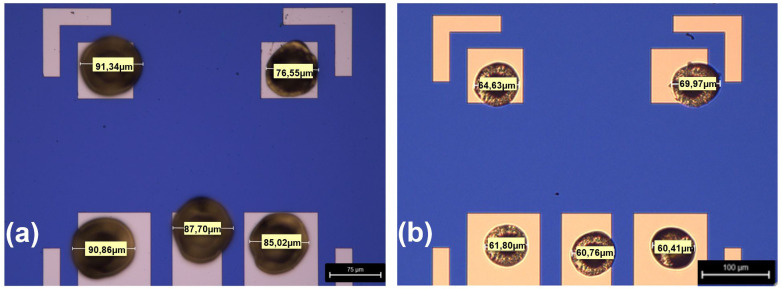
In addition to the bond parameters, the ball size also depends on the diameter of the wire used in the bonding process. The initially used gold wire had a diameter of 25 µm, which produced comparatively large stud bumps, because the ball size will never be smaller than approximately three times the wire size. This often led to long tails and short circuits between the narrow CPW lines. For this reason, the wide wire was replaced with a thinner gold wire (diameter of 17 µm). As shown in Figure 1 (as a typical example), the diameter of the gold stud bumps was significantly reduced after the wire exchange and parameter optimization, yielding a reduction of the size of the stud bumps around 25%. Due to the smaller size of the stud bumps, the risk of short circuits during the flip chip process was avoided completely for the given dimensions of the three lower contact pads shown in Figure 1. Here, the important dimensions are the width of the center contact pad (73 µm) and the gap between the center contact pad and the contact pads on both sides (30 µm). Obviously, a decrease of these dimensions, increases the risk of shorts. A mean size of the bumps of (63.8 ± 3.4) µm was determined by analyzing 60 Au-bumps. This average bump size is slightly smaller than described in 14 65…80 µm and slightly larger than in 15 nearly 45 µm. The optimal bond parameters were determined by slightly varying each individual parameter and checking the diameter of the gold stud bumps. By applying the following bond parameters, a very good yield of the stud bumps of nearly 100% was obtained: ultra-sonic power 100 mW, Electronic Flame-Off (EFO) power 90%, bond-time 150 ms, bond-power 12 cN, chuck-temperature 40°C, tool-temperature 160°C. In contrast to 5, 14 “long” tails (causing shorts) could be avoided completely too.

Figure 1.

Figure 1.

Typical microscope image of the size of the gold stud bumps ( a) before optimization (25 µm diameter of the gold wire) and ( b) after optimization (17 µm diameter of the gold wire). The dimension of each ball is labeled.

3. Flip-chip procedure of PDs and mounting of sleeves

After optimization of the stud bumps, the photodiodes were flip-chip mounted using the flip-chip machine (Finetech Fineplacer Sigma). Several custom-designed and changeable tooltips are available, which are suited for different chip sizes and geometries. Firstly, the miniature PD was picked up by the tool tip in face-down configuration. Afterwards, the gold pads of the PD and the gold stud bumps on the carrier chip were aligned by using two overlaid microscope images of the flip-chip machine. A thermocompression flip-chip process was then applied. In the thermocompression bonding, usually two metals (in our case gold) are joined by applying a constant force at a raising temperature. To achieve less bump deformation, a bonding force of 4 N or 5 N 5, 14, 16 for the 5 pads (each with one bump) was used. This bonding force range was selected based on prior optimization experiments, where various bonding forces were tested, and it was observed that forces between 4 N and 5 N resulted in the least deformation of the stud bumps, ensuring reliable bonding without compromising the integrity of the photodiode or the carrier chip and without causing short circuits. During this process, the temperature gradually increased up to 250°C within a time of 5 s, stayed at 250°C for about 60 s and then reduced to 100°C within a time of 150 s. No underfill glue was needed for this process.

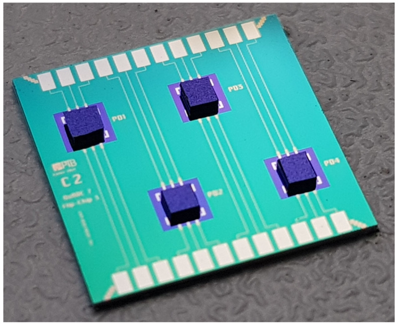
To optimize the flip-chip parameters (bonding force, force/temperature ramp, bump alignment, bump tails) and to estimate the yield of the mounted chips, on-chip test structures were fabricated. The silicon substrate (shown in Figure 2) has four identical simple circuits each consisting of three extended gold lines. The dummy chips, which simply connect the interrupted gold lines of the substrate with each other, were mounted on the test substrate using flip-chip technology. These mounted chips were on-chip electrically characterized (DC measurements) by a wafer prober at 300 K and in a liquid Helium dewar at 4 K. The main purpose for this measurement was to check the electrical connections resulting from the flip-chip process, especially after cooling down to 4 K. The measured results showed that all 4 mounted dummy chips behave as expected (yield 100%, see next section for the yield for mounting many PDs). All opposite lines are connected via the dummy chip, no short circuit between two adjacent lines could be detected, and no degradation was observed after repeated thermal cycling between 300 K and 4 K. While the electrical DC measurements give an indication of the electrical connection they do not fully eliminate the possibility of cracks in the connection interface after cool down and warm up. We have not made any cross section SEM image of the connection after thermal cycling, but we have tested the high-frequency connection of the flip-chip-mounted PDs after thermal cycling, which is briefly commented on further below.

Figure 2. Optical photograph of four dummy chips (size: 350 µm × 350 µm) successfully mounted on the silicon substrate using flip-chip technology.

Figure 2.

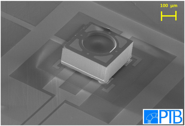
After successfully mounting and testing the electrical connections of the dummy chips, we have started to mount real PDs using the aforementioned technique. Since then, many PDs were mounted onto different chip substrates. We also investigated our mounted chips under a Scanning Electron Microscope (SEM). The SEM image of Figure 3 displays that the mounted PDs were attached nicely to the gold stud bumps underneath. No tilt or twist of the PDs was observed. After optimization of the flip-chip procedure we achieved a yield better than 95% for a total of more than 250 mounted PDs. 95% out of 250 PDs yields approximately 13 PD which were not working. Typically, we mount 2 PDs on each device. In the worst case, i.e., from 125 devices only 13 devices were not fully functional. A device with one working PD is still operational, but in combination with the JAWS chip, only a unipolar waveform can be synthesized. So far, no PD has been destroyed during or after the flip chip procedure. No PD got detached due to repeated thermal cycling between 300 K and 4 K. No critical delamination/failure due to mechanical stress occurred during thermal cycling of the devices, because between the PD and the carrier chip only Au interfaces are used: Au-bond pads on both chips and Au-bumps. We did some preliminary mechanical stress test to remove the sleeves and PDs from the carrier chip. No sleeve or PDs dropped off without introducing some external force. Short circuit of the PDs occurred only occasionally due to the unideal placement of the gold stud bumps. We also comment on the electrical connection of the PDs as mentioned in the previous paragraph. We have performed high-speed measurements using electro-optic sampling of ultrafast voltage pulses generated from optical excitation of the PDs using femtosecond lasers 17 . Even after several cool-down and warm-up cycles we always measured the same PD response, proving that we have proper high-frequency flip-chip connections even after several thermal cycles. This high yield is required due to the relatively high costs of the high-performance PDs and shows that the established flip-chip technology is very robust and reliable.

Figure 3. Tilted SEM image of a PD mounted onto a high-frequency line on a silicon substrate.

Figure 3.

The integrated lens on the backside of the PD is clearly visible.

The employed PDs need to be illuminated from their backside and have an additional integrated lens in their substrate. To connect the optical fiber to the backside-lensed PDs, special fiber sleeves need to be mounted and glued on the carrier chip as precisely as possible. To align the sleeves under the microscope, alignment circles were fabricated on the chip. In the chip designs, the inner diameter of the circles, which are electrically passive, were perfectly matched to the outer diameter of the sleeves.

For flip-chip bonding of the sleeves a specially designed and fabricated sleeve tooltip was installed to the flip-chip machine. The sleeve with a length of 7 mm was picked up by the tooltip and was aligned to the alignment circle by using the two overlaid microscope images of the flip-chip machine. Then a small amount of Stycast 12661 epoxy glue (mixing ratio of Part A to Part B was approximately 1 to 0.28) was applied carefully on the chip substrate. Afterwards, the mounting step started, and the sleeve was carefully lowered by the tooltip and placed on the alignment circle of the substrate. Lastly, to harden the glue, the mounted chips were cured at room temperature for 24 hours and then baked at 80°C for 2 hours, as recommended in the datasheet of the glue.

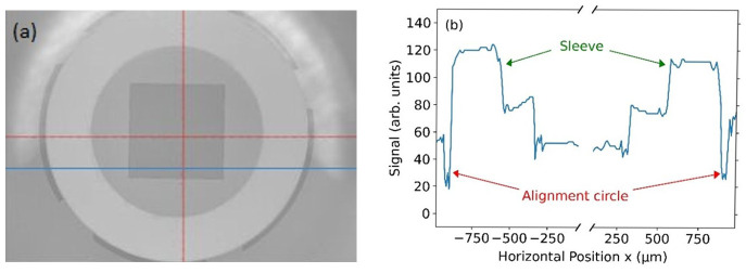
Figure 4 shows an optical photograph of two sleeves being glued onto the chip substrate using the aforementioned process. In order to determine the alignment uncertainty, we analyzed several microscope images, as shown in Figure 5(a). An intensity analysis of the images (see Figure 5b) allowed us to quantitatively determine the standard uncertainty of the alignment procedure. To this end, we extracted the measured width of both alignment circles shown in Figure 5(b) and found that the widths differs by less than 15 μm (in each direction). Since we have no specific knowledge about the distribution function for different cross-sections and different images, we assume a uniform distribution according to 18. This yields a standard uncertainty of the alignment procedure of 15 µm/√3 = 9 µm 18 . At first this number seems to be too large for single-mode fibers with a core diameter below 10 µm. Yet, this accuracy is more than sufficient for our applications, because the active area of the backside lens of the PD has a diameter of 100 µm. To test the quality of the glued sleeves, the chip was repeatedly cooled down and warmed up between 4 K and 300 K. After five cooling-down and warming-up cycles, the mounted sleeves remained stable and stuck firmly onto the chip. We note that five cooling cycles constitute a limited number from which it is impossible to extract a behavior for many more cooling cycles. Yes, we believe that even five cooling cycles without any observed problem denote a very positive trend, which is worth to be reported.

Figure 4. Optical photograph of two sleeves mounted using flip-chip technology and glued to the silicon substrate.
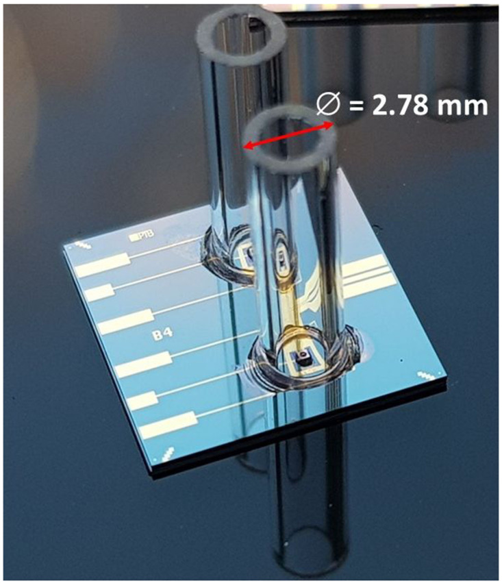
Figure 4.

This photograph was taken before the cool-down. After cooling down there are no visible differences to observe. We note that the sleeve may tilt or shift in alignment if the adhesive is not applied symmetrically with respect to the cross-section of the sleeve. In our experiments we have not observed any tilt or shift in alignment. The sleeves have a length of 7 mm.

Figure 5.

Figure 5.

( a) Microscope image of the sleeve attached to the silicon substrate. On the substrate alignment circles have been fabricated at the positions corresponding to the outer diameter of the sleeve. The red cross just marks the center of the camera image. ( b) Intensity image values in arbitrary units along the blue line in ( a). The alignment circles with a nominal width of 50 µm can be seen at the left- and right-hand side of the plot. The measured width of both alignment circles differs by less than 15 µm, which denotes the alignment accuracy of the sleeve and thus of the fiber-chip coupling. The measured width of both alignment circles is used to extract a standard uncertainty of 9 µm, see main text.

4. Characterization of the mounted PDs

The mounted PDs with and without the sleeves were investigated under Continuous Wave (CW) laser light at room temperature. The CW laser light had a wavelength of 1310 nm, power of 1.6 mW and it was guided onto the backside of the PDs via an optical fiber, which ends in a pigtail ferrule (the glass body of the ferrule was placed directly above the PD). In this case, no sleeve was mounted on the chip. With the help of a positioning table, the chip was moved relative to the ferrule with a step size of 10 µm in the x/y/z direction. Depending on the PD position, the photocurrent of the photodiode was measured and is a measure of the optical coupling. As the ferrule moves away from the optimal alignment position, the photocurrent decreases, indicating reduced optical coupling efficiency. The applied reverse bias of the PD was 4 V. In Figure 6, the measured results show a nice Gaussian like shape with a full width at half maximum of 85 µm. This corresponds very well to the 100 µm diameter of the built-in lens of the PD.

Figure 6. Dependence of the photocurrent of one PD under irradiation by CW laser light with a power of 1.6 mW versus x-y position of the ferrule over the PD.
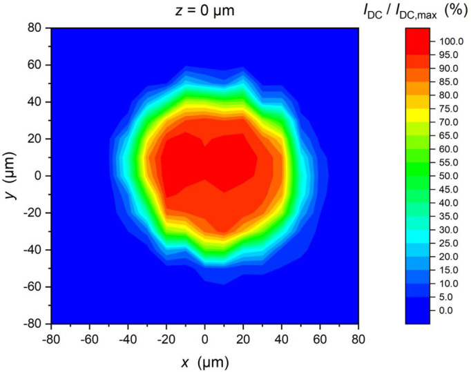
Figure 6.

The measured photocurrent was normalized to I dc (max) = 1.2 mA. The distance of the ferrule to the PD was z = 0 µm.

Next, the mounted PDs together with the glued glass sleeves and attached ferrules were characterized as well. To this end we like to note that we used normal ferrules, without any angles facet. The nominal outer diameter of the ferrules were 1.8 mm with a tolerance of +/- 5 μm, the nominal inner diameter of the sleeve was 1.815 mm. The ferrule end rests directly on the PD substrate. To prevent displacement in the z-direction, the fiber is fixed with light pressure against the PD substrate. As previously mentioned, we have not yet achieved a perfect alignment between the center of the PD and the glass sleeve, with a standard uncertainty below 9 µm. However, as shown in Figure 7, the amplitude of the photocurrent is largely dependent on the rotation angle of the chip with respect to the ferrule and varies between a maximum value and zero. This variation is due to mechanical imperfections, such as scratches on the lens, non-planar contact between the ferrule and lens, imperfect radiation patterns of the ferrule, deviations within the manufacturer's tolerance of the outer diameter of the sleeve and/or the inner diameter of the ferrule along its main axes, and non-cylindrical shapes of the outer diameter of the sleeve and/or the ferrule, which affect the optical coupling efficiency. For a given alignment offset, rotating the fiber slightly adjusts the transition area of light between the ferrule end and the lens, allowing light to couple better to the PD’s active area despite these imperfections. When only considering the standard uncertainty of 9 µm and the built-in lens of the PD with a diameter of 100 µm, we would not expect such a considerable change of the photocurrent. Thus, it is clear that mechanical imperfections of the ferrule-sleeve combination limit the overall coupling efficiency. Two optical fiber-ferrule combinations were tested in the measurement as shown in Figure 6 and studies on other sleeves and ferrules confirm this finding. The asymmetric trend of the green line in Figure 7 is attributed to the differing mechanical imperfections of the two ferrules, which influence the coupling efficiency across different rotation angles. Despite these mechanical imperfections, maximum optical coupling can be obtained by adjusting the rotation angle of the chip and/or the fiber at room temperature and keep it fixed during operation at 4 K. We will perform further investigations on ferrule and sleeves products from different manufacturers to investigate this issue in more detail.

Figure 7. Dependence of the DC output current of one PD under irradiation by CW laser light with a power of 1.6 mW versus rotation angle of the chip with respect to the ferrule.
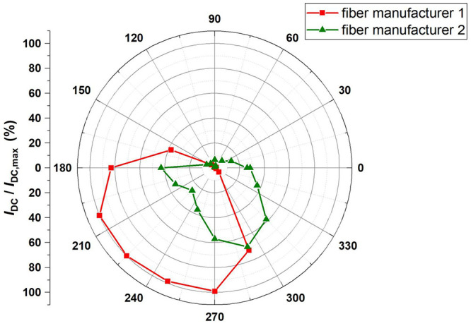
Figure 7.

The measured results were normalized to I dc (max) = 1.2 mA. Two different types of optical fibers were used. They both exhibit a similar behavior.

5. Conclusions

To summarize our work, we successfully established the flip-chip procedure of mounting PDs and glass sleeves at PTB. Our method and statistical analysis support and adds new information to our and our partners previous publications obtained in the framework of different joint projects 5, 10, 13, 14, 16 . After mounting more than 250 PDs with an overall yield better than 95%, this technique has proven to be very reliable and reproducible for our purpose of realizing an multi-channel optical pulse-drive of JAWS chips at low temperatures. We also studied the alignment uncertainty of glass sleeves and ferrules. While the sleeves can be mounted to substrates with a standard uncertainty better than 9 µm, the overall alignment uncertainty of ferrule-sleeves combinations is mainly determined by mechanical imperfections of the two components. In the future, the flip-chip technology will be used at PTB for different applications ranging from optical measurement to quantum technologies.

Ethics and consent

Ethical approval and consent were not required.

Disclaimer

Commercial equipment is identified in this paper to adequately specify the experimental procedure. Such identification does not imply recommendation or endorsement by PTB.

Acknowledgements

The authors would also like to thank T. Weimann, P. Hinze, K. Störr, and R. Gerdau for their technical support and useful discussions.

Funding Statement

This work was partly funded by the EMPIR programme co-financed by the Participating States and from the European Union’s Horizon 2020 research and innovation programme (contract number 20FUN07 SuperQuant) and by the German Federal Ministry of Education and Research (contract number: 13N15934).

The funders had no role in study design, data collection and analysis, decision to publish, or preparation of the manuscript.

[version 2; peer review: 1 approved, 3 approved with reservations]

Data and software availability

Underlying data

Open Access Repository of the Physikalisch-Technische Bundesanstalt: Development of Flip-Chip Technology for the Optical Drive of Superconducting Circuits. https://doi.org/10.7795/720.20240226 19 .

Data are available under the terms of the Creative Commons Attribution 4.0 International license (CC-BY 4.0).

References

  • 1. Tummala RR: Fundamentals of microsystems packaging. Book New York: McGraw-Hill,2001. Reference Source [Google Scholar]
  • 2. Gupta KC, Garg R, Chadha R: Computer-aided design of microwave circuits. Book Artech House Inc.,1981;212. Reference Source [Google Scholar]
  • 3. Gong L, Xu Y-P, Ding B, et al. : Thermal management and structural parameters optimization of MCM-BGA 3D package model. Int J Therm Sci. 2020;147: 106120. 10.1016/j.ijthermalsci.2019.106120 [DOI] [Google Scholar]
  • 4. Brinlee S, Popelar S: A physics-of-failure investigation of flip chip reliability based on lead-free solder fatigue modeling. J Microelectron Electron Packag. 2023;20(1):27–35. 10.4071/001c.74728 [DOI] [Google Scholar]
  • 5. Bardalen E, Karlsen B, Malmbekk H, et al. : Packaging and demonstration of optical-fiber-coupled photodiode array for operation at 4 K. IEEE Trans Comp Pack Manuf Technol. 2017;7(9):1395–1401. 10.1109/TCPMT.2017.2699485 [DOI] [Google Scholar]
  • 6. Di Cino M, Li F: Flip chip die-to-wafer bonding review: gaps to high volume manufacturing. Semiconductor Science and Information Devices. 2022;4(1). 10.30564/ssid.v4i1.4474 [DOI] [Google Scholar]
  • 7. Kieler O, Behr R, Wendisch R, et al. : Towards a 1 V Josephson arbitrary waveform synthesizer. IEEE Trans Appl Supercond. 2015;25(3): 1400305. 10.1109/TASC.2014.2366916 [DOI] [Google Scholar]
  • 8. Kieler O, Wendisch R, Gerdau R, et al. : Stacked Josephson junction arrays for the pulse-driven AC Josephson voltage standard. IEEE Trans Appl Supercond. 2021;31(5): 1100705. 10.1109/TASC.2021.3060678 [DOI] [Google Scholar]
  • 9. Flowers-Jacobs NE, Rüfenacht A, Fox A, et al. : Development and applications of a four-volt Josephson arbitrary waveform synthesizer. IEEE International Superconductive Electronics Conference (ISEC). Riverside, CA, USA,2019;1–2. 10.1109/ISEC46533.2019.8990937 [DOI] [Google Scholar]
  • 10. Kieler O, Karlsen B, Ohlckers P, et al. : Optical pulse-drive for the pulse-driven AC Josephson voltage standard. IEEE Trans Appl Supercond. 2019;29(5): 1200205. 10.1109/TASC.2019.2899851 [DOI] [Google Scholar]
  • 11. Herick J, Palafox L, Bardalen E, et al. : Realization of an opto-electronic bias for pulse-driven Josephson voltage standards at PTB. CPEM Conference. Denver, USA,2020;1–2. 10.1109/CPEM49742.2020.9191913 [DOI] [Google Scholar]
  • 12. Brevik J, Lee D, Fox A, et al. : Bipolar waveform synthesis with an optically driven Josephson arbitrary waveform synthesizer. IEEE Trans Appl Supercond. 2022;32(9): 1400408. 10.1109/TASC.2022.3167660 [DOI] [Google Scholar]
  • 13. Karlsen B, Bardalen E, Nissilä J, et al. : High-speed pulsation of a cryogenically operable bipolar photodiode module for the Josephson arbitrary waveform synthesizer. CPEM Conference. Denver, USA,2020. 10.1109/CPEM49742.2020.9191751 [DOI] [Google Scholar]
  • 14. Bardalen E: Reliable packaging and development of photodiode module for operation at 4 K. Dissertation, University of South-Eastern Norway,2018. Reference Source
  • 15. Li K, Xu G, Zhao W, et al. : Golden bump based flip-chip interconnection for superconducting multi-chip module. IEEE Trans Appl Supercond. 2023;33(5): 1200106. 10.1109/TASC.2023.3263132 [DOI] [Google Scholar]
  • 16. Bardalen E, Karlsen B, Malmbekk H, et al. : Reliability study of fiber-coupled photodiode module for operation at 4 K. Microelectron Rel. 2018;81:362–367. 10.1016/j.microrel.2017.10.034 [DOI] [Google Scholar]
  • 17. Priyadarshi S, Tian H, Fernandez Scarioni A, et al. : Cryogenic fiber-coupled electro-optic characterization platform for high-speed photodiodes. J Infrared Milli Terahz Waves. 2024;45:159–170. 10.1007/s10762-024-00966-1 [DOI] [Google Scholar]
  • 18. BIPM, IEC, IFCC et al. : Evaluation of measurement data — guide to the expression of uncertainty in measurement. Joint Committee for Guides in Metrology, JCGM, 100: 2008. Reference Source [Google Scholar]
  • 19. Kieler O, Tian H, Kraus M, et al. : Development of flip-chip technology for the optical drive of superconducting circuits. Hosting Institution: Physikalisch-Technische Bundesanstalt (PTB), [Dataset]. 10.7795/720.20240226 [DOI] [PMC free article] [PubMed]
Open Res Eur. 2024 Dec 5. doi: 10.21956/openreseurope.20301.r46241

Reviewer response for version 2

Ming-Han Chou 1

The manuscript authored by O. Kieler et al. presents the development of a gold stud bump-based flip-chip technology for integrating photodiodes and fibers with superconducting circuits. The authors provide detailed descriptions of the fabrication process, optimize the bump geometry, and evaluate the integrated devices at both room and cryogenic temperatures. They demonstrate a high fabrication yield and offer a thorough characterization of device performance, including an analysis of misalignment effects.

Although gold bump integration techniques are well-documented in the literature, this manuscript stands out by providing detailed fabrication protocols that could enable other research groups to reproduce their results. This contribution is therefore a valuable addition to the field.

As many key points have already been addressed in other reviewers' comments and the authors have provided satisfactory responses in the revised manuscript (version 2), I have the following remaining comments and minor suggestions:

  1. The authors validate the yield rate by testing DC connections at cryogenic temperatures. Have they conducted any microwave measurements, such as S11 or S21, to assess the stability of the device under high-frequency signals? If the microwave performance remains consistent after multiple cooling cycles, it would further enhance the potential applications of this fabrication process in quantum technologies.

  2. The authors attribute the limited coupling efficiency to imperfections in the ferrule-sleeve integration. Given this limitation, what was the rationale behind selecting this method for coupling the fiber to the photodiode? A discussion addressing this choice would provide helpful context for readers.

  3. In Figure 7, the statement "They both exhibit a similar behavior" appears inaccurate, as the coupling efficiencies for the two fibers differ significantly.

Overall, the manuscript is clearly written and easy to follow. Once the authors address the questions above, I support the indexing the manuscript.

Is the rationale for developing the new method (or application) clearly explained?

Yes

Is the description of the method technically sound?

Yes

Are the conclusions about the method and its performance adequately supported by the findings presented in the article?

Yes

If any results are presented, are all the source data underlying the results available to ensure full reproducibility?

Yes

Are sufficient details provided to allow replication of the method development and its use by others?

Yes

Reviewer Expertise:

Quantum acoustics, hybrid quantum systems, superconducting circuits, fabrications

I confirm that I have read this submission and believe that I have an appropriate level of expertise to confirm that it is of an acceptable scientific standard, however I have significant reservations, as outlined above.

Open Res Eur. 2024 Nov 23. doi: 10.21956/openreseurope.20301.r46093

Reviewer response for version 2

Jie Ren 1

The author answered all my questions and made some modifications and additions to the manuscript. I believe this can be indexed as a method article.

Is the rationale for developing the new method (or application) clearly explained?

Partly

Is the description of the method technically sound?

Partly

Are the conclusions about the method and its performance adequately supported by the findings presented in the article?

Partly

If any results are presented, are all the source data underlying the results available to ensure full reproducibility?

No source data required

Are sufficient details provided to allow replication of the method development and its use by others?

No

Reviewer Expertise:

SFQ circuit design, low-temperature measurement

I confirm that I have read this submission and believe that I have an appropriate level of expertise to confirm that it is of an acceptable scientific standard.

Open Res Eur. 2024 Jun 27. doi: 10.21956/openreseurope.18891.r41246

Reviewer response for version 1

Jie Ren 1

This article introduces the gold stud bump-based flip-chip technology applied in optical-driven superconducting circuits. The research and development of flip-chip and optical pulse drive technology for superconducting circuits were mainly discussed, with a focus on the process of installing photodiodes and fiber optic sleeves on silicon substrates. And certain verification was carried out in the process of flip soldering. The highly reliable packaging of low-temperature chips is a recent research hotspot. There have been some reports on the packaging of low-temperature superconducting chips using gold bumps (such as 1. R. Das et al., "Interconnect Scheme for Die-to-Die and Die-to-Wafer-Level Heterogeneous Integration for High-Performance Computing," 2019 IEEE 69th Electronic Components and Technology Conference (ECTC), Las Vegas, NV, USA, 2019, pp. 1611-1621, doi: 10.1109/ECTC.2019.00248 and 2. K. Li  et al., "Golden Bump Based Flip-Chip Interconnection for Superconducting Multi-Chip Module," in  IEEE Transactions on Applied Superconductivity, vol. 33, no. 5, pp. 1-6, Aug. 2023, Art no. 1200106, doi: 10.1109/TASC.2023.3263132.). The packaging technology demonstrated in this paper have not shown significant advantages and innovations compared to existing works. Therefore, it is recommended to consider whether it is suitable for indexed after major revision. Some specific suggestions are as follows:

1. Please clearly explain the innovation of the gold-stud-bump-based flip-chip packaging technology in this article.

2. The article mentions that changing the wire can intuitively obtain the change in the diameter of the protrusion, but by adjusting the protrusion preparation parameters, 25 μ m wire should also be able to achieve a preparation effect of nearly equivalent nail head protrusion diameter for 17 μ m wire. In ref K. Li et al., "Golden Bump Based Flip-Chip Interconnection for Superconducting Multi-Chip Module," in IEEE Transactions on Applied Superconductivity, vol. 33, no. 5, pp. 1-6, Aug. 2023, Art no. 1200106, doi: 10.1109/TASC.2023.3263132., it is possible to achieve a diameter of approximately 2.2 times the diameter of the gold wire. This data is far superior to the results of this article.

3. The gold bump prepared by the nail head method will retain a certain amount of tail wire, and the gold bump maintains a certain hardness. When the tail wire length is different, will it affect the selection of bonding parameters?

4. The article mentioned that the test results showed no failure was found after multiple thermal cycles of flip soldering, which means that the yield rate was 100% after both electrical and thermal cycles, but no detailed testing data was provided, please add them.

5. It can be seen that no phenomenon of open circuit or short circuit under DC testing after the structural interconnection undergoes thermal cycling However, it cannot fully explain whether there are cracks or other effects on the connection interface after low-temperature cycling at the bump, I believe it is necessary to characterize the cross-section at the bump interface to check this.

6. After flip soldering, the photodiode and fiber optic sleeve of the chip undergo five cooling and preheating cycles between 4 K and 300 K, and the sleeve remains stable. However, the number of 5 cycles is too small. It is recommended to increase the number of experiments. In addition, it is recommended to increase the verification of shear force to quantify the verification effect.

7. The fiber optic sleeve fixed with Stycast 12661 adhesive did not show any looseness or damage after undergoing temperature cycling, but the CTE of epoxy resin differs significantly from that of other components. Will different expansion and deformation situations cause the sleeve to tilt or shift in alignment, which will affect the subsequent fiber optic connection?

8. More details should be provided when explaining the results shown in Figure 7. For instance, what is the temperature the measurement carries out? what is the diameter of the ferrules and how is it compared to that of the glass sleeves? And what is the distance between the fiber end and the integrated lens on the backside of the PD?

9. The unideal results in Figure 7 are attributed to the mechanical imperfections. My question is what kind of mechanical imperfections are causing these and how?

Is the rationale for developing the new method (or application) clearly explained?

Partly

Is the description of the method technically sound?

Partly

Are the conclusions about the method and its performance adequately supported by the findings presented in the article?

Partly

If any results are presented, are all the source data underlying the results available to ensure full reproducibility?

No source data required

Are sufficient details provided to allow replication of the method development and its use by others?

No

Reviewer Expertise:

SFQ circuit design, low-temperature measurement

I confirm that I have read this submission and believe that I have an appropriate level of expertise to state that I do not consider it to be of an acceptable scientific standard, for reasons outlined above.

References

  • 1. Interconnect Scheme for Die-to-Die and Die-to-Wafer-Level Heterogeneous Integration for High-Performance Computing. IEEE .2019;
  • 2. Golden Bump Based Flip-Chip Interconnection for Superconducting Multi-Chip Module. IEEE .2023;
Open Res Eur. 2024 Oct 15.
Oliver Kieler 1

This article introduces the gold stud bump-based flip-chip technology applied in optical-driven superconducting circuits. The research and development of flip-chip and optical pulse drive technology for superconducting circuits were mainly discussed, with a focus on the process of installing photodiodes and fiber optic sleeves on silicon substrates. And certain verification was carried out in the process of flip soldering. The highly reliable packaging of low-temperature chips is a recent research hotspot. There have been some reports on the packaging of low-temperature superconducting chips using gold bumps (such as 1. R. Das et al., "Interconnect Scheme for Die-to-Die and Die-to-Wafer-Level Heterogeneous Integration for High-Performance Computing," 2019 IEEE 69th Electronic Components and Technology Conference (ECTC), Las Vegas, NV, USA, 2019, pp. 1611-1621, doi: 10.1109/ECTC.2019.00248 and 2. K. Li et al., "Golden Bump Based Flip-Chip Interconnection for Superconducting Multi-Chip Module," in IEEE Transactions on Applied Superconductivity, vol. 33, no. 5, pp. 1-6, Aug. 2023, Art no. 1200106, doi: 10.1109/TASC.2023.3263132.). The packaging technology demonstrated in this paper have not shown significant advantages and innovations compared to existing works. Therefore, it is recommended to consider whether it is suitable for indexed after major revision. Some specific suggestions are as follows:

Comment: 1. Please clearly explain the innovation of the gold-stud-bump-based flip-chip packaging technology in this article.

Response: Please see comment 4 of the second reviewer for an answer and corresponding changes to the manuscript.

Comment: 2. The article mentions that changing the wire can intuitively obtain the change in the diameter of the protrusion, but by adjusting the protrusion preparation parameters, 25 μ m wire should also be able to achieve a preparation effect of nearly equivalent nail head protrusion diameter for 17 μ m wire. In ref K. Li et al., "Golden Bump Based Flip-Chip Interconnection for Superconducting Multi-Chip Module," in IEEE Transactions on Applied Superconductivity, vol. 33, no. 5, pp. 1-6, Aug. 2023, Art no. 1200106, doi: 10.1109/TASC.2023.3263132., it is possible to achieve a diameter of approximately 2.2 times the diameter of the gold wire.

Response: This data is far superior to the results of this article. We thank the reviewer for mentioning this article and agree that it needs to be cited. We added the mentioned reference and extended the sentence at the end of Section 2: “This average bump size is slightly smaller than described in [14] 65…80 µm and slightly larger than in [15] nearly 45 µm.”.

​​​​​​​Comment: 3. The gold bump prepared by the nail head method will retain a certain amount of tail wire, and the gold bump maintains a certain hardness. When the tail wire length is different, will it affect the selection of bonding parameters?

Response: The tail length was optimized to be as short as possible, because a long tail will result in a large effective area of the bump after coining and flip-chip, which will directly increase the probability of shorts between the signal and ground lines of the CPW. Please see comment 1 of the first reviewer for a further answer and corresponding changes to the manuscript.

​​​​​​​Comment: 4. The article mentioned that the test results showed no failure was found after multiple thermal cycles of flip soldering, which means that the yield rate was 100% after both electrical and thermal cycles, but no detailed testing data was provided, please add them.

Response: To us it is not fully clear what the reviewer exactly means with “testing data” and “electrical ...cycles” (e.g., DC resistance before and after cool down, optical photographs, ...). In this regard we refer to Fig. 4, where we changed the caption by adding the statement: “This photograph was taken before the cool-down. After cooling down there are no visible differences to observe.” Additionally, we like to refer to the next comment and answer, where we mention high-frequency measurements for subsequent cool-downs.

​​​​​​​Comment: 5. It can be seen that no phenomenon of open circuit or short circuit under DC testing after the structural interconnection undergoes thermal cycling. However, it cannot fully explain whether there are cracks or other effects on the connection interface after low-temperature cycling at the bump, I believe it is necessary to characterize the cross-section at the bump interface to check this.

Response: We have removed some PD after flip chip bonding and cool down cycles and inspected the remaining surface of the chip and the PD optically. No indication of cracks could be found. We agree that this optical inspection is different than SEM or even TEM measurements, which are, however, beyond the scope of this manuscript. In addition we have performed high-speed measurements using electro-optic sampling of ultrafast voltage pulses generated by the photodiode  on several samples [ https://doi.org/10.1007/s10762-024-00966-1]. This corresponds to RF testing instead of DC testing. From these measurements it is clear that we remain to have proper high-frequency connections even after multiple cool down cycles. We have added corresponding remarks to Section 3: “While the electrical DC measurements give an indication of the electrical connection they do not fully eliminate the possibility of cracks in the connection interface after cool down and warm up. We have not made any cross section SME image of the connection after thermal cycling, but we have tested the high-frequency connection of the flip-chip-mounted PDs after thermal cycling, which is briefly commented on further below. ” and “We also comment on the electrical connection of the PDs as mentioned in the previous paragraph. We have performed high-speed measurements using electro-optic sampling of ultrafast voltage pulses generated from optical excitation of the PDs using femtosecond lasers [17]. Even after several cool-down and warm-up cycles we always measured the same PD response, proving that we have proper high-frequency flip-chip connections even after several thermal cycles.”.

​​​​​​​Comment: 6. After flip soldering, the photodiode and fiber optic sleeve of the chip undergo five cooling and preheating cycles between 4 K and 300 K, and the sleeve remains stable. However, the number of 5 cycles is too small. It is recommended to increase the number of experiments. In addition, it is recommended to increase the verification of shear force to quantify the verification effect.

Response: We thank the reviewer for this comment. Of course every study can be extended and we agree that the number repetitive cycles is limited. Yet, we believe that even after 5 cycles a certain trend can be obtained. We have therefore left the number of cycles unchanged, but added a corresponding remark to Section 3: “We note that five cooling cycles constitute a limited number from which is it impossible to extract a behaviour for 20 or more cooling cycles. Yes, we believe that even five cooling cycles without any observed problem denote a very positive trend which is worth to be reported.”.

​​​​​​​Comment: 7. The fiber optic sleeve fixed with Stycast 12661 adhesive did not show any looseness or damage after undergoing temperature cycling, but the CTE of epoxy resin differs significantly from that of other components. Will different expansion and deformation situations cause the sleeve to tilt or shift in alignment, which will affect the subsequent fiber optic connection?

Response: We believe that such a situation might happen, in particular, if the adhesive is not applied symmetrically with respect to the cross-section of the sleeve. In our experiments we have not observed any tilt or shift in alignment. We have added a corresponding sentence to the caption of Figure 4.

​​​​​​​Comment: 8. More details should be provided when explaining the results shown in Figure 7. For instance, what is the temperature the measurement carries out? what is the diameter of the ferrules and how is it compared to that of the glass sleeves? And what is the distance between the fiber end and the integrated lens on the backside of the PD?

Response: The measurements were carried out at room temperature. The nominal outer diameter of the ferrule was 1.8 mm with a tolerance of +/- 5 μm, the nominal inner diameter of the sleeve was 1.815 mm. The ferrule end rests directly on the PD substrate. To prevent displacement in the z-direction, the fiber is fixed with light pressure against the PD substrate. This explanation was directly adopted in Section 4. The main point that we want to make with Fig. 7 is that despite the mechanical imperfections, maximum optical coupling can be obtained by adjusting the rotation angle of the chip and/or the fiber at room temperature and keep it fixed during operation at 4 K.

​​​​​​​Comment: 9. The unideal results in Figure 7 are attributed to the mechanical imperfections. My question is what kind of mechanical imperfections are causing these and how?

​​​​​​​ Response: Please see comment 5 of the first reviewer for a further answer and corresponding changes to the manuscript.

Open Res Eur. 2024 Jun 26. doi: 10.21956/openreseurope.18891.r41237

Reviewer response for version 1

Saif Wakeel 1

Your Report

The authors extended the use of flip-chip technology for bonding photodiodes and fiber sleeves. I have following comments/revision request before proceeding to next stage. 

  1. Effective thermal management is crucial to prevent overheating, especially in high-power applications. Despite these advantages, the flip-chip process is more complex than wire bonding, requiring precision alignment and careful control of the soldering process.   Reference required..

  2. The reliability of flip-chip assemblies is influenced by factors such as solder joint integrity and underfill material properties. If the flip-chip assembly is aimed for operation at cryogenic temperatures, the challenges further increase, as the thermal expansion of the different materials must be considered. .. Reference required

  3. Showing complexity of flip chip packaging doesn't look relevant with the current study. If flip chip is that complex then why authors are using it?

  4. The second paragraph lists the literature one by one but novelty of paper is not clearly mentioned...

  5. Due to the smaller size of the stud bumps, the risk of short circuits during the flip chip process was avoided completely. A mean size of the bumps of (63.8 ± 3.4) µm was determined by analyzing 60 Au-bumps. Is there a mathematical relation between the bump size and stud bump size to avoid short circuiting?

  6. To achieve less bump deformation, a bonding force of 4 N or 5 N11–13 for the 5 pads (each with one bump) was used . Do you think increasing pressure may expect the chances of short circuit as solder can spread more?

  7. What is the effect of changing temperature on delamination? Or shear strength of device? It could be good to include those. While doing thermal cycling thermo-mechanical stresses are generated which result in delamination/failure of devices?

  8. After optimization of the flip-chip procedure we achieved a yield better than 95% for a total of more than 250 mounted PDs. Can author comment or make a table with how many devices were successful and how many failures?

  9. Figure 3. Tilted SEM image of a PD mounted onto a high-frequency line on a silicon substrate. To observe delamination, it could be good to do cross section and show bonded interface.

  10. After five cooling-down and warming-up cycles, the mounted sleeves remained stable and stuck firmly onto the chip. Do you have any zoom in microscopic image to show this?

  11. Figure 4. Optical photograph of two sleeves mounted using flip-chip technology and glued to the silicon substrate. Is this image before cool down or after cool down?

  12. When only considering the accuracy of 15 µm and the built-in lens of the PD with a diameter of 100 µm. Is this alignment accuracy or alignment tolerance in both cases shouldn't it be with plus minus sign if they are in both positive and negative directions?

Is the rationale for developing the new method (or application) clearly explained?

Partly

Is the description of the method technically sound?

Yes

Are the conclusions about the method and its performance adequately supported by the findings presented in the article?

Yes

If any results are presented, are all the source data underlying the results available to ensure full reproducibility?

Yes

Are sufficient details provided to allow replication of the method development and its use by others?

Partly

Reviewer Expertise:

Photonic packaging, electronic packaging, flip-chip technology, reliability of photonic and electronic devices, wafer-scale assembly or bonding of devices.

I confirm that I have read this submission and believe that I have an appropriate level of expertise to confirm that it is of an acceptable scientific standard, however I have significant reservations, as outlined above.

Open Res Eur. 2024 Oct 15.
Oliver Kieler 1

The authors extended the use of flip-chip technology for bonding photodiodes and fiber sleeves. I have following comments/revision request before proceeding to next stage.

Reviewer comment:  Effective thermal management is crucial to prevent overheating, especially in high-power applications. Despite these advantages, the flip-chip process is more complex than wire bonding, requiring precision alignment and careful control of the soldering process.  Reference required.

Author response: We agree with the referee and added the following reference to Section 1 after the sentence “Effective thermal management is crucial to prevent overheating, especially in high-power applications.”: Gong, L.; Xu, Y.-P.; Ding, B.; Zhang, Z.-H.; Huang,  Z.-Q.;  Thermal management and structural parameters optimization of MCM-BGA 3D package model, Int. J. Therm. Sci., 2020, vol. 147, Art. no. 106120, https://doi.org/10.1016/j.ijthermalsci.2019.106120. 2.  

Reviewer comment: The reliability of flip-chip assemblies is influenced by factors such as solder joint integrity and underfill material properties. If the flip-chip assembly is aimed for operation at cryogenic temperatures, the challenges further increase, as the thermal expansion of the different materials must be considered. .. Reference required

Author response: We agree with the referee and shifted the former reference [12] to the end of the sentence “The reliability of flip-chip assemblies is influenced ... as the thermal expansion of the different materials must be considered.” in Section 1, with the new reference number [5]. Moreover, we added the following reference to Section 1 after the sentence “Despite these advantages, the flip-chip process is more complex than wire bonding, requiring precision alignment and careful control of the soldering process.”: Brinlee, S. and Popelar, S.; A physics-of-failure investigation of flip chip reliability based on lead-free solder fatigue modeling, J. Microelectron. Electron. Packag., 2023, vol. 20(1): 27–35, https://doi.org/10.4071/imaps.1939648.   

Reviewer comment: Showing complexity of flip chip packaging doesn't look relevant with the current study. If flip chip is that complex then why authors are using it?

Author response: Using the tiny (350 µm × 350 µm) photodiodes a packaging method other than flip-chip/chip-on-chip/pick-and-place is hardly possible. Due to the backside illuminated PD configuration, the flip-chip is the first and from our point of view probably the only choice. We have added the following sentence to Section 1 to clarify this issue: “We like to note that due to the properties of the PDs, which are discussed in more detail further below, flip-chip mounting of the PDs is the most straightforward way of attaching them to a substrate.”

Reviewer comment: The second paragraph lists the literature one by one but novelty of paper is not clearly mentioned...

Author response: The novelty of our work is to combine opto-electronics and superconducting quantum electronics for a particular application, which is the pulse-driven Josephson Arbitrary Waveform Synthesizer (JAWS). Our Method Article also demonstrates that the whole procedure can now be performed at PTB. Since these facts are already described in the plain summary and introduction we have only changed the last sentence of Section 1 to emphasize that this manuscript denotes a Method Article in ORE and not a Research Article.

Reviewer comment: Due to the smaller size of the stud bumps, the risk of short circuits during the flip chip process was avoided completely. A mean size of the bumps of (63.8 ± 3.4) µm was determined by analyzing 60 Au-bumps. Is there a mathematical relation between the bump size and stud bump size to avoid short circuiting?

Author response: No equation was derived, but the combination of position of the bump (related to the center of the PD pad) and the size versus the geometrical dimensions of the CPW (line width and gap between ground and center line) will determine the probability of shorts. We have added the following explanation to Section 2: “... for the given dimensions of the three lower contact pads shown in Fig. 1. Here, the important dimensions are the width of the center contact pad (73 µm) and the gap between the center contact pad and the contact pads on both sides (30 µm). Obviously, a decrease of these dimensions, increases the risk of shorts.”.

Reviewer comment: To achieve less bump deformation, a bonding force of 4 N or 5 N 11–13 for the 5 pads (each with one bump) was used. Do you think increasing pressure may expect the chances of short circuit as solder can spread more?

Author response: Using higher bond force increased the squeezing of the Au bumps and consequently the diameter of the Au bump was increased too. This directly increased the occurrence of shorts, too. In the manuscript this issue has already been addressed, see comment 1 of the first referee and our corresponding answer.

Reviewer comment: What is the effect of changing temperature on delamination? Or shear strength of device? It could be good to include those. While doing thermal cycling thermo-mechanical stresses are generated which result in delamination/failure of devices?

Author response: No critical delamination/failure due to mechanical stress occurs during thermal cycling of the devices, because between the PD and the carrier chip only Au interfaces are used: Au-bond pads on both chips and Au-bumps. This explanation was directly added to Section 3.  

Reviewer comment: After optimization of the flip-chip procedure we achieved a yield better than 95% for a total of more than 250 mounted PDs. Can author comment or make a table with how many devices were successful and how many failures?

Author response: 95% out of 250 PDs yields approximately 13 PD which were not working. Typically, we mount 2 PDs on each device. In the worst case, i.e., from 125 devices only 13 devices were not fully functional. A device with one working PD is still operational, but in combination with the JAWS chip, only a unipolar waveform can be synthesized. This explanation was directly added to Section 3. 

Reviewer comment: Figure 3. Tilted SEM image of a PD mounted onto a high-frequency line on a silicon substrate. To observe delamination, it could be good to do cross section and show bonded interface.

Author response: A cross section image would be indeed good, but this was not performed. We did some preliminary mechanical stress test to remove the sleeves and PDs from the carrier chip. We have added the following sentence to Section 3: “No sleeve or PDs dropped off without introducing some external force.” 

Reviewer comment:  After five cooling-down and warming-up cycles, the mounted sleeves remained stable and stuck firmly onto the chip. Do you have any zoom in microscopic image to show this?

Author response: Unfortunately, we do not have a zoomed image. Yet, we note that after cooling down there are no visible differences to observe. We have added this explanation to the caption of Figure 4. 

Reviewer comment: Figure 4. Optical photograph of two sleeves mounted using flip-chip technology and glued to the silicon substrate. Is this image before cool down or after cool down? This photograph was taken before the cool-down.

Author response: After cooling down there are no visible differences to observe. We have added this explanation to the caption of Figure 4.  13.  

Reviewer comment: When only considering the accuracy of 15 µm and the built-in lens of the PD with a diameter of 100 µm. Is this alignment accuracy or alignment tolerance in both cases shouldn't it be with plus minus sign if they are in both positive and negative directions?

Author response: We thank the reviewer for this remark and agree that our wording is not very clear and should be improved. From Fig. 5(b) we extract a variation of the center of the alignment sleeve being less than 15 µm in each direction. Since we have no specific knowledge about the distribution function of this variation for different cross sections and images, we assume a uniform distribution according to Section 4.3.7 of Ref. [18]. This yields a standard uncertainty of the sleeve alignment procedure of 15 µm/sqrt(3) = 9 µm. Please note that according to Ref. [18] it is not necessary to add a +/- sign when stating standard uncertainties. In the manuscript we have added the following text to Section 3: “An intensity analysis of the images (see Figure 5b) allowed us to quantitatively determine the standard uncertainty of the alignment procedure. To this end, we extracted the measured width of both alignment circles shown in Fig. 5(b) and found that the widths differ by less than 15 μm (in each direction). Since we have no specific knowledge about the distribution function for different cross sections and different images, we assume an uniform distribution according to Ref. [18]. This yields a standard uncertainty of the alignment procedure of 15 µm/ 3 Inline graphic = 9 µm.”. Moreover, we have replaced “accuracy” by “uncertainty” at several places throughout the manuscript and adopted the expression for the standard uncertainty of the sleeve alignment procedure as explained above to be 9 µm. Finally, Ref. [18] has been added.

Open Res Eur. 2024 Jun 11. doi: 10.21956/openreseurope.18891.r40361

Reviewer response for version 1

Zhi Ting Ye 1

The paper proposed the size of the gold stud bumps, and flip-chip parameters were optimized, and the fiber sleeves were aligned with specially fabricated alignment circles before applying thermocompression with the flip-chip machine.  This is interesting research and the writing is smooth.  The author please respond to the following recommendations:

Q1. How were the size of the gold stud bumps and flip-chip parameters optimized to increase the yield and success rate of the flip-chip procedure?

Q2. What were the challenges faced in connecting optical fibers to the photodiodes in an optimal position, and how were they overcome?

Q3. What were the results of testing the mounted photodiodes at both room temperature and cryogenic temperature and how did mechanical imperfections affect the alignment accuracy?

Q4. How does the measured photocurrent of the photodiode under irradiation by CW laser light vary with the x-y position of the ferrule over the PD, as shown in Figure 6, and what does this variation indicate about the optical coupling efficiency in the system?

Q5. In Figure 7, under continuous laser irradiation, how does the DC output current of the photodiode change with the rotation angle of the chip relative to the ferrule? What impact does this change have on the alignment accuracy and optical coupling efficiency in the system?

Also, please explain the reason why the green line trend is asymmetric.

Is the rationale for developing the new method (or application) clearly explained?

Yes

Is the description of the method technically sound?

Yes

Are the conclusions about the method and its performance adequately supported by the findings presented in the article?

Yes

If any results are presented, are all the source data underlying the results available to ensure full reproducibility?

Yes

Are sufficient details provided to allow replication of the method development and its use by others?

Yes

Reviewer Expertise:

high power packaged

I confirm that I have read this submission and believe that I have an appropriate level of expertise to confirm that it is of an acceptable scientific standard, however I have significant reservations, as outlined above.

Open Res Eur. 2024 Oct 15.
Oliver Kieler 1

We appreciate the referees’ efforts made to review our manuscript entitled “Development of flip-chip technology for the optical drive of superconducting circuits”, which we submitted as Method Article to Open Research Europe. In the revised manuscript, we have taken care of the requests and suggestions made by the referees, which we found very helpful to improve our Method Article. The corresponding changes have been highlighted as green text in the revised manuscript. In the following we provide a point-to-point reply to the referees’ comments. For each single point we first provide an answer to the referee and then explain the corresponding changes to the manuscript (if there are any). Reviewer 1: The paper proposed the size of the gold stud bumps, and flip-chip parameters were optimized, and the fiber sleeves were aligned with specially fabricated alignment circles before applying thermocompression with the flip-chip machine.  This is interesting research and the writing is smooth.  The author please respond to the following recommendations:

Q1. How were the size of the gold stud bumps and flip-chip parameters optimized to increase the yield and success rate of the flip-chip procedure?

For optimizing the bond parameters for making the stud bumps, the most significant parameters were slightly varied. It was then checked, whether the diameter of the balls increases or decreases. We finally chose those parameters, where the balls had the smallest diameter and simultaneously “long” tails were avoided. In this way we found the following parameters: ultra-sonic power 100 mW, Electronic Flame-Off (EFO) power 90%, bond-time 150 ms, bond-power 12 cN, chuck-temperature 40°C, tool-temperature 160°C. We added the following sentence to paragraph 2 of Section 2: “The optimal bond parameters were determined by slightly varying each individual parameter and checking the diameter of the gold stud bumps.”. For optimizing the flip-chip bonding process, the most significant parameters were slightly varied again. The change of the size of the stud bumps after the thermocompression bonding was investigated. We chose those parameters, where the size of the stud bumps  increased the least. To reach this goal, we reduced the bonding force to rather low values of 4 N or 5 N. In this way we found the parameters given in the paper. We added the following sentence to Section 3: “This bonding force range was selected based on prior optimization experiments, where various bonding forces were tested, and it was observed that forces between 4 N and 5 N resulted in the least deformation of the stud bumps, ensuring reliable bonding without compromising the integrity of the photodiode or the carrier chip and without causing short circuits.”.

Q2. What were the challenges faced in connecting optical fibers to the photodiodes in an optimal position, and how were they overcome?

One of the main challenges in connecting optical fibers to the photodiodes optimally is to precisely fix the fiber's position to ensure optimal signal coupling. To address this, the glass body of the pigtail ferrule is inserted into a glass sleeve that has been carefully glued directly above the photodiode (PD). This method effectively fixes the fiber's position in the XY plane. However, challenges remain in fine-tuning the rotational angle (θ) and the Z-position. At room temperature, and under continuous wave (CW) light, the optimal angle is determined experimentally. Once identified, the fiber is lightly pressed onto the backside of the PD using a fixture, ensuring the alignment is secure. This method prevents an air gap forming between the PD and the glass ferrule after cooling and ensures that the angle remains correct. By handling these aspects carefully, an optimal connection is achieved that maintains alignment and minimizes signal loss both at room temperature and after cooling to 4 K. Since the above explanation is already given in the text, we have left the manuscript unchanged with respect to this point.

Q3. What were the results of testing the mounted photodiodes at both room temperature and cryogenic temperature and how did mechanical imperfections affect the alignment accuracy?

When the fibers were aligned, mounted, and fixed at room temperature (as described in Q2), the coupling efficiency did not deteriorate after cooling down to liquid helium temperatures. Mechanical imperfections at the fiber end only affected the optimal rotational angle (θ) but did not impact the XY positioning accuracy of the fiber relative to the photodiode. This is because the XY alignment is determined by the precise positioning of the glass sleeve over the photodiode. Thus, the careful initial alignment and mounting ensured stable performance even under cryogenic conditions, with mechanical imperfections playing a minimal role. We changed the following sentence in Section 4: “Thus, it is clear that mechanical imperfections of the ferrule-sleeve combination limit the overall coupling efficiency.”.

Q4. How does the measured photocurrent of the photodiode under irradiation by CW laser light vary with the x-y position of the ferrule over the PD, as shown in Figure 6, and what does this variation indicate about the optical coupling efficiency in the system?

The photocurrent becomes smaller when you leave the focus range of the PD lens, as an increasing proportion of the incident light is not focused on the PD. The range in which this effect occurs can be derived from the data, which also plays a role in the required adjustment accuracy of the sleeve in relation to the center of the lens. Optimum coupling is achieved with an adjustment accuracy of approx. +/- 30 µm in the xy direction in relation to the center of the PD lens, provided that the ferrule end lies planar on the PD lens. We added the following sentence to Section 4: “As the ferrule moves away from the optimal alignment position, the photocurrent decreases, indicating reduced optical coupling efficiency.”.

Q5. In Figure 7, under continuous laser irradiation, how does the DC output current of the photodiode change with the rotation angle of the chip relative to the ferrule? What impact does this change have on the alignment accuracy and optical coupling efficiency in the system?

Also, please explain the reason why the green line trend is asymmetric. Mechanical imperfections (e.g. scratches in the lense, non-planar contact between ferrule and lens, imperfect radiation pattern of the ferrule, deviation within the manufacturer's tolerance of the outer diameter of the ferrule and/or the inner diameter of the sleeve along its main axes, non-cylindrical shapes of the outer diameter of the sleeve and/or the ferrule) affect the optical coupling efficiency. For a given alignment offset between the fiber core and the center of the lens, the transition area of the light from the ferrule end to the lens can be slightly changed by rotating the fiber so that the light coupling into the lens is optimized despite the existence of mechanical imperfections (e.g. scratches in the lens). Since mechanical imperfections are almost unavoidable, the correct angle between the ferrule and lens must be set according to the maximum photocurrent obtained from Figure 7. The behaviour of the green curve is asymmetric due to the different mechanical properties of the employed ferrule as compared to the ferrule used for measuring the red curve. We added the following sentences to Section 4: “This variation is due to mechanical imperfections, such as scratches on the lens, non-planar contact between the ferrule and lens, imperfect radiation patterns of the ferrule, deviations within the manufacturer's tolerance of the outer diameter of the sleeve and/or the inner diameter of the ferrule along its main axes, and non-cylindrical shapes of the outer diameter of the sleeve and/or the ferrule, which affect the optical coupling efficiency. For a given alignment offset, rotating the fiber slightly adjusts the transition area of light between the ferrule end and the lens, allowing light to couple better to the PD’s active area despite these imperfections.”

Associated Data

    This section collects any data citations, data availability statements, or supplementary materials included in this article.

    Data Citations

    1. Kieler O, Tian H, Kraus M, et al. : Development of flip-chip technology for the optical drive of superconducting circuits. Hosting Institution: Physikalisch-Technische Bundesanstalt (PTB), [Dataset]. 10.7795/720.20240226 [DOI] [PMC free article] [PubMed]

    Data Availability Statement

    Underlying data

    Open Access Repository of the Physikalisch-Technische Bundesanstalt: Development of Flip-Chip Technology for the Optical Drive of Superconducting Circuits. https://doi.org/10.7795/720.20240226 19 .

    Data are available under the terms of the Creative Commons Attribution 4.0 International license (CC-BY 4.0).


    Articles from Open Research Europe are provided here courtesy of European Commission, Directorate General for Research and Innovation

    RESOURCES