Abstract
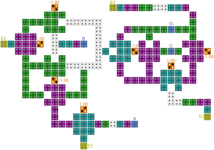
The development of new methods and technologies for improving the stability and reducing the power consumption of electronic devices is a crucial area of research. Quantum-dot Cellular Automata (QCA) has emerged as a promising alternative to the traditional Complementary Metal-Oxide-Semiconductor (CMOS) technology, offering superior optimization in terms of physical size and energy efficiency. This paper introduces three novel digital code converters, designed using the tile-based approach to simplify circuit implementation and enhance integration through optimized majority and inverter gate structures. The proposed converters include: (1) a BCD to gray code converter with 127 cells, 0.18 μm2 occupied area, 3 clock phases, and zero NOT gate achieving a 7.3 % and 100 % reduction in the number of cells and NOT gates, respectively, compared to the most similar design; (2) a BCD to excess-3 code converter with 190 cells, 0.25 μm2 occupied area, 7 clock phases, and 3 NOT gates, showing a 0.5 %, 13.8 %, 41.7 %, and 25 % reduction in cells, area, used clock phases, and NOT gates, respectively, compared to the closest alternative; and (3) a BCD to aiken (2421) code converter with 287 cells, 0.22 μm2 occupied area, zero NOT gate, and 5 clock phases. The energy dissipation for these converters is measured at 55.3 meV, 53.7 meV, and 102 meV, respectively. Simulations are performed using QCADesigner-E version 2.2, validating the functionality and performance of the designs. These results demonstrate the potential of the proposed converters to offer efficient, compact, and low-power solutions for digital systems.
Keywords: Quantum-dot cellular automata, BCD to gray code converter, BCD to excess-3 code converter, BCD to aiken (2421) code converter, Digital code converter
1. Introduction
In the ever-evolving realm of technology, novel methodologies continuously emerge. Among these is Quantum-dot cellular automata (QCA), a promising nanotechnology poised for widespread adoption in future systems and circuits. Presently, while CMOS technology is extensively utilized, it exhibits certain drawbacks, notably circuits with large size and high amount of power consuming. Consequently, researchers and scientists continually seek avenues for improvement, leading to the introduction of QCA technology [1]. Indeed, various practical applications necessitate digital code converters. For example, Binary-Coded Decimal (BCD) forms find utility in ICs acting as seven-segment detector, while Real-Time Clock (RTC) devices store data in format of BCD number. Moreover, gray code facilitates error reduction in specific segments of a Pulse Code Modulation (PCM) system, being very vital in Analog-Digital Converters (ADC). Additionally, excess-3 code finds application in the design of full adders/subtractors in the digital domain. The inception of QCA technology dates back to 1993 when Lent and colleagues first introduced it [2]. QCA boasts numerous advantages, comparing to CMOS, it comes with smaller size and lower amount of power consuming [3]. Code converters are the critical circuits in digital processors among others, because they convert different forms of codes together, such as BCD, aiken, gray, excess-3, etc. codes. Given the diversity of codes utilized in digital systems, the necessity for converter circuits becomes evident, ensuring seamless integration with these systems. Consequently, a range of converter circuits exists, encompassing BCD to excess-3, BCD to gray, BCD to aiken, excess-3 to aiken and etc. [4]. This tool enables users to create innovative components for implementing a wide range of digital circuits, including code converters, thereby optimizing circuits to the fullest extent. For instance, in Ref. [5], a new method called tile-based has been introduced which add the ability of scalability to the designed circuit. In this study, three new converters are designed and simulated utilizing the tile-based method, providing this opportunity to use a unique structure for both majority gate and “NOT gate”. Fouladinia et al. utilized the tile-based method to design and simulate two new circuits converting decimal to excess-3 and vice versa [6]. Raina et al. [7] presented seven distinct circuits for generating a seven-segment code, each deriving from a BCD number. Despite their utility, these circuits were disjointed, suggesting potential for consolidation into a single circuit. Feynman gate, introduced by authors in Ref. [8], facilitated the development of four distinct code converters being binary to gray and binary to excess-3 along with their vice versa circuits converting gray to binary and excess-3 to binary. Similarly, authors in Ref. [9] devised a new NAND gate, termed LTEx module, to develop a binary to gray code converter. Fouladinia and his colleague proposed a new 4-input block being able to implement 4-input comprising “AND”, “NAND”, “OR” and “NOR” gates. They utilized this new block and presented three new converters being decimal to BCD, decimal to excess-3 code and decimal to gray code [10]. In Ref. [11], a novel 5-input majority gate was proposed to construct the gate discussed herein, 8 clock phases were employed, enabling the presentation of a BCD to excess-3 code converter. Furthermore, an exploration of a BCD adder is detailed in Ref. [12]. This BCD adders utilized some circuits which all of them were based on parity preserving logic synthesis. Authors in Ref. [13] utilized a block and presented a multi-code converter converting a decimal number to BCD, gray and excess-3 codes, simultaneously. By introducing an optimized XOR gate, researchers in Ref. [14] designed two distinct converters. While the first circuit of them converted a binary code to excess-3 code, the second one did that for a binary to gray code. In Ref. [15], authors presented two types of converters, binary to gray code and gray code to binary. They have just designed their circuits with gate-based method without introducing new methods or blocks and without applying clocking being an imperative action in QCA circuits. In Ref. [16], the authors introduced a fault-tolerant design for a binary to gray code converter using Quantum-dot Cellular Automata. Their approach incorporates the majority gate, inverter gate, and wire-level cell redundancy to enhance fault tolerance. The proposed circuits were simulated and evaluated using the QCADesigner 2.0.3 software. The study specifically examined the impact of four defect types: missing cells, displacement, misalignment, and the presence of extra cells. Researchers have developed a binary to gray code converter based on QCA technology. The design leverages the Feynman gate as a core component to construct the converter layout. The proposed structure relies on reversible logic to perform the binary to gray code conversion efficiently. To ensure the accuracy of the design, simulations were carried out using QCADesigner version 2.0.3. Additionally, QCAPro software was employed to evaluate the power dissipation of the converter [17]. In Ref. [18], the researchers introduced a QCA-based design for a quantum reversible Fredkin gate. Building on this, they developed both 4-bit and 8-bit binary to gray code converters, along with their inverse, gray to binary converters. The proposed designs were scalable and can be extended to support N-bit conversions. To switch between conversion modes, a 2:1 QCA multiplexer was employed. The QCA Fredkin gate played a pivotal role in these reversible converter architectures, functioning as a multiplexer within the code conversion process. In another converter, a low-power Hamming Code Generator (HCG) circuit for single-bit data, comprising 11 cells, and based on a reversible Feynman gate, has been proposed. Additionally, an error detection parity (EDP) circuit for Hamming coding was implemented for three-bit message signals, utilizing 21 cells. To validate the functionality of these circuits, simulations were performed using QCADesigner version 2.0.3, comparing the results with theoretical expectations. Moreover, QCADesigner-E was employed to estimate the energy dissipation, ensuring the circuits meet the requirements for low-power operation [19]. In Ref. [20], researchers proposed a nano-scale binary to gray and gray to binary code converter circuit implemented on a single layer to enhance efficiency and minimize complexity. The design incorporates fault-tolerant XOR gates and multiplexers to improve reliability. The fault tolerance of the proposed circuits was evaluated, demonstrating significant resilience against various defects, including cell omission, misalignment, displacement, and extra cell deposition.
In this paper, three novel code converters converting BCD code to gray, excess-3 and aiken codes are proposed. As mentioned, to achieve their circuits in QCA, the tile-based method is employed. It is to be noted that, these circuits hold significant potential in the design of future digital systems where efficient encoding and data conversion are critical. For instance, their integration can benefit error detection and correction mechanisms, such as in digital communication systems and memory architectures, where codes like gray and excess-3 play vital roles in minimizing errors. Since aiken code can easily detect errors (like the detection of single bit errors), it is useful in systems that require fault tolerance, such as safety-critical embedded systems used in automotive, aerospace, or medical devices. Furthermore, the circuits are suitable for use in arithmetic logic units (ALUs) within QCA-based processors, providing lightweight and energy-efficient encoding alternatives. Given the scalability and inherent parallelism of QCA technology, these designs could also be integrated into emerging fields like IoT devices, and embedded systems, where low-power, high-speed encoding is essential. Thus, the proposed circuits contribute to both theoretical advancements and practical implementations, aligning well with the requirements of next-generation computing technologies.
This paper's structure unfolds as follows: In Part 2, the fundamental concepts of QCA, alongside the basic gates in this technology, are expounded upon. Part 3 introduces the proposed circuits being a BCD to excess-3 code converter, BCD to gray code converter and BCD to aiken or 2421 code converter. Part 4 presents the results of the designed and simulated circuits and checks their correctness. Eventually, the finding and concluding of the paper is presented in the last section.
2. Basic concepts and gates of QCA
QCA relies entirely on the motion of electrons within its cellular structure. Two electrons move freely until an external force is applied, fixing them in a specific state within the dots, as depicted in Fig. 1(a) and (b) which the electrons exhibit polarizations of +1 (binary “1”) and −1 (binary “0”), respectively. QCA technology offers significant advantages over CMOS in terms of speed, energy efficiency, and scalability, making it a promising solution for next-generation digital systems. In terms of speed, QCA circuits achieve faster switching due to the absence of current flow, relying instead on the polarization of quantum dots, which eliminates the RC delays that limit CMOS performance. This enables higher clock frequencies (THz instead of GHz) and shorter propagation delays, facilitating rapid state transitions and parallel processing. Energy efficiency is another key advantage, as QCA consumes minimal power by shifting electron positions rather than relying on current-based logic, resulting in ultra-low power dissipation. This makes QCA ideal for energy-sensitive applications, such as IoT devices and embedded systems, where CMOS faces challenges from leakage currents and dynamic power dissipation. Additionally, QCA offers superior scalability at the nanoscale level, supporting higher device density with more components integrated into smaller areas, whereas CMOS scaling has reached physical limits, leading to increased power leakage and reduced reliability. The tile-based method of QCA circuits further enhances scalability by enabling seamless integration of complex systems. These combined advantages position QCA as a highly efficient, fast, and scalable alternative to CMOS for future computing architectures. All in all, QCA technology offers significant advantages over CMOS in speed, energy efficiency, and scalability, making it ideal for next-generation systems. By eliminating current flow, QCA avoids RC delays, enabling faster switching, higher clock frequencies, and rapid state transitions. It also consumes minimal power by shifting electron positions, addressing the power limitations CMOS faces from leakage currents and dynamic dissipation. Additionally, QCA's scalability at the nanoscale supports higher device density and compact designs, overcoming the physical limits of CMOS. The tile-based method of QCA further enhances scalability, making it a highly efficient, fast, and reliable alternative for future computing architectures.
Fig. 1.

QCA cell: Polarization = +1 (a) and Polarization = −1 (a).
A fundamental and pivotal gate in QCA technology is the majority gate, capable of implementing “AND” and “OR” functions, as illustrated in Fig. 2(a). The operational characteristics of the majority gate, “AND gate”, and “OR gate” are elucidated in equations (1), (2), (3)), respectively. Among other significant gates, the “NOT gate”, depicted in Fig. 2(b), holds prominence. Additionally, the wire gate, showcased in Fig. 2(c), plays a crucial role in data transmission.
Fig. 2.
Important gates in QCA, majority gate (a), “NOT gate” (b), and wire (c).
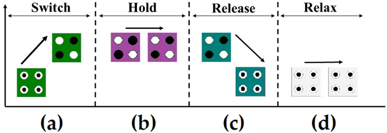
Clocking stands as another crucial aspect of QCA technology, necessitating adherence to specific rules to ensure accurate output generation. Clocking comprises four distinct phases, each imbued with specific significance, as delineated in Fig. 3. The initial phase, known as the switch phase, entails an increase in incoming force on the electrons within the cell, preparing them for fixation. Subsequently, during the hold phase, the incoming force peaks, prompting the cell to adopt a logical value of “0” or “1”. The release phase follows, characterized by a reduction in incoming force, facilitating the transition of electrons from a fixed to a mobile state. Last, but not least, in the fourth phase known as relax phase, the force diminishes to its minimum, enabling electrons to move freely within the cell. In Fig. 3, different clock phases with their colors are shown which (a), (b), (c), and (d) parts are phase 0, phase 1, phase 2, and phase 3, respectively.
| (1) |
| (2) |
| (3) |
Fig. 3.
Clocking in QCA technology, (a) phase 0, (b) phase 1, (c) phase 2, (d) phase 3.
3. Proposed digital code converters
In this part, three new converters by employing tile method are presented. The need for converters that transform BCD to gray, excess-3, and 2421 codes arises from the limitations of BCD and the unique advantages each of these codes offers in various digital applications. While BCD is straightforward for representing decimal numbers, it is less efficient for arithmetic operations, error handling, and state transitions. Gray code ensures that only one-bit changes between successive values, minimizing the risk of errors during state transitions, which is crucial in rotary encoders for robotics, automation, and communication systems to reduce transmission errors. It is also valuable for memory addressing schemes to prevent data corruption. Excess-3 code, a self-complementing code, simplifies subtraction operations without requiring complex circuits, making it highly effective in arithmetic units, such as calculators, digital counters, and ALUs. Additionally, its ability to detect invalid code combinations enhances error detection in communication systems and data storage. Similarly, the 2421 code, being a weighted code, offers faster arithmetic processing with minimal hardware complexity, making it ideal for high-performance ALUs, fault-tolerant (by its self-complementary behavior) computing in automotive and aerospace, and efficient decimal counters and displays. Using these codes instead of BCD improves processing speed, reduces circuit complexity, and enhances reliability. Whilst the first circuit converts a BCD code to its gray code equivalent, the second one gets similar input and converts it to an excess-3 code. The last proposed circuit generates an aiken or 2421 code by getting a BCD code as its input. There is a need for utilizing a XOR gate for both BCD to gray code and BCD to excess-3 code converters so; this gate is designed with tile-based method. The tile-based method in QCA design offers distinct advantages over other techniques, such as gate-based and majority logic-based approaches. Traditional gate-level designs become increasingly complex as circuits grow, whereas the tile-based method enhances modularity by organizing circuits into reusable functional blocks, simplifying the design process. Additionally, it reduces the reliance on intricate wire crossings, lowering signal interference and propagation delays. Unlike error-correction techniques that introduce significant redundancy, the tile-based approach improves fault tolerance by localizing defects within individual tiles, minimizing the impact of faults without excessive overhead. This balance of modularity, fault resilience, and efficiency makes the tile-based method a highly effective strategy for complex QCA circuit design.
BCD is a kind of binary code which is utilized to illustrate a decimal number to its binary equivalent. This number has four bits from 0000 to 1001 standing for 0 to 9. From left to right, each bit's weight is equal to 8, 4, 2 and 1, respectively. Take for example 36.45 to be converted to its BCD equivalent being 0011 0110.0100 0101. In the following, all of the aforementioned converters are detailed.
3.1. The proposed BCD to gray code converter
The gray code, also known as Cyclic Binary Code, is a binary numeral system where each consecutive number differs by only one bit. While both cyclic binary and standard binary systems share the same fundamental digits of 0 and 1 with same weights, 8 4 2 1, they diverge in their representation and utilization. Cyclic binary codes, prioritize error minimization in the representation of measurement units, owing to their sequential numbering schemes. To implement and design the converter generating gray code from the BCD, there is a need for its truth table which can be seen in Table 1. Also, by utilizing the Karnaugh map [21] the relationship between BCD inputs and gray outputs can be achieved. The functions related to G0, G1, G2 and G3 can be seen in equations (4), (5), (6), (7), respectively. The logic circuit of BCD to gray code converter by the mentioned equations is illustrated in Fig. 4.
| (4) |
| (5) |
| (6) |
| (7) |
Table 1.
Truth table of the BCD to gray code converter.
|
BCD Inputs |
Gray Outputs |
||||||
|---|---|---|---|---|---|---|---|
| A | B | C | D | G3 | G2 | G1 | G0 |
| 0 | 0 | 0 | 0 | 0 | 0 | 0 | 0 |
| 0 | 0 | 0 | 1 | 0 | 0 | 0 | 1 |
| 0 | 0 | 1 | 0 | 0 | 0 | 1 | 1 |
| 0 | 0 | 1 | 1 | 0 | 0 | 1 | 0 |
| 0 | 1 | 0 | 0 | 0 | 1 | 1 | 0 |
| 0 | 1 | 0 | 1 | 0 | 1 | 1 | 1 |
| 0 | 1 | 1 | 0 | 0 | 1 | 0 | 1 |
| 0 | 1 | 1 | 1 | 0 | 1 | 0 | 0 |
| 1 | 0 | 0 | 0 | 1 | 1 | 0 | 0 |
| 1 | 0 | 0 | 1 | 1 | 1 | 0 | 1 |
Fig. 4.
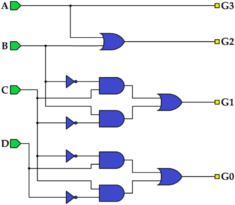
Logic circuit of BCD to gray code converter.
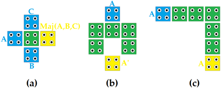
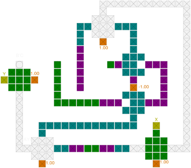
As from Fig. 4 and equations is clear, there is a need for implementing a XOR gate by the tile-based method. To clarify, a majority gate and “NOT gate” by this method can be implemented as Fig. 5 (a) and 5 (b), respectively. Moreover, logical circuit of majority gate can be seen in Fig. 5 (c) while logical circuit of NOT gate is shown in Fig. 5 (d). In Fig. 6(a)–and (b), QCA circuit and logical circuit of an example are presented to depict tile method's mechanism, correspondingly. This circuits gets inputs A and B, and produces AB’ without using a “NOT gate”. This is an advantage of the method resulting in reducing the latency of the circuit. Then the required gates, XOR gate, is shown in Fig. 7. The designed tile-based XOR gate in Fig. 7 (a) has 49 cells and utilizes 3 phases of clock. Also, its logical circuit is illustrated in Fig. 7 (b).
Fig. 5.
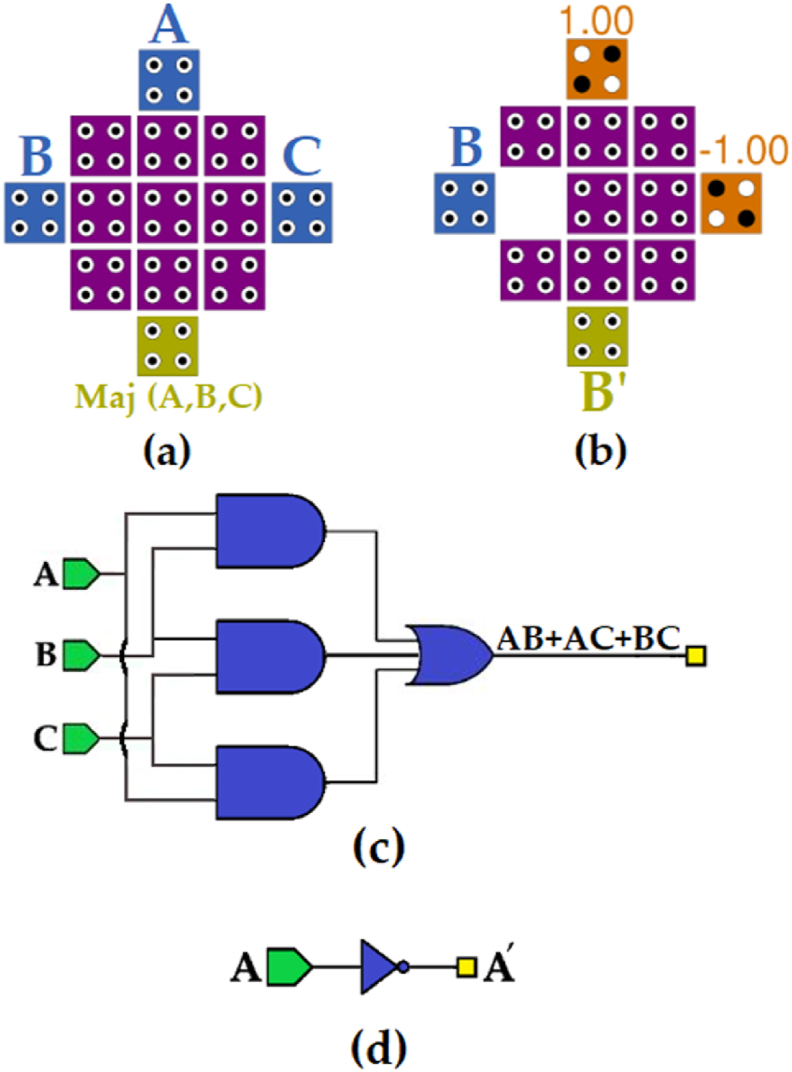
Tile-based method gates, (a) majority gate, (b) NOT gate, (c) logical circuit of majority gate, and (d) logical circuit of NOT gate.
Fig. 6.
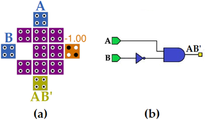
An example to illustrate the mechanism of the tile method, (a) its QCA circuit, and (b) its logical circuit.
Fig. 7.
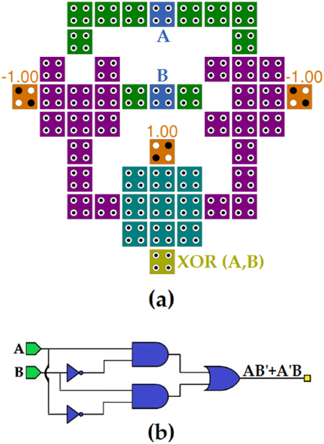
Designing XOR gate (a) by the tile method, and (b) its logical circuit.
To design the proposed BCD to gray code converter, the presented XOR gate (Fig. 7 (a)) is used for implementing both G0 and G1 outputs. For the third output being G3, just a “OR gate” is necessary which can be created by placing a cell with polarization +1 instead of cell “C” in Fig. 5(a). Last, but not least, to generate output G3, just utilizing wire gate is enough. Due to all these considerations, the proposed circuit converting BCD to gray is presented in Fig. 8.
Fig. 8.
The proposed tile-based BCD to gray code converter in QCA.
As it is clear in Fig. 8, there was a need for conveying input C to the left XOR gate. Hence, to do that, a wire crossed over the main layer in the third layer of the proposed circuit. This line is shown in Fig. 9.
Fig. 9.

The crossover line in the proposed BCD to gray code converter.
3.2. The proposed BCD to excess-3 code converter
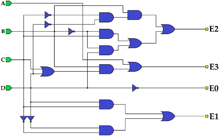
Excess-3 code is another form of binary code. It is useful where decimal numbers need to be represented and manipulated by using binary logic. Its simplicity and compatibility with binary arithmetic make it a useful encoding scheme in digital electronics and communication systems. For the next converter, a BCD to excess-3 code one is investigated and designed. To achieve this converter, the first step is earning its truth table which can be seen in Table 2. On the other hand, Excess-3 code involves adding three units to the input to derive the output. For instance, if the input is 0110, applying excess-3 code would yield 1001. Besides, this converter's logic circuit is presented in Fig. 10 which is obtained by equations (8), (9), (10), (11)).
| (8) |
| (9) |
| (10) |
| (11) |
Table 2.
Truth table of the BCD to excess-3 code converter.
|
BCD Inputs |
Excess-3 Outputs |
||||||
|---|---|---|---|---|---|---|---|
| A | B | C | D | E3 | E2 | E1 | E0 |
| 0 | 0 | 0 | 0 | 0 | 0 | 1 | 1 |
| 0 | 0 | 0 | 1 | 0 | 1 | 0 | 0 |
| 0 | 0 | 1 | 0 | 0 | 1 | 0 | 1 |
| 0 | 0 | 1 | 1 | 0 | 1 | 1 | 0 |
| 0 | 1 | 0 | 0 | 0 | 1 | 1 | 1 |
| 0 | 1 | 0 | 1 | 1 | 0 | 0 | 0 |
| 0 | 1 | 1 | 0 | 1 | 0 | 0 | 1 |
| 0 | 1 | 1 | 1 | 1 | 0 | 1 | 0 |
| 1 | 0 | 0 | 0 | 1 | 0 | 1 | 1 |
| 1 | 0 | 0 | 1 | 1 | 1 | 0 | 0 |
Fig. 10.
Logic circuit of BCD to excess-3 code converter.
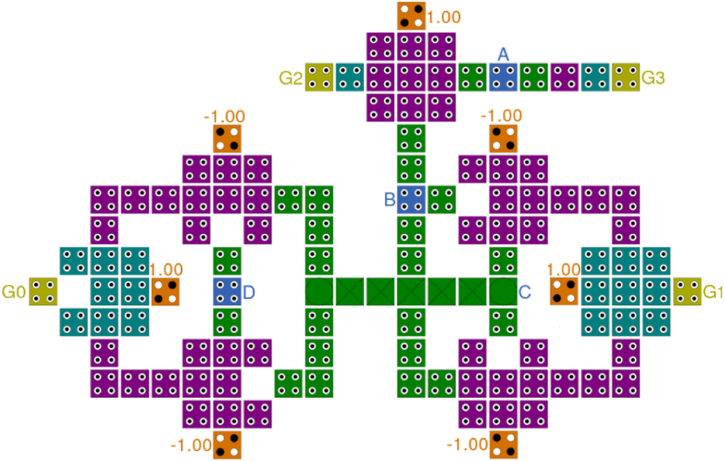
To generate different outputs, various actions are necessary. For the first output, E0, just inverting the input labeled D is enough. In a simple and easy way, E1 is produced by connecting input A to this output's cell via wire. While E2 can be implemented by the XOR gate in Fig. 7 (a), the last output, E3, can be generated by the tile-based XNOR gate in Fig. 11 which its QCA and logical circuit are presented in Fig. 11(a)–and (b), respectively. Eventually, by combining all of these circuits, the proposed circuit converting BCD to excess-3 code can be seen in Fig. 12.
Fig. 11.
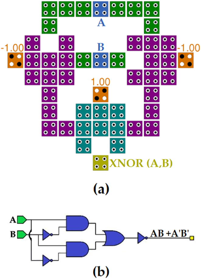
Designing XNOR gate, (a) by the tile method, and (b) its logical circuit.
Fig. 12.
The proposed tile-based BCD to excess-3 code converter in QCA.
3.3. The proposed BCD to aiken (2421) code converter
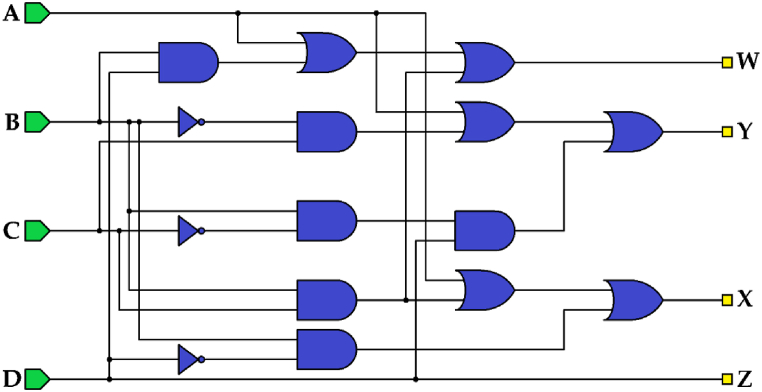
The aiken code is another type of 4-bit binary code where the weights of the bits are assigned in the order of 2, 4, 2, and 1. This code can depict a decimal number just like the BCD code but the difference is that it has a self-complementing behavior. For instance, for decimal number equal to 5, aiken number can be calculated as 1011 or 0101. Based on its characteristic, the former is selected as the correct aiken code for 5. Aiken code offers simplicity, efficiency, and compatibility advantages for applications involving decimal data representation and processing in binary form. Same as other converters, this circuit needs its truth table, which is shown in Table 3, to earn its outputs functions (equation (12), (13), (14), (15))) leading to implementing its logic circuit in Fig. 13.
| (12) |
| (13) |
| (14) |
| (15) |
Table 3.
Truth table of the BCD to aiken code converter.
|
BCD Inputs |
Aiken Outputs |
||||||
|---|---|---|---|---|---|---|---|
| A | B | C | D | W | X | Y | Z |
| 0 | 0 | 0 | 0 | 0 | 0 | 0 | 0 |
| 0 | 0 | 0 | 1 | 0 | 0 | 0 | 1 |
| 0 | 0 | 1 | 0 | 0 | 0 | 1 | 0 |
| 0 | 0 | 1 | 1 | 0 | 0 | 1 | 1 |
| 0 | 1 | 0 | 0 | 0 | 1 | 0 | 0 |
| 0 | 1 | 0 | 1 | 1 | 0 | 1 | 1 |
| 0 | 1 | 1 | 0 | 1 | 1 | 0 | 0 |
| 0 | 1 | 1 | 1 | 1 | 1 | 0 | 1 |
| 1 | 0 | 0 | 0 | 1 | 1 | 1 | 0 |
| 1 | 0 | 0 | 1 | 1 | 1 | 1 | 1 |
Fig. 13.
Logic circuit of BCD to aiken code converter.
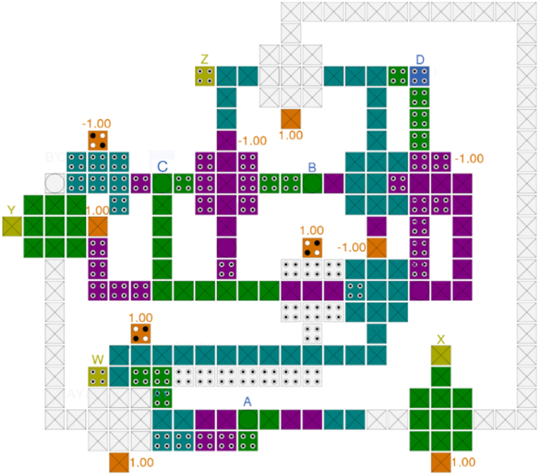
By utilizing equations (12), (13), (14), (15), outputs named Z, Y, X, and W are generated and the proposed tile-based BCD to excess-3 code converter in QCA can be seen in Fig. 14.
Fig. 14.
The proposed tile-based BCD to aiken code converter in QCA.
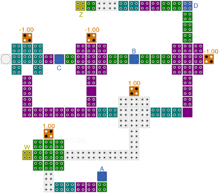
The presented circuit consists of three layers. The first one, as Main layer, contains the main part of the designed converter illustrated in Fig. 15. Also, while Fig. 16 shows the Via layer with just 6 cells, the last layer, Top layer, is another big layer which contains a considerable number of cells. This layer is presented in Fig. 17.
Fig. 15.
Main layer of the proposed tile-based BCD to aiken code converter in QCA.
Fig. 16.
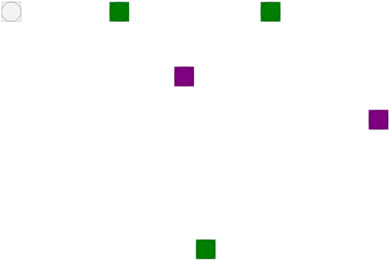
Via layer of the proposed tile-based BCD to aiken code converter in QCA.
Fig. 17.
Top layer of the proposed tile-based BCD to aiken code converter in QCA.
4. Simulation and results
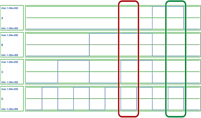
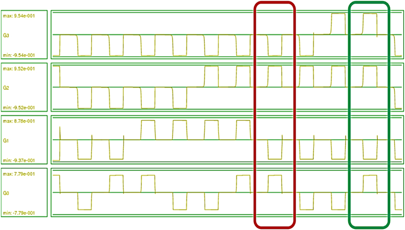
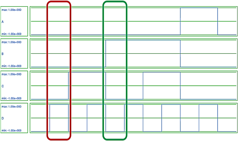
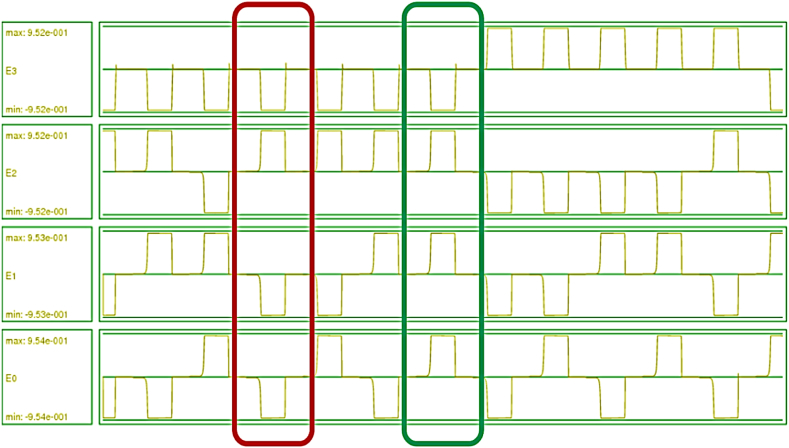
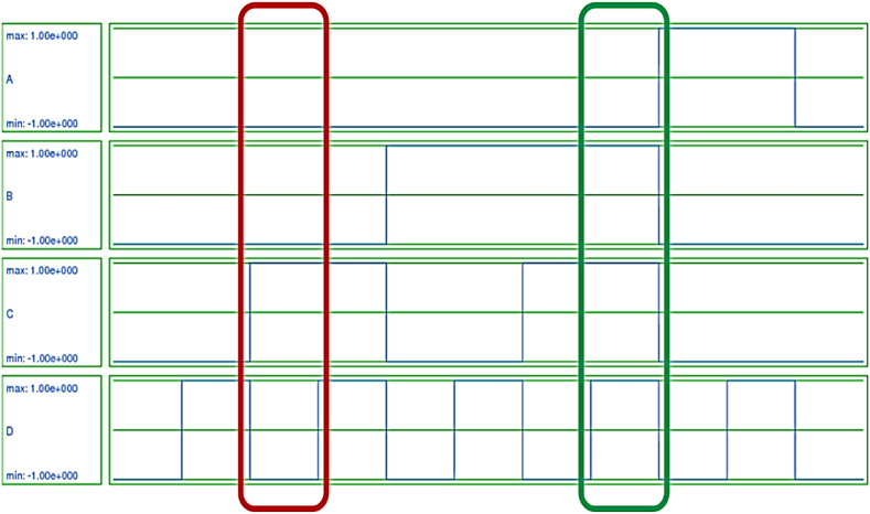
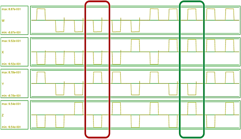
In this part, the QCADesigner-E version 2.2, as a widely-used software in this field, is utilized. Since QCA is still in the early stages of development, and there are limitations in QCA fabrication technology, and physical prototyping is not widely feasible yet, simulation tools are currently the primary and most accepted approach for validating QCA-based designs. Hence, in this study, QCADesigner-E is utilized for validating circuits' outcome. Aside from investigating in the correctness of the proposed circuits, this software reports some important factors such as cell count, power consumption, occupied are, etc. [22,23]. To simulate and run circuits, the “Bistable Approximation” is selected as the “Simulation Engine Setup”. To investigate circuits much more precise, “Number of Samples” is set to 100000. While the “Radius of Effect” parameter is considered 45 nm, the “Convergence Tolerance” is equal to 0.0001, ten times lower than its default value. Also, the “Maximum Iterations per Sample” is considered 1000. For other parameters such as “Relative Permittivity”, “Clock High”, “Clock Low”, “Clock Shift”, “Clock Amplitude Factor”, and “Layer Separation”, the default values are considered being equal to 9.8e-022, 3.8e-023, 0.0e+000, 2.0, and 11.5, respectively. As it was detailed in previous section, there are three converters which were presented in this study. The first circuit, BCD to gray code converter's inputs and outputs are illustrated in Fig. 18, Fig. 19, respectively. As it is clear, inputs are from 0000 to 1001 standing from 0 to 9 in decimal. Similarly, for the proposed BCD to excess-3 code converter, as the second presented circuit, Fig. 20 shows inputs for it and excess-3 code as this circuit's output is shown in Fig. 21. Finally, while Fig. 22 depicts BCD inputs for the third proposed converter, Fig. 23 presents its outcome which is supposed to be aiken code equivalent of BCD inputs.
Fig. 18.
BCD inputs of the first proposed circuit to generate gray code.
Fig. 19.
Generated gray code by the first proposed circuit getting BCD input.
Fig. 20.
BCD inputs of the second proposed circuit to generate excess-3 code.
Fig. 21.
Generated excess-3 code by the second proposed circuit getting BCD input.
Fig. 22.
BCD inputs of the third proposed circuit to generate aiken code.
Fig. 23.
Generated aiken code by the third proposed circuit getting BCD input.
In the following to evaluate the proposed circuits, some examples are investigated and presented. When there is a BCD equal to 0110, G3, G2, G1 and G0 has to be equal to binary “0”, “1”, “0” and “1”, respectively. In a similar way, by applying a BCD number equal to 1001 to a BCD to gray code converter, its output must be 1101. By looking at outcomes generating by the BCD to gray code converter, it can be realized that this circuit does the conversion in a completely correct way. 127 cells were used to implement this converter occupying an area equal to 0.18 μm2. Moreover, this circuit generated required gray code outputs by employing 3 phases of clock along with 55.3 meV of total power consumption. To convert a BCD code to excess-3 code by the proposed BCD to excess-3 code converter, by applying a BCD code equal to 0001, the generated excess-3 code must be 0001 + 0011 being 0100. Besides, when the input of this converter is a BCD code equal to 0100, the produced excess-3 code must be equal to 0111. By checking the proposed converter's outcomes, its results in generating excess-3 code from BCD code by consuming power equal to 53.7 meV and 7 phases of clock along with utilizing 190 cells in and area equal to 0.25 μm2 is completely valid. Eventually, the proposed BCD to aiken code have to keep the self-complementary behavior of the nature of the aiken code. So, by giving a BCD code equal to 0010 and 0111, the generated aiken code must be equal to 0010 and 1101. By taking a look at these outcomes, the self-complementary of them can be seen. Hence, the performance of this circuit is completely correct. To design and simulate this converter, 287 cells in an area equal to 0.22 μm2 were used. Plus, it employed 5 clocking phases with the power consumption of 102 meV.
To compare the presented converters, 10 similar previous circuits were selected and then compared in Table 4 in terms of type of conversion, cell number, occupied area (total area), latency, the ability of salability, the number of used inverter gate, and the type of layering. One of the most important key factors in increasing the latency of circuits is “NOT gate” decreasing the usage of this gate is one of the most prominent merits of the proposed converters. While the BCD to excess-3 code used only 3 inverter gates, there was nothing about utilizing this gate to do with the proposed BCD to gray code and BCD to aiken code converters. This happened when all references used this gate in their presented circuits from 3 to 19 gates. Moreover, due to using tile method in designing the proposed converters, they are the only converters with that ability of scalability making manufacturers enable to integrate their circuits. This is another important advantage of the proposed converters. In terms of cells number and occupied area, the three proposed converters are better than all of other circuits. Finally, about the last factor being latency, the proposed BCD to gray code, BCD to aiken code and BCD to excess-3 code converters had a latency equal to 0.75, 1.25 and 1.75. All in all, the proposed converters showed a very good level of accuracy and speed along with a minimal size and power usage.
Table 4.
Comparing all three proposed converters with some similar circuits.
| Circuit | Type of conversion | Cell number | Occupied area (μm2) | Latency | Scalability | Inverter gate number | Type of layering |
|---|---|---|---|---|---|---|---|
| [14] | Binary to gray | 137 | 0.16 | 0.5 | No | 6 | Single-layer |
| [15] | Binary to gray | 217 | – | – | No | 9 | Single-layer |
| [24] | Binary to gray | 225 | 0.43 | 1.00 | No | 3 | Multilayer |
| [25] | Thermometer code to gray | 134 | 0.20 | 1.75 | No | 7 | Single-layer |
| [26] | Binary to gray | 389 | 0.69 | 8.00 | No | – | Single-layer |
| [26] | Binary to excess-3 | 413 | 0.63 | 8.00 | No | – | Single-layer |
| [27] | BCD to excess-3 | 414 | 0.52 | 2.25 | No | 19 | Multilayer |
| [28] | BCD to excess-3 | 191 | 0.29 | 3.00 | No | 4 | Single-layer |
| [29] | BCD to excess-3 | 254 | 0.31 | 1.00 | No | 4 | Multilayer |
| First | BCD to gray | 127 | 0.18 | 0.75 | Yes | 0 | Multilayer |
| Proposed circuit | |||||||
| Second | BCD to excess-3 | 190 | 0.25 | 1.75 | Yes | 3 | Single-layer |
| Proposed circuit | |||||||
| Third | BCD to aiken | 287 | 0.22 | 1.25 | Yes | 0 | Multilayer |
| Proposed circuit |
It is to be noted that, the tile-based approach is highly effective in addressing key challenges in QCA circuit design, particularly interconnections and wire crossings. By organizing the circuit into localized tiles, the design minimizes the need for extensive interconnections, ensuring faster and more efficient signal transmission. Wire crossings, a common source of noise and signal interference in QCA, are also significantly reduced in tile-based layouts, as most signal interactions occur within individual tiles rather than across the entire circuit. Employing the tile-based method in the design and optimization of the proposed converters not only simplified the layout but also enhanced the reliability and integrity of signal propagation. Furthermore, to minimize the number of cells, used area, clock phases, and circuit complexity, precise configurations of the majority and inverter gates, including their placement strategies and functional roles within the tile-based design, were thoroughly investigated. Ultimately, the most optimized code converters were achieved by employing the tile-based method in QCA technology.
5. Conclusion
This study introduced three novel code converters, the BCD to gray, BCD to excess-3, and BCD to aiken (2421), using the tile-based approach in Quantum-dot Cellular Automata technology. The tile-based method facilitated the integration of majority and inverter gates within the same structure, addressing challenges in conventional designs that often lead to increased circuit size and latency. The proposed converters demonstrated significant optimizations, including reductions in cell count, occupied area, and power consumption. Specifically, the BCD to gray converter achieved a 7.3 % reduction in the number of cells and eliminated the need for NOT gates entirely. The BCD to excess-3 converter reduced the required cells by 0.5 %, area by 13.8 %, clock phases by 41.7 %, and NOT gates by 25 % compared to existing designs. These results underscore the potential of the tile-based QCA approach for developing compact, efficient, and low-power digital systems. However, some limitations of the current study should be noted. The converters were evaluated based on specific design parameters, such as the number of clock phases and NOT gates, leaving room to explore other aspects like fault tolerance and thermal stability. Future research could focus on these areas and assess the converters' performance under different environmental conditions. Furthermore, the tile-based approach holds promise for broader applications beyond code converters. Future work could explore its use in more complex digital circuits, such as arithmetic units or memory elements, to further capitalize on its scalability and optimization potential.
CRediT authorship contribution statement
Farhad Fouladinia: Writing – review & editing, Writing – original draft, Validation, Software, Resources, Methodology, Investigation, Formal analysis. Mohammad Gholami: Writing – review & editing, Visualization, Validation, Supervision, Software, Project administration, Methodology, Investigation, Conceptualization. Pardis Karimi: Writing – review & editing, Software, Methodology, Investigation.
Data and code availability
Data and code will be made available on request.
Declaration of competing interest
The authors declare that they have no known competing financial interests or personal relationships that could have appeared to influence the work reported in this paper.
References
- 1.Gholami M., Movahedi M., Amirzadeh Z. Latch and flip-flop design in QCA technology with a minimum number of cells. Comput. Electr. Eng. 2022;102 [Google Scholar]
- 2.Lent C.S., Tougaw P.D., Bernstein G.H. Quantum cellular automata. Nanotechnology. 1993;4(1):49. [Google Scholar]
- 3.Zoka S., Gholami M. A novel efficient full adder–subtractor in QCA nanotechnology. Int. Nano Lett. 2019;9(1):51–54. [Google Scholar]
- 4.Gholami M., Khakpour M., Naghizadeh S. Parity generator and digital code converter in QCA nanotechnology. Int. Nano Lett. 2020;10(1):49–59. [Google Scholar]
- 5.Huang J., Momenzadeh M., Schiano L., Ottavi M., Lombardi F. Tile-based QCA design using majority-like logic primitives. ACM J. Emerg. Technol. Comput. Syst. 2005 Oct 1;1(3):163–185. [Google Scholar]
- 6.Fouladinia F., Gholami M. Decimal to excess-3 and excess-3 to decimal code converters in QCA nanotechnology. Int. J. Eng. 2023 Sep 1;36(9):1618–1625. [Google Scholar]
- 7.Raina H., Verma C.H., Gupta M., Sharma V.K. 5th International Conference on Trends in Electronics and Informatics (ICOEI) 2021. Binary coded decimal (BCD) seven segment circuit designing using quantum-dot cellular automata (QCA) [Google Scholar]
- 8.Kaity A., Singh S. Optimized area efficient quantum dot cellular automata based reversible code converter circuits: design and energy performance estimation. J. Supercomput. 2021;77:11160–11186. [Google Scholar]
- 9.Mukherjee C., Panda S., Mukhopadhyay A.K., et al. Towards modular binary to gray converter design using LTEx module of quantum-dot cellular automata. Microsyst. Technol. 2019;25:2011–2018. [Google Scholar]
- 10.Fouladinia F., Gholami M. Decimal to excess-3, BCD, and gray code converters with a novel 4-inputs block in QCA. Opt. Quant. Electron. 2023 Oct;55(10):862. [Google Scholar]
- 11.You Y., Jeon J. Design of extendable BCD-EXCESS-3 code convertor using quantum-dot cellular automata. The Journal of Advanced Navigation Technology. 2016;20(1):65–71. [Google Scholar]
- 12.Misra N.K., Sen B., Wairya S., Bhoi B. InProceedings of the Second International Conference on Computational Intelligence and Informatics: ICCII 2017. Springer Singapore; Singapore: 2018 Jul 24. A novel parity preserving reversible binary-to-BCD code converter with testability of building blocks in quantum circuit; pp. 383–393. [Google Scholar]
- 13.Fouladinia F., Gholami M. Design of a novel decimal to multicode converter in QCA technology. Journal of Electrical and Computer Engineering. 2023 Oct 7:2023. [Google Scholar]
- 14.Ahmad F., Bhat G. Novel code converters based on quantum-dot cellular automata (QCA) Int. J. Sci. Res. 2014 May;3(5):364–371. [Google Scholar]
- 15.Ilanchezhian P., Parvathi R.M. Nanotechnology based effective design approach for code converter circuits using QCA. International Journal of Computer Applications. 2013 Jan 1;69(8) [Google Scholar]
- 16.Seyedi S., Navimipour N.J. A fault-tolerance nanoscale design for binary-to-gray converter based on QCA. IETE J. Res. 2023 Jul 4;69(5):2991–2998. [Google Scholar]
- 17.Gassoumi I., Touil L., Ouni B. Design and Testing of Reversible Logic. 2020. Design of reversible binary-to-gray code converter in quantum-Dot cellular automata; pp. 251–261. [Google Scholar]
- 18.Safaiezadeh B., Kettunen L., Haghparast M. Novel high-performance QCA Fredkin gate and designing scalable QCA binary to gray and vice versa. J. Supercomput. 2023 Apr;79(6):7037–7060. [Google Scholar]
- 19.Galadima BY, Galadanci GS. QCA-BASED design of reversible hamming code encoding, Decoding and Correcting Circuits.
- 20.Xie C., Zhao X., Navimipour N.J. Design and analysis of a fault tolerance nano-scale code converter based on quantum-dots. Nano Communication Networks. 2024 Dec 1;42 [Google Scholar]
- 21.Karnaugh M. The map method for synthesis of combinational logic circuits. Transactions of the American Institute of Electrical Engineers, Part I: Communication and Electronics. 1953 Nov;72(5):593–599. [Google Scholar]
- 22.Sill Torres F., Willie R., Niemann P., Drechsler R. An energy-aware model for the logic synthesis of quantum-dot cellular automata. IEEE Trans. Comput. Aided Des. Integrated Circ. Syst. 2018;37(12):3031–3041. [Google Scholar]
- 23.Walus K., Dysart T.J., Jullien G.A., Budiman R.A. QCADesigner: a rapid design and Simulation tool for quantum-dot cellular automata. IEEE Trans. Nanotechnol. 2004;3:26–31. [Google Scholar]
- 24.Guleria N. In2017 3rd International Conference on Advances in Computing, Communication & Automation (ICACCA)(Fall) IEEE; 2017 Sep 15. Binary to gray code converter implementation using QCA; pp. 1–6. [Google Scholar]
- 25.Das J.C., De D. Design of thermometer code-to-gray code converter circuit in quantum-dot cellular automata for nano-computing network. Photonic Netw. Commun. 2021 Jun;41(3):259–273. [Google Scholar]
- 26.Iqbal J., Khanday F.A., Shah N.A. Efficient quantum dot cellular automata (QCA) implementation of code converters. Communications in Information Science and Management Engineering. Oct. 2013;3(10):504–515. [Google Scholar]
- 27.You Y., Jeon J. Design of extendable bcd-excess 3 code convertor using quantum-dot cellular automata. J Adv Navigation Technol. 2016;20(1):65–71. doi: 10.12673/jant.2016.20.1.65. [DOI] [Google Scholar]
- 28.You Y., Jeon J. Efficient design of bcd-excess 3 code converter using quantum-dot cellular automata. J Adv Navigation Technol. 2013;17(6):700–704. doi: 10.12673/jkoni.2013.17.6.700. [DOI] [Google Scholar]
- 29.Rahman A., Habib A., Bahar A.N., Rahman Z. Novel design of BCD to Excess-3 code converter in quantum dots cellular automata (QCA) Global J Research Eng. 2014;14(4):8–11. [Google Scholar]
Associated Data
This section collects any data citations, data availability statements, or supplementary materials included in this article.
Data Availability Statement
Data and code will be made available on request.


