Abstract
In this work, CsPb.625Zn.375IBr2-based perovskite solar cells (PSCs) are numerically simulated and optimized under ideal lighting conditions using the SCAPS-1D simulator. We investigate how various hole transport layers (HTL) including Zn3P2, PTAA, MoS2, MoO3, MEH-PPV, GaAs, CuAlO2, Cu2Te, ZnTe, MoTe2, CMTS, CNTS, CZTS, CZTSe and electron transport layers (ETL) such as CdS, SnS2, ZnSe, PC60BM interact with the devices’ functionality. Following HTL material optimization, a maximum power conversion efficiency (PCE) of 16.59% was observed for the FTO/SnS2/CsPb.625Zn.375IBr2/MoS2/Au structure, with MoS2 proving to be a more economical option. The remainder of the investigation is done following the HTL optimization. We study how the performance of the PSC is affected by varying the materials of the ETL and to improve the PCE of the device, we finally optimized the thickness, charge carrier densities, and defect densities of the absorber, ETL, and HTL. In the end, the optimized arrangement produced a VOC of 0.583 V, a JSC of 43.95 mA/cm2, an FF of 82.17%, and a PCE of 21.05% for the FTO/ZnSe/CsPb.625Zn.375IBr2/MoS2/Au structure. We also examine the effects of temperature, shunt resistance, series resistance, generation rate, recombination rate, current-voltage (JV) curve, and quantum efficiency (QE) properties to learn more about the performance of the optimized device. At 300 K, the optimized device provides the highest thermal stability. Our research shows the promise of CsPb.625Zn.375IBr2-based PSCs and offers insightful information for further development and improvement.
Keywords: Double perovskite solar cell, CsPb.625Zn.375IBr2 light absorber, ZnSe ETL, MoS2 HTL, SCAPS-1D
Subject terms: Materials science, Physics
Introduction
Perovskite solar cells (PSCs) are regarded as one of the more viable variants for harnessing solar energy due to their appealing bandgap, high carrier mobility, and high absorption coefficient, among other desired optoelectronic attributes1–4. PSCs present a cost-effective and straightforward deposition method for harvesting solar energy compared to silicon solar cells5–8. Moreover, the power conversion efficiency (PCE) of PSCs has risen dramatically throughout the preceding 12 years, rising from 3.8 to 26.1%, enabling them to contend with silicon solar cells9–11.
The perovskite material has the chemical formula ABX3, where A represents an organic cation [CH3NH3+], B represents a divalent metal ion (Pb2−, Sn2−), and X (Br−, I−, Cl−) represents a halide ion when positioned at the body middle of the octahedron, six halide anions surround cation B, which has favorable bandgaps, high absorption coefficient, lingering carrier diffusion length, exalted carrier mobility, and superb carrier lifetime12,13. However, despite exhibiting excellent optoelectronic properties and evolutionary success in PCE within a very short time, the lack of lingering-term stability is still taken into account as the biggest hindrance to making PSCs commercially available14. Under the influence of UV light, redox reactions trigger chemical decomposition. Moreover, the polarity of water molecules adversely affects the hydrogen bonds of perovskites15,16. As a result, the stability of PSCs decreases when they are exposed to moisture, UV light, and the surrounding environment. This leads to an inevitable deterioration in PSC performance within a few weeks15–17. Therefore, improving the stability of perovskite has taken special attention in recent years so that stable PSCs can be achieved without compromising performance.
Different strategies are investigated to address these issues and improve perovskite stability. Two-dimensional (2D) perovskite and inorganic perovskite are possible solutions to the stability issues18–20. However, 2D perovskite is not an ideal option for developing high-performance PSCs due to its huge bandgaps, asymmetric crystallographic orientations, as well as lengthy organic cation layers, which limit high carrier generation and slow effective charge carrier separation12,21. So, inorganic perovskite materials can be used in solar cells to improve the PSC’s steadiness and retain their efficiency22,23. Cesium ions (Cs+) can be used as a replacement for organic cations to enhance the resilience of materials composed of perovskites20. In 2012, Cs-based CsSnI3 perovskite was introduced, achieving an efficiency of 0.88%24. Since then, many cesium lead halide perovskites have been formed to be utilized in perovskite solar cells (PSCs), including CsPbI3, CsPbBr3, and CsPbCl325–29. CsPbI3 has demonstrated a maximum PCE of ∼19% as of 202130. The PCE of CsPbX3-based devices is still lower than that of their organic-inorganic counterparts, even with the notable advancements in this area. So, to take into account the benefits of inorganic perovskites’ inherent photostability and ensure the achievement of high efficiency of a single-cell structure and cutting-edge approaches like replacing the materials.
PSCs comprised of a CsPb.625Zn.375IBr2 absorber layer are promising because of their opt electrical properties31,32. Based on our knowledge, CsPb0,625Zn0.375IBr2 absorber material has not yet been explored experimentally. However, similar halide perovskites, such as CsSnxGe1−xIyBr3 − y, CsPbxSn1−xIyBr3 − y have been successfully synthesized and studied in experimental setups33–35. Prior studies have identified several significant challenges during fabrication, including maintaining stability, preventing defects, achieving homogeneous morphology, and controlling stoichiometry36. According to those investigations, maximizing the characteristics and device performance of these above-mentioned perovskites requires controlling morphological defects, such as surfaces or heterointerfaces, intragrain defects, and grain boundaries37,38. Achieving a high-quality perovskite thin film with characteristics such as dense, uniform, pinhole-free layers, large grain sizes, and low grain boundary density has proven beneficial for device performance. Common fabrication methods such as one-step spin-coating and two-step deposition also have been employed to synthesize these perovskite thin films for achieving high-quality uniform layers. To enhance stability especially additive engineering has been applied in similar perovskite films, which may also be applicable to CsPb0,625Zn0.375IBr239,40.
In addition, the determination of adequate ETL and HTL amalgamation can significantly contribute towards increasing the PCE of these emerging devices41–43. Moreover, the thicknesses of the ETL HTL, along with their interface and phase-matching properties, profoundly impact solar metrics including PCE, fill factor (FF), short-circuit current density (JSC), and open-circuit voltage (VOC)41–45.
Specifically, the ETL is an indispensable aspect of a PSC because it extracts electrons from the perovskite absorber and inhibits holes in it. To further boost the PCE of PSC, the scientific community has been meticulously tracking the introduction of new materials through the previously indicated pathway, especially in ETL. TiO2, ZnO, and SnO2 are examined extensively for PSCs46–49. New ETLs are still one of the major concerns in the research community. Recently, Liu et al. achieved 11.2% efficiency with all-low-temperature processed PSCs using CdS as ETL. Peng et al. reported an even higher efficiency of 15%50. Tin Sulfide (SnS2) is a cost-effective metal sulfide with unique chemical and structural properties, making tunable bandgap ideal for PSC51. After studying Mg-doped ZnO (MZO) and the impact of Mg concentration on their optical characteristics and structure, it was determined that Mg-doped ZnO films could be appropriate for PSCs52. Zinc Selenide (ZnSe) has been devoted as an ETL in PSCs due to its excellent electron mobility and 2.8 eV straight bandgap. It might function as an n-type collecting layer for reliable and productive commercial PSCs53. PSCs with as-deposited [6, 6]-phenyl-C60-butyric acid methyl ester (PC60BM) layer displayed no photocurrent hysteresis, even without thermal treatment54. So, in comparative analysis, these five ETLs performed superbly in PSCs.
Conversely, though, the HTL impacts solar device manufacturing costs, stability, and efficacy. Materials that are both organic and inorganic are utilized to find the more efficient, stable, and low-cost HTLs55–57. However, recent research shows that the superior band alignment, affordability, and stability of inorganic and small molecule HTLs contribute to improved solar cell performance58–63. Different organic and inorganic HTLs, Zinc Phosphide (Zn3P2), Poly[bis(4-phenyl)(2,4,6-trimethylphenyl)amine (PTAA), Molybdenum disulfide (MoS2), Molybdenum trioxide (MoO3), Poly[2-methoxy-5-(2’-ethylhexyloxy)-1,4-phenylene vinylene] (MEH-PPV), Gallium arsenide (GaAs), Copper aluminum oxide (CuAlO2), Copper Telluride (Cu2Te), Zinc Telluride (ZnTe), Molybdenum Telluride (MoTe2), Copper zinc tin sulfide (CZTS), copper zinc tin selenide (CZTSe), copper manganese tin sulfide (CMTS), and copper-nickel tin sulfide (CNTS) will be analyzed in PSCs because of its tunable band gap.
In this work, we outline the layout and execution of a CsPb.625Zn.375IBr2 -based perovskite-based solar cell using a unique device architecture: FTO/ETL/CsPb.625Zn.375IBr2/HTL/Au. This work considers HTLs Zn3P2, PTAA, MoS2, MoO3, MEH-PPV, GaAs, CuAlO2, Cu2Te, ZnTe, MoTe2, CMTS, CNTS, CZTS, CZTSe as HTLs, CdS, SnS2, ZnSe, PC60BM as ETLs. To leverage optimal cell output, we offer detailed investigations of the effects of the degree of doping and ETL/HTL layer thickness, perovskite interface layers, electron/hole transport layer separation, absorber layer thickness, and perovskite defect density on PV parameters using the SCAPS-1D in this work64. Furthermore, the ramifications of recombination rates, J-V, QE, operating temperature, and series and shunt resistance were assessed in PV performance generation. Finally, a comparison with earlier research was done using the discovered solar cell characteristics. These results imply that our method of device optimization offers a special set of abilities to PSC research that may be used in a real-world device fabrication process in the lab, saving the researchers money and time.
Device modeling and device structure
Device modeling
SCAPS-1D has been employed to simulate the device characteristics of perovskite-based solar cells. With SCAPS-1D, a strong correlation between simulation and experimental data could be demonstrated65. The SCAPS-1D software for simulating optoelectronic devices was developed by the Department of Electronics and Information Systems (ELIS) at the University of Gent64. SCAPS is frequently employed in simulations of optoelectronic devices, notably for solar energy device research since it is capable of resolving the Poisson equations. (Eq. 1) and continuity equations (Eqs. 2–3) to estimate PV device output64.
 |
1 |
 |
2 |
 |
3 |
Where Jn and Jp are considered electron and hole concentrations respectively. Which are described in (Eqs. 4–5).
 |
4 |
 |
5 |
SCAPS may accept seven distinct material layers and front and back contact layers. Furthermore, SCAPS contextualizes and provides an impeccable venue for this research due to its user-friendly options, which include various defect energy distributions (Gauss, Uniform, tail, single level, or combination), intricate defect shapes (interface or bulk defect), and defect charge types (idealization, monovalent, divalent, and multivalent)64. Photovoltaic characteristics (efficiency, JSC, FF, and VOC) with defect density (Eqs. 6–10) to forecast PSCs characteristics2.
 |
6 |
 |
7 |
 |
8 |
 |
9 |
 |
10 |
This study focuses on device optimization based on the PV parameters of solar cell devices. SCAPS-1D is a powerful simulator that can model the electrical characteristics of solar cells66–69, including current-voltage (I-V) curves, capacitance-voltage (C-V) relationships, capacitance-frequency (C-f) responses, quantum efficiency profiles, and so on. Such electrical modeling plays a crucial role in determining solar cell device performance, enabling the optimization of parameters like layer thickness, doping density, and defect density. However, it is important to acknowledge that optical simulations also play a critical role in optimizing the design of solar cells as supported by previous studies70,71. Optical modeling not only enables more accurate calculations of layer thicknesses but also provides valuable insights into material selection for enhancing light absorption and minimizing reflection. Three macroscopic parameters including photon absorption, the energy band gap of the material, and device resistance—are crucial for determining power-conversion efficiency72–75. Additionally, in thin-film solar cells, optical interference effects significantly influence light absorption, underscoring the necessity of optical modeling for improving absorption efficiency. However, optical modeling was omitted in this study as our primary objective was to establish a solid understanding of the device’s electrical characteristics.
Device structure
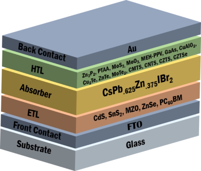
An n-i-p planar heterojunction structure consisting of the ETL, HTL CsPb.625Zn.375IBr2 absorber, transparent Fluorine doped tin oxide (FTO), and gold (Au) back contact was simulated on SCAPS-1D for this investigation, as shown in Fig. 1. In every device structure, the absorber layer CsPb.625Zn.375IBr2 lies in the space between the HTL and the ETL. The p-region is represented by the HTL, the i-region by the CsPb.625Zn.375IBr2 absorber, and the n-region by the ETL. When exposed to light, the absorber layer of the solar cell forms electron-hole pairs, with the electrons and holes moving in the directions of the n- and p-layers, respectively. Electrons and holes can migrate and separate because of the electrical field that exists beneath the two layers.
Fig. 1.
PSC structure based on CsPb.625Zn.375IBr2 absorber.
The study examines the efficacy and efficiency of ten HTL and four ETL-based optimized PSC structures. As used in the SCAPS-1D simulation in this work, Tables 1 and 2 displays the optoelectronic properties of the FTO, ETLs (CdS, SnS2, ZnSe, PC60BM), absorber layer (CsPb.625Zn.375IBr2), and HTLs (Zn3P2, PTAA, MoS2, MoO3, MEH-PPV, GaAs, CuAlO2, Cu2Te, ZnTe, MoTe2, CMTS, CNTS, CZTS, CZTSe). With 4.4 eV of work function, an FTO is utilized and the thickness of FTO is assumed to be 200 nm. Device performance is optimized by varying the thickness of the absorber, HTL, and ETL layers across a wide range. The temperature at which the simulation runs is 300 K under a single sun’s radiation (100 mW/cm2, AM1.5G).
Table 1.
Input parameters of the FTO, absorber, and ETL in this study.
| Material property | FTO | SnS2 | ZnSe | CdS | PC60BM | CsPb0.625Zn0.375IBr2 (absorber) |
|---|---|---|---|---|---|---|
| Thickness (nm) | 200 | 150 | 70 | 50 | 50 | 50–500 nm |
| Bandgap, Eg (eV) | 3.5 | 1.85 | 2.81 | 2.4 | 1.8 | 1.05 |
| Electron affinity, Χ (eV) | 4.00 | 4.26 | 4.09 | 4.18 | 4.2 | 4.27 |
| Relative dielectric permittivity, εr | 9.00 | 17.7 | 8.6 | 10 | 4 | 6 |
| Conduction band effective density of states NC (1/cm3) | 2.2 1018 1018
|
7.32 1018 1018
|
2.2 1018 1018
|
2.2 1018 1018
|
1 1021 1021
|
1 × 10¹⁹ |
| Valence band effective density of states NV (1/cm3) | 1.8 1019 1019
|
1 1019 1019
|
1.8 1018 1018
|
1 1019 1019
|
 1020 1020
|
1 × 10¹⁹ |
| Electron thermal velocity (cm s− 1) | 107 | 107 | 107 | 107 | 107 | 107 |
| Hole thermal velocity (cm s− 1) | 107 | 107 | 107 | 107 | 107 | 107 |
| Electron mobility, µn (cm2/Vs) | 20 | 50 | 4 102 102
|
100 | 0.1 | 25 |
| Hole mobility, µh (cm2/Vs) | 10 | 25 | 1.1 102 102
|
25 | 0.1 | 25 |
| Donor density, ND (1/cm3) | 1018 | 9.85 1019 1019
|
1 1018 1018
|
1 1018 1018
|
1 1017 1017
|
1 × 10¹⁵ |
| Acceptor density, NA (1/cm3) | 0 | 0 | 0 | 0 | 0 | 1 × 10¹⁵ |
| Total density (cm− 3) | 1015 | 1014 | 1 1015 1015
|
1 1015 1015
|
1 1015 1015
|
1 × 10¹² |
| Reference | 76 | 77 | 76 | 78 | 79 | 32 |
Table 2.
Input parameters of HTL in this study.
| Material property | PTAA | GaAs | ZnTe | CNTS | MoO3 | MEH-PPV | CuAlO2 | MoS2 | Cu2Te | Zn3P2 |
|---|---|---|---|---|---|---|---|---|---|---|
| Thickness (nm) | 150 | 150 | 250 | 100 | 100 | 50 | 350 | 200 | 250 | 250 |
| Bandgap, Eg (eV) | 2.96 | 1.42 | 2.25 | 1.74 | 3.0 | 2.1 | 3.46 | 1.29 | 1.18 | 1.5 |
| Electron affinity, Χ (eV) | 2.3 | 4.07 | 3.73 | 3.87 | 2.3 | 2.8 | 2.5 | 4.2 | 4.2 | 4.2 |
| Relative dielectric permittivity, εr | 9 | 12.9 | 7.3 | 9 | 18 | 3 | 60 | 3 | 10 | 7.11 |
| Conduction band effective density of states NC (1/cm3) | 2.0 × 10²¹ | 2.2 × 10¹⁸ | 2.2 1018 1018
|
2.2 1018 1018
|
1 1019 1019
|
2.5 1019 1019
|
2.2 1018 1018
|
2.2 1018 1018
|
7.8 1017 1017
|
2.2 1018 1018
|
| Valence band effective density of states NV (1/cm3) | 2.0 × 10²¹ | 1.8 1019 1019
|
1.8 1019 1019
|
1.8 1019 1019
|
2.2 1018 1018
|
2.5 1019 1019
|
1.8 1019 1019
|
1.9 1019 1019
|
1.6 1019 1019
|
1.8 1019 1019
|
| Electron thermal velocity (cm s− 1) | 107 | 107 | 107 | 107 | 107 | 107 | 107 | 107 | 107 | 107 |
| Hole thermal velocity (cm s− 1) | 107 | 107 | 107 | 107 | 107 | 107 | 107 | 107 | 107 | 107 |
| Electron mobility, µn (cm2/Vs) | 1 | 8500 | 300 | 11 | 210 | 0.5 10−4 10−4
|
2 | 100 | 500 | 1 |
| Hole mobility, µh (cm2/Vs) | 40 | 400 | 100 | 11 | 210 | 0.5 10−5 10−5
|
8.6 | 150 | 100 | 10 |
| Donor density, ND (1/cm3) | 0 | 0 | 0 | 0 | 0 | 0 | 0 | 0 | ||
| Acceptor density, NA (1/cm3) | 1 1018 1018
|
1 1011 1011
|
1.0 1016 1016
|
1.0 1019 1019
|
1 1018 1018
|
1 1015 1015
|
3 1018 1018
|
1 1017 1017
|
1.0 1021 1021
|
1.0 1019 1019
|
| Total density (cm− 3) |
Acceptor 1 |
1 1014 1014
|
1 1014 1014
|
1 1014 1014
|
1 1015 1015
|
1 1015 1015
|
1 1015 1015
|
1 1014 1014
|
1 1014 1014
|
1.0 1014 1014
|
| Reference | 77 | 80 | 81 | 82 | 83 | 84 | 76 | 85 | 81 | 86 |
Result and discussion
Impact of different HTL materials on PSC performance
HTL is one of the important factors for achieving high-performance PSCs. Their main purpose is to minimize charge recombination by effectively extracting and transporting photo-generated holes from the perovskite material to the back electrode. For a material to be considered an effective hole transport material, it must fulfill several important requirements. The HTL and the perovskite material should have a favorable energy level alignment for effective hole extraction. It should also have outstanding conductivity and high hole mobility to facilitate efficient charge transfer87. Inorganic and organic materials are used to find the best HTL for CsPb.625Zn.375IBr2-based PSC. In the beginning, we selected SnS2 as ETL and designed the device FTO/SnS2/CsPb.625Zn.375IBr2/HTL/Au. We varied HTLs (Zn3P2, PTAA, MoS2, MoO3, MEH-PPV, GaAs, CuAlO2, Cu2Te, ZnTe, CNTS) to get the best HTL material for our device. In PSCs, characteristics of HTL like bandgap, band offset, and carrier mobility are considered prevalent roles for getting high efficiency. Valence band offset. Among all of them, valence band offset (VBO) is particularly important and can be measured from the contrast between the absorber’s valence band and HTL and described in Eqs. 11–12 88.
 |
11 |
 |
12 |
When VBO becomes negative, a cliff forms between the interface of the absorber and HTL. This cliff does not create a problem with to flow hole toward the electrode. Nevertheless, carrier recombination’s activation energy diminishes and increases the recombination rate88. When VBO becomes positive a spike appears at the HTL and absorber interfaces, blocking hole flow to the electrode but, the carrier recombination will probably be reduced. The performance of the cell is negatively impacted if VBO increases because it creates an energy barrier that prevents photogenerated holes from accessing the electrode88. However, highly negative VBO raises the energy barrier at the interface, which results in inefficient charge transfer and decreases the device’s performance. Due to the increased barrier, surface recombination is encouraged, which lowers the open-circuit voltage and overall device efficiency89,90.
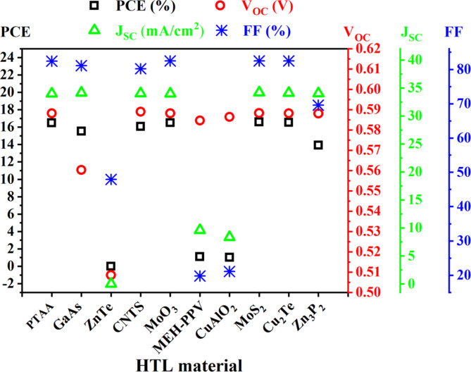
Following the evaluation of various HTL materials on PSCs performance, the device incorporating MoS2 HTL exhibited the highest PCE, as shown in Fig. 2. This superior performance prompted the selection of MoS2 as the HTL for further numerical analysis. A positive VBO (+ 0.15 eV) creates a spike that reduces the carrier recombination and gets a higher efficiency (16.59%) compared to the other HTL.
Fig. 2.
Impact of different HTL materials on device performance.
Band diagram and ETL dependent device performance
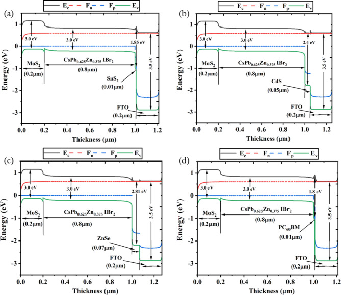
The band alignment of the CsPb.625Zn.375IBr2-based PSC device setup is shown in Fig. 3, where the MoS2 HTL and SnS2, PC60BM, ZnSe, and CdS are utilized as the ETLs. The absorbing layer of each ETL and HTL is used by the valence band offset to be impacted by the energy band diagram and conduction band offset, respectively. The energy level alignment impacts the performance of PSCs. In the PSCs, the flow of electrons is introduced into the matching ETL conduction band while holes are concurrently transported to the HTL91. Subsequently, the corresponding Au and FTO are where holes and electrons are gathered, respectively.
Fig. 3.
Energy band diagram of PSCs with distinct ETLs as (a) SnS2, (b) CdS, (c) ZnSe, (d) PC60BM.
The efficiency of PSCs is profoundly impacted by the energy-level alignment. Photogenerated electrons are simultaneously transported to the HTL by holes and injected into the ETL conduction band in PSCs. Subsequently, the front (FTO) and rear (Au) contact metals accumulate electrons and holes, respectively. The ionization energy of HTL must be less than CsPb.625Zn.375IBr2, and ETL’s electron affinity must be greater than the CsPb.625Zn.375IBr2, to extract the holes at the CsPb.625Zn.375IBr2/HTL interface. Key performance measures of the device, including the JSC, VOC, FF, and PCE, are also profoundly altered by the mismatch in energy bands at the ETL/CsPb.625Zn.375IBr2 and CsPb.625Zn.375IBr2/HTL interface91. The Fermi levels adjacent to the band of valence differ from one another, as Fig. 3 illustrates, but they are in proximity to the conduction band and progressively penetrate it in all four scenarios. Figure 3 displays the energy band map for four distinct solar cell architectures: SnS2, CdS, ZnSe, and PC60BM as ETL. The HTL (MoS2) and the built-in potential of the absorber interface are important factors in influencing the JSC and VOC of PSCs. Electron transport, or the movement of negative charge carriers from the perovskite layer to the electrode, is the function of the ETL. The JSC and VOC as well as the overall performance of the solar cell can be greatly impacted by the kind and quality of the ETL91. An efficient ETL can boost the current density by reducing hole and electron recombination at the contact between the ETL and the perovskite layer91. However, to understand the band alignment between the absorber and different ETLs, it is crucial to analyze the Conduction Band Offset (CBO), which can be calculated as  92. A positive CBO results in a spike-like band alignment, where the absorber’s conduction band is lower than that of the ETL. In contrast, a negative CBO leads to a cliff-like band alignment, where the absorber’s conduction band is higher than the ETL’s. As shown in Fig. 3, most ETL devices exhibit a negative CBO, indicating smoother electron extraction from the absorber to ETL93,94. Due to variations of work function in the ETL and absorber, an almost entirely depleted absorber layer forms in the CsPb.625Zn.375IBr2-based device, as seen in Fig. 3. The passage of charge carriers within the PSCs was influenced by the internal electric field created by this depleted absorber layer. Higher short circuit current (JSC) is the outcome of a fully depleted absorber layer; however, a lower VOC value is caused by an inadequate offset between the absorber/HTL and the quasi-fermi level from the ETL/absorber91.
Optimization of absorber, ETL, and HTL thickness
Impact of absorber thickness
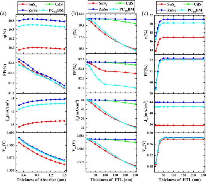
The absorber layer’s thickness has a major impact on how well PSC functions. Figure 4 FTO/ETL/CsPb.625Zn.375IBr2/MoS2/Au PSCs are analyzed with varying absorber, ETL, and HTL thicknesses. Figure 4a illustrates the impact of absorber thickness by varying the absorber’s thickness ranges from 0.5 μm to 1.5 μm. VOC changes ridiculously small when the thickness is varied. When the thickness is 0.5 μm VOC is almost 0.593 V and after increasing the thickness VOC decreases and reaches 0.562 V. This agrees well with values that have been previously published7,95. According to Fig. 4a, JSC rises as absorber thickness increases. The photogeneration of excitons and light absorption are responsible for this increase in JSC. Due to its comparatively poor absorption, a thin absorber layer produces few electron-hole pairs at a large wavelength range. As the perovskite absorber’s thickness expands, the long wavelength absorption rises, improving exciton pair formation. In all four different ETL configurations, JSC is increasing with thickness increments7,95. However, in solar cell configurations, increasing thickness adds to the series resistance, resulting in substantial carrier recombination losses and decreasing FF96. Figure 4 shows that PCE and JSC improve up to 700 nm as the absorber layer thickness grows from 0.2 μm to 1 μm, indicating higher creation of electron-hole pairs97,98. However, an absorber thickness of 0.8 μm has been maintained for further numerical analysis of all ETL devices where the highest PCE, 21.05%, was achieved for the ZnSe ETL device, with a VOC, JSC, and FF of 0.58 V, 43.94 mA/cm2, and 82.17%, respectively.
Fig. 4.
Impact of the absorber, ETL, and HTL thickness on device performance.
Impact of ETL thickness
Extracting electrons from the absorber surface without allowing holes to recombine is the fundamental and main purpose of the ETL. The varying thicknesses of the ETL will alter the visible light transmittance of the film, as demonstrated in experimental settings. Consequently, the thickness of the ETL is especially important for optimizing the solar cell. The fluctuations in ETL thickness from 0.01 μm to 0.25 μm with the output of PSCs may be improved to illustrate the impact of ETL thickness. It is evident from the results shown in Fig. 4b that the PCE reduces as the ETL becomes thicker for SnS2, PC60BM. This reduction may cause more significant pinholes to form, which reduces the JSC. Moreover, a thicker ETL promotes greater electron-hole recombination, increasing resistance and contributing to a decline in PCE99. However, PCE is almost constant for ZnSe and CdS ETL devices and this agrees well with values that have been previously published100. In this study, an ETL thickness of 0.01 μm has been selected as the optimized value for SnS2 and PC60BM-based ETL devices, while thicknesses of 0.05 μm and 0.07 μm are optimized for CdS and ZnSe ETL devices, respectively. These values were maintained in further numerical analyses. Among the four ETL configurations, the ZnSe ETL device achieved the highest PCE of 21.05%, with a VOC, JSC, and FF of 0.58 V, 43.94 mA/cm2, and 82.17%, respectively.
Impact of HTL thickness
Figure 4c illustrates how performance characteristics in CsPb.625Zn.375IBr2-based PSCs utilizing ZnSe, PC60BM, ZnSe, and CdS as ETLs are affected by varying the thickness of the MoS2 HTL. To reduce direct contact between the anode and perovskite and enhance performance, it is imperative to modify the HTL thickness. We exclusively look at MoS2 as the HTL in thickness optimizations. This result suggests that while the device’s charge transport properties improved, there may have been an increase in charge recombination, leading to a relatively stable trend in JSC. As the HTL thickness increases, carrier collection improves, resulting in a rise in Voc. Consequently, an upward trend in PCE is observed. As the HTL increased in thickness of MoS2, Fig. 4c demonstrates that VOC, JSC, FF, and PCE levels remained unchanged for any of the ETLs. Around 21% PCE for ZnSe for 50 nm thickness of MoS2, and this value is consistent with further increments in the thickness of HTL. Similar findings have been reported in previous studies, where an increase in HTL thickness corresponded with enhanced PCE2,7,101–103. However, an HTL thickness of 0.02 μm has been maintained for further numerical analysis across all ETL devices. Notably, the ZnSe ETL device again shows the highest PCE of 21.05%, with a VOC of 0.58 V, JSC of 43.94 mA/cm², and FF of 82.17%.
Optimization of the acceptor, donor, and defect density of the absorber
Impact of acceptor density of absorber
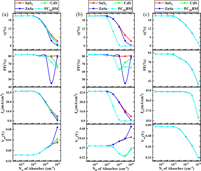
Figure 5a provides descriptive observations on the characteristics of performance following acceptor density (NA) change. NA varies in CsPb.625Zn.375IBr2 absorber from 1 × 1013 cm− 3 to 1 × 1020 cm− 3. Four different ETLs (ZnSe, PC60BM, ZnSe, and CdS) are analyzed here with MoS2 HTL. VOC, JSC, FF, and PCE are merely constant for NA 1 × 1013 cm− 3 to 1 × 1016 cm− 3. So, NA has no influence on cell performance when the value of NA is less than 1 × 1016 cm− 3. However, when the value of NA crosses the value of 1 × 1016 cm− 3, VOC starts to increase but JSC and FF start to decrease, and overall device efficiency starts to decrease. Higher doping concentrations may degrade the solar cell’s active layer by introducing unfavorable shunt pathways through the absorber layer, leading to a reduction in the solar cell’s efficiency104. The same phenomena are observed in previous works95,105. The influence of different types of ETL is limited here. The same characteristics are observed for all types of ETL. However, the optimal absorber acceptor density has been set at 105 cm− 3 across all ETL devices, with the ZnSe ETL device demonstrating comparatively higher performance, achieving a PCE of 21.06%, FF of 82.17%, JSC of 43.94 mA/cm2, and VOC of 0.58 V.
Fig. 5.
Impact of acceptor, acceptor, and donor density of absorber on PSC performance.
Impact of donor density of absorber
Figure 5b illustrates the device performance if the donor density (ND) of absorber CsPb.625Zn.375IBr2 varies from 1 × 1013 cm− 3 to 1 × 1020 cm− 3. To observe the best device configuration for the absorber CsPb.625Zn.375IBr2, MoS2 materials are used for HTL, and four different materials (ZnSe, PC60BM, ZnSe, and CdS) are used to get the best performance. Like NA, the same performance characteristics are absorbed for ND. As the donor density increases, the electric field at the interfaces strengthens, enhancing the charge separation process. However, performance may decline if this stronger field also leads to increased recombination. Additionally, excessive doping can introduce donor defects and increase non-radiative recombination, which may raise the series resistance in PSCs and consequently reduce the PCE. According to Fig. 5b, when the value of ND is higher than 1 × 1016 cm− 3 the PCE starts to diminish. However, for further numerical analysis, the donor density has been set to 105 cm− 3. The ZnSe ETL device demonstrates superior performance among four investigated devices, with a PCE, FF, JSC, and VOC of 21.06%, 82.17%, 43.94 mA/cm2, and 0.58 V respectively.
Impact of defect density of absorber
The absorber defect density (Nt) has a substantial influence on PSC efficacy. Higher Nt levels in the absorber layer cause film degradation and pinhole development, leading to increased recombination and decreased stability and PCE. To determine the optimal defect density, the simulation varied the absorber defect density from 1 × 1013 cm− 3 to 1 × 1018 cm− 3.
The plot of photovoltaic parameters (VOC, JSC, FF, PCE) against perovskite defect density is shown in Fig. 5c. The findings demonstrate that when the CsPb.625Zn.375IBr2 defect density increases, the PCE of the examined PSC device falls. As the fault density increases, VOC reduces linearly, as seen in Fig. 5c. The short diffusion length of the perovskite materials is the cause of this decrease in VOC. The charge carriers are typically trapped by high defect sites in perovskite materials, which shortens their lifespan. Consequently, as this carrier lifetime diminishes, the diffusion length does as well106. Nonetheless, JSC exhibits a constant response up to a defect density of around 1 × 1016 cm− 3, after which it begins to decline as the absorber layer’s defect density increases. This is thus because the JSC is reliant on the pace at which electron-hole pairs are generated. Carrier diffusion is also a factor in JSC, and it gets less with increasing defect density. As a result, JSC falls as fault density increases. However, because of the short diffusion length, it dramatically decreases if the defect density surpasses 1 × 1016 cm− 3107. From this observation, it is observed that up to 1 × 1014 cm− 3 absorber defect density is tolerable beyond this value the performance starts to decrease. The same trends are observed in previously reported articles105,106. Based on the PV parameters, a defect density of 1012 cm− 3 has been selected as the optimal value for further numerical analysis. Under these conditions, the ZnSe ETL device outperforms the other devices, achieving a PCE of 21.05%, FF of 82.17%, JSC of 43.94 mA/cm2, and VOC of 0.58 V.
Optimization of donor and defect density of ETL
Impact of donor density of ETL
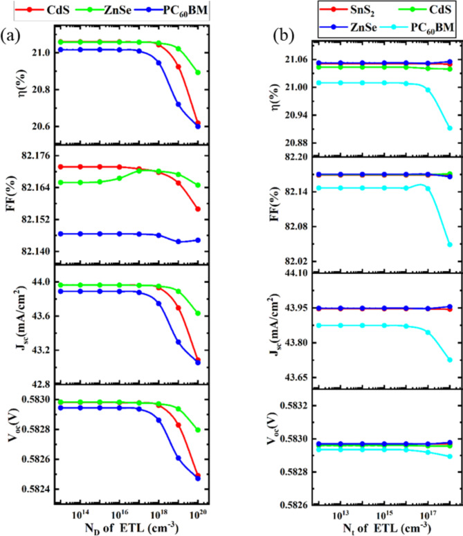
The concentration of doping has a major role in separating the charge carriers produced by photolysis. ETL stops hole migration while transferring electrons to the cathode. The electric field that exists at the ETL/absorber contacts and is dependent on the doping density is what separates these charge carriers108. This electric field at the interfaces can be strengthened by the doping density concentration in ETL layers. Consequently, when the donor density of ETL grows, the minority carrier concentration is considerably reduced at the interfaces due to a reduction in carrier recombination, which raises excitonic separation108,109. To find the best performance, the ETL layer’s doping concentration is changed in this part from 1 × 1013 cm− 3 to 1 × 1020 cm− 3. The output parameters of PSC, are also noted. At a resolution of 1 × 1017 cm− 3, the PSC exhibits optimal performance. It is also evident from Fig. 6a that there is no discernible change in VOC or JSC with the changing of ND of ETL. Keeping the ND in ETL to 1 × 1017 cm− 3 initiates the subsequent assessment procedure and VOC, JSC, FF, and PCE are also nearly dramatically decreased. Similar features are noted in earlier published publications7,110. However, among all devices, the ZnSe ETL device comparatively shows better performance with a PCE, VOC, JSC, and FF of 21.05% 0.58 V, 43.94 mA/cm2, and 82.17%, respectively.
Fig. 6.
Impact of donor and defect density of ETL on device performance.
Impact of defect density of ETL
For various ETLs, the values of VOC, JSC, FF, and PCE are calculated by raising the ETL defect density from 1 × 1012 cm− 3 to 1 × 1018 cm− 3. As the Nt of the ETL increased, Fig. 6b demonstrated that practically all performance parameters—VOC, JSC, FF, and PCE—indicated quite constant values for all ETL layers except PC60BM. When PC60BM is used as ETL all parameters VOC, JSC, FF, and PCE start to decrease when defect density is higher than 1 × 1016 cm− 3. PCE significantly decreases due to an increase in recombination pathways and trap states111. Therefore, a defect density of 1 × 1015 cm− 3 can be considered optimal for better performance in all devices. However, the ZnSe ETL device achieves the highest VOC value of 0.58 V, whereas the JSC value of about 48.94 mA/cm2. PC60BM as the ETL displayed a lower value of JSC (43.87 mA/cm2). The same characteristics are observed in previously reported articles7,95,110.
Optimization of acceptor and defect density of HTL
Impact of acceptor density of HTL
Corresponding to ETL’s donor density, the consequences of HTL’s acceptor density increase the performance of PCSs. The process of separating the charge carriers generated by sunlight is largely dependent on the acceptor concentration. HTL transfers holes to the anode. These charge carriers are distinguished by an electric field that depends on the acceptor density and is present at the absorber/ HTL contacts108. The acceptor density concentration throughout HTL sections can ameliorate the electric field at the interfaces. Consequently, when the acceptor density of HTL increases, fewer carriers recombine at the interfaces, resulting in a significant boost in excitonic separation and a reduction in minority carrier concentration108,109.
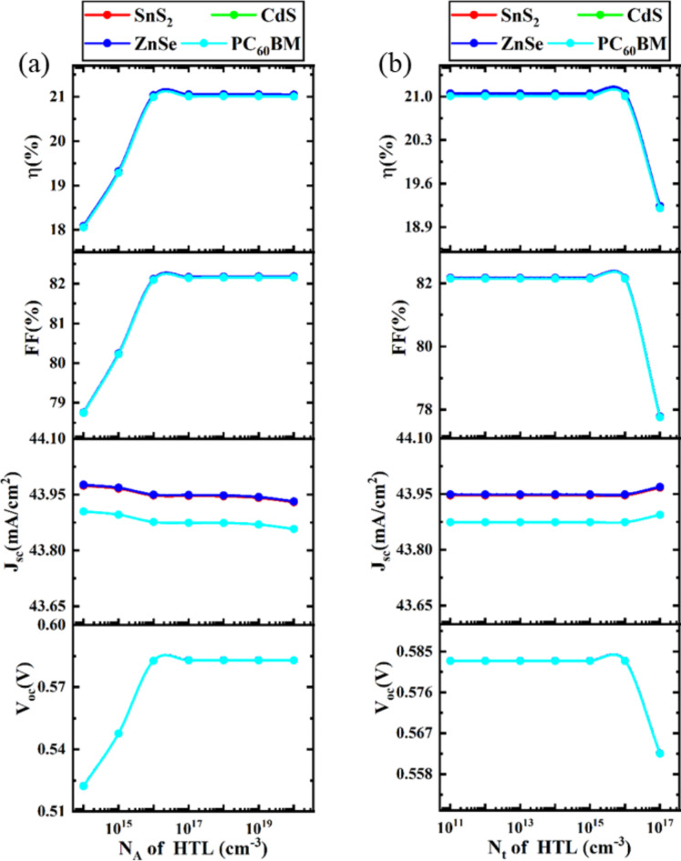
The change in NA of HTL from 1 × 1014 cm− 3 to 1 × 1020 cm− 3, with all other optoelectronic parameters held constant, is shown in Fig. 7a. Up to 1 × 1016 cm− 3 doping density, all the output parameters, such as VOC, FF, and PCE of PSC parameters start increasing while JSC is constant. After increasing acceptor density 1 × 1016 cm− 3, VOC, FF, and PCE remain constant. The optimal value for acceptor doping density is 1 × 1016 cm− 3 since it exhibits the best PCE. By putting this optimization in place, an additional assessment procedure is carried out. Similar features are noted in earlier published publications2,7,110.
Fig. 7.
Impact of acceptor and defect density of HTL on device performance.
Impact of defect density of HTL
The values of VOC, JSC, FF, and PCE are computed for different structures by increasing the HTL defect density from 1 × 1011 cm− 3 to 1 × 1017 cm− 3. Figure 7b showed that almost all performance metrics (VOC, JSC, FF, and PCE) suggested nearly comparable characteristics for all structures when the Nt of the HTL rose. VOC, FF, and PCE are practically constant up to 1 × 1016 cm− 3 defect density; beyond that, they begin to drop, whereas JSC is almost constant or all the density. VOC, FF, and PCE begin to decline at an increase in acceptor density of 1 × 1016 cm− 3, although JSC exhibits very little gain. The primary cause of this PCE deterioration is the rapid formation of numerous recombination sites within the HTL and at the interfaces after exceeding 1 × 1016 cm− 3 of defect density112. This increased defect density in the HTL, caused by factors such as dislocations and native defects, leads to the formation of shallow traps. These traps negatively impact the cell’s performance by acting as non-radiative recombination centers113. Given that it has the best PCE, 1 × 1016 cm− 3 is the ideal acceptor doping density. By implementing this optimization, a further evaluation process is completed. Similar characteristics have been reported in past publications7,95.
Effects of series resistance, shunt resistance, and temperature
Impact of series resistance on device performance
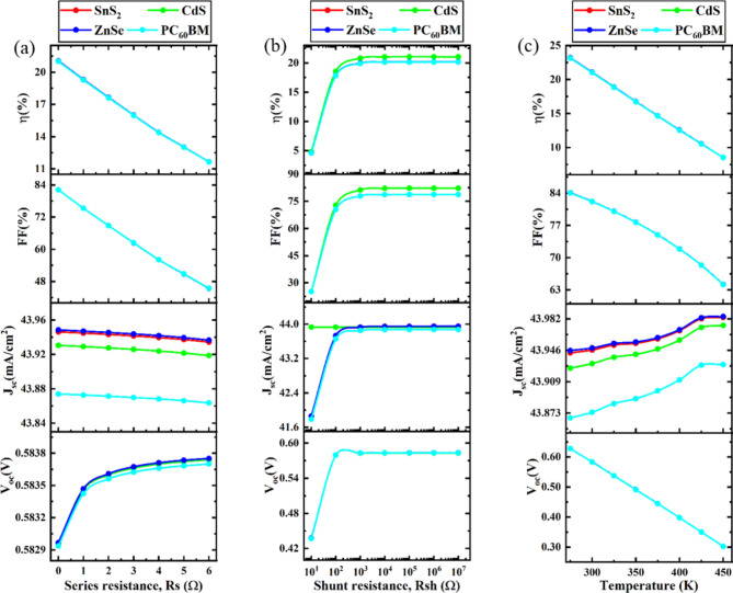
The combination of the absorber layer resistance and the ohmic contact resistance of the device is known as series resistance (RS). The impact of varying the series resistance for four different ETLs (ZnSe, PC60BM, ZnSe, and CdS)-associated structures from 0 Ω-cm2 to 6 Ω-cm2 is examined, as shown in Fig. 8a. It is shown that JSC and VOC were almost unaffected by increasing RS. Nonetheless, the growth in RS has resulted in an enormous downturn in the FF (82–44%) and PCE (21–12%) for all structures. Consequently, throughout the device’s manufacture, RS must be reduced to a minimum to maximize performance and optimize FF. To reduce RS, decreasing the thickness of the absorber layer during manufacturing is not a solution because of lowering the thickness of the absorber layer, as doing so causes a noncomplementary absorption30,110. Minimizing the resistance to contact between the electrodes and active layer or designing well-interacting donor-acceptor interfaces are two further experimental techniques to reduce RS30,110. A similar output trend is noted in earlier published publications114,115.
Fig. 8.
Impact of series resistance, shunt resistance, and temperature on device performance.
Impact of shunt resistance on device performance
Materials for absorbers, interface barriers, interlayers that gather charges, and electrodes all contribute to PSCs’ internal resistance. The Shockley equation (Eqs. 13–14) describes how a solar cell’s J-V characteristic responds under ideal one-sun illumination parameters30,110,114.
 |
13 |
……….
 |
14 |
…………
The equation includes the elementary charge (qe), photocurrent density (JPH), reverse bias saturation current density (Jo), series resistance (RS), shunt resistance (RSh), diode ideality factor (n), Boltzmann constant (1.38 × 10²³ JK− 1), and ambient temperature (298 K).
Figure 8b illustrates how VOC, JSC, FF, and PCE values affect RSh variation, which ranges from 10 Ω-cm27 to 10 Ω-cm2 for all PSC configurations. As RSh rose, the PV parameters followed a comparable pattern, rapidly rising from 10 Ω-cm23 to 10 Ω-cm2. According to Fig. 8b, different ETL-associated structures had the same VOC of 0.58 V. Figure 8b shows that ZnSe, PC60BM, ZnSe, and CdS as ETL structures, JSC increased with the fluctuation of RSh for different ETL-associated structures. After 103 Ω-cm2, the JSC for RSh increased in all PSC structures and remained steady. As for FF, Fig. 8b indicates that all four PSC structures exhibited a rising trend; however, once RSh variation decreased, CdS, ETL-associated PSC structures, displayed about 80% FF. The remaining four PSC structures linked to ETLs exhibited less than 80% of FF. According to Fig. 8b, nearly the same trend was seen in the PCE cases of CdS, where the structure connected to the ETL has an enhanced PCE of about > 20%. A similar output trend is noted in earlier published publications114,115. Thus, this analysis indicates that maximizing shunt resistance is essential for achieving optimal device performance.
Impact of temperature on device performance
The power output of a PSC is directly impacted by its operating temperature. Higher operating temperatures are expected to have an impact on the density of states, band gaps, electron and hole mobility, carrier concentrations, and other solar cell properties2. Similarly, the operating temperature impacts the proposed cell’s performance parameters. The temperature of this simulation impact is adjusted between 275 k and 450 K. Figure 8C displays the VOC plotted against temperature fluctuation. The graph shows that when the working temperature of the cell rises, the VOC falls, though JSC remains almost constant. The creation of extra interfacial defects, a rise in series resistance, and a short carrier diffusion length may all be employed to clarify the decline in VOC according to the operational temperature2. FF and PCE of the raised four models also start decreasing with an increment in temperature. According to our findings, the greatest PCE is produced under the usual test setting of 300 K, and the PCE declines linearly when the temperature escalates. The approximate PCE of the suggested cell at 300 K is 21.05% for the CdS- ETL-based PSC structure. The same phenomenon is noted in earlier published publications116,117.
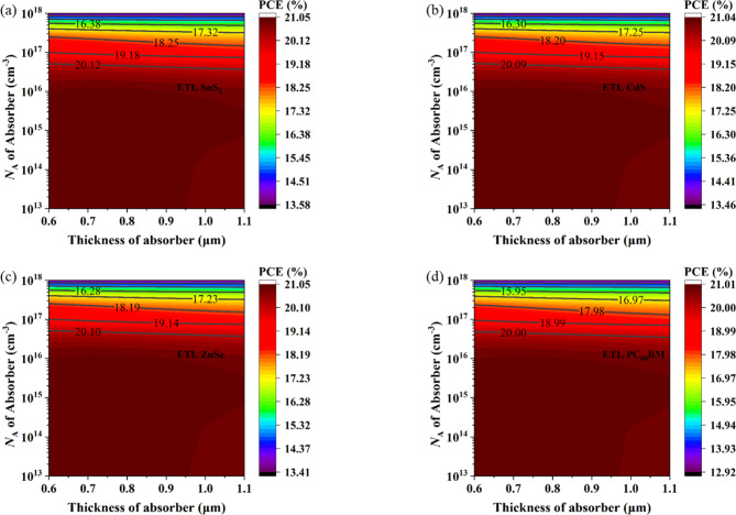
Effect of absorber layer thickness with absorber acceptor density
The absorber layer thickness and acceptor are critical factors impacting device performance. Optimizing these parameters is necessary to get optimal performance. During simulation, the absorber thickness was adjusted from 0.5 μm to 1.5 μm, and the NA was modified from 1 × 1013 cm− 3 to 1 × 1020 cm− 3 to examine the effects of these factors on the PV performance characteristics of the four optimized PSCs. The impact of simultaneously varying the thickness of the absorber layer and NA using contour plot mapping is seen in Fig. 9 on the PCE for the buildings under investigation. It is pleasing to note that when the thickness of the absorber was modified using absorber NA, SnS2, PC60BM, ZnSe, and CdS ETL-based PSC structures displayed almost similar patterns. When both the NA and absorber thickness are less extensive than 1 × 1016 cm− 3 and 0.95 μm, respectively, the maximum PCE (~ 21.05%) was observed in these four solar structures. Additionally, ZnSe and CdS as the ETL have the most prominent PCE among the four optimized PSCs, whereas PC60BM exhibits the lowest PCE. Therefore, it can be said that for CsPb.625Zn.375IBr2 absorber-based PSCs, it is better to employ inorganic oxide-based ETLs rather than organic ones.
Fig. 9.
Correlation between absorber acceptor density and absorber layer thickness.
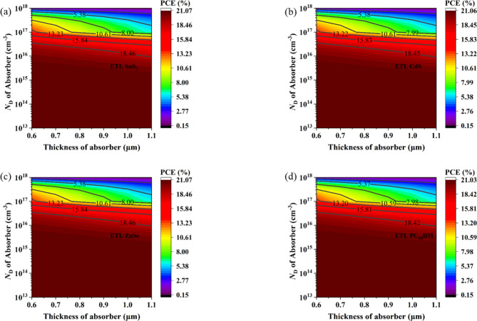
Effect of absorber layer thickness with absorber donor density
This work uses contour mapping to examine how adjusting the absorber donor density and width of the absorber layer affects the performance of the CsPb.625Zn.375IBr2 absorber-based PSCs. When ND is less than 1 × 1016 cm− 3 and the absorber thickness is 0.6 μm to 1.1 μm, the PCE is at its highest (> 21%). When ND rises more than 1 × 1016 cm− 3, PCE starts to fall as well, but absorber layer thickness has no impact on PCE. As Fig. 10 shows, the maximum value of PCE (21.07%) can be obtained using SnS2 and ZnSe ETL-based PSC structures whereas PC60BM exhibits the lowest PCE. Therefore, it can be said that for CsPb.625Zn.375IBr2 absorber-based PSCs, it is better to employ inorganic oxide-based ETLs rather than organic ones.
Fig. 10.
Effect of absorber layer thickness with absorber donor density.
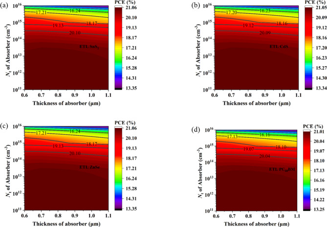
Effect of absorber layer thickness with absorber defect density
The absorber thickness and defect density have a major direct impact on the Solar cell performance. Increased recombination lowers the PCE of PSCs because greater Nt in the absorber layer causes pinhole formation and film breakdown30,110. By adjusting the absorber depth between 0.6 μm and 1.1 μm, the simulation was run to determine the most beneficial defect density for a given absorber layer thickness and Nt adjusted between 1 × 1011 cm− 3 to 1 × 1016 cm− 3. For every building under investigation, Fig. 11 shows variations in absorber layer thickness and Nt, which cause PCE to fluctuate. Figure 11 illustrates how variations in absorber thickness and Nt affect PCE. As ETL-based solar structures, SnS2, PC60BM, ZnSe, and CdS exhibit a comparable pattern for the PCE value with adjustments to Nt and absorber thickness, as shown in Fig. 11. Out of all the devices under study, SnS2 and ZnSe, as the ETL demonstrated the maximum PCE of around 21.05% happens when the absorber depth ranges from 0.6 μm to 1.1 μm and defect density, is less than 2 × 1013 cm− 3. In the presence of a defect, inorganic ETLs (SnS2, ZnSe, and CdS) based PSCs outperform the organic ETLs-based PSCs.
Fig. 11.
Effect of absorber layer thickness with absorber defect density.
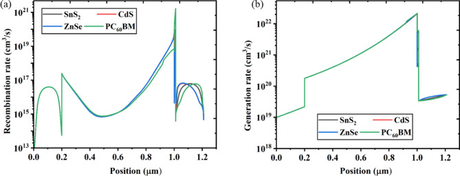
Effect of generation rate and recombination rate
The coupling and annihilation of electrons and holes in the conduction band is the process of recombination. The lifespan and charge carrier density both have an impact on the recombination rate. Furthermore, the electron-hole recombination is affected by every defect condition present in the several PSC layers95. The four PSCs had a maximum recombination rate that was like the generation rate, within 1.0 μm, as seen in Fig. 12a. The region between 1.0 μm displayed an elevated recombination rate due to more conduction band electrons crossing the energy barrier, entering the valence band, and becoming more stable by taking the position of the valence band hole. The consequence of energy levels influences the electron hole’s recombination rate inside the device, and imperfection and grain boundaries may cause the recombination rate distribution in the solar architecture to be non-uniform95.
Fig. 12.
Effect of generation rate and recombination rate.
The generated electron-hole pair may be found for any wavelength of light, the whole conventional solar spectrum, and at any position within the solar cell. The largest generation rate is near the device surface, where most of the light is absorbed30,110. The generation rate of a solar cell indicates the quantity of electron-hole pairs produced inside the device as a result of photon absorption at a certain wavelength., which depends on both position and wavelength. The generation rate is essential for PSCs to operate as efficiently as possible. The four optimized solar devices’ generating rates are displayed in Fig. 12b. As the figure makes clear, all four different structure PSCs based on SnS2, ZnSe, PC60BM, and CdS ETLs demonstrated generation rates start increasing from 0.2 μm and reached greater generation rate at PSC depths of 1.0 μm.
JV and QE characteristics curve
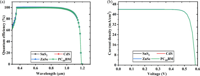
The quantity of current produced by photoirradiation at a certain wavelength is known as a perovskite solar cell’s quantum efficiency (QE)118,119. The number of charge carriers that are moved and gathered by the electrodes can also be used to calculate the QE. The ideal form of a solar cell’s QE curve is square or rectangular; however, it can be distorted by factors such as surface passivation, recombination, and reflection losses49,103. For the solar cell architectures of FTO/SnS2/CsPb.625Zn.375IBr2/MoS2/Au, FTO/ZnSe/CsPb.625Zn.375IBr2/MoS2/Au, FTO/CdS/CsPb.625Zn.375IBr2/MoS2/Au and FTO/PC60BM/CsPb.625Zn.375IBr2/MoS2/Au, the nature of QE for varying wavelength is investigated to more precisely recognize the accumulation of charge carriers. The QE curves for both solar cell architectures are displayed in Fig. 13a before the optimization condition. Figure 13a illustrates that all four structures have a QE of 100% at 400 nm. However, QE begins to decline after 1000 nm wavelength in all cases of structures. The QE graph is square and deemed excellent when the QE value remains constant over the observed wavelength range. The QE of the PSC is lowered due to the recombination, even if the charge carriers cannot go into an external circuit. For most solar cells, recombination lowers QE while charge carriers are incapable of an external circuit. The same factors that affect collection probability also affect QE. Modifying the front surface, for instance, may affect carriers formed close to the surface. Longer wavelength QE can be decreased by the absorbance of free carriers from front surface layers that are highly doped.
Fig. 13.
JV and QE characteristics curve.
The J-V characteristic curve of the PSCs architectures including FTO/SnS2/CsPb.625Zn.375IBr2/MoS2/Au, FTO/ZnSe/CsPb.625Zn.375IBr2/MoS2/Au, FTO/CdS/CsPb.625Zn.375IBr2/MoS2/Au and FTO/PC60BM/CsPb.625Zn.375IBr2/MoS2/Au are shown in Fig. 13b. As seen in Fig. 13b, all four PSC structures displayed a JSC of about 44 mA/cm2 when the VOC was around 0.58 V. Defect states in perovskite films led to a considerable drop in all photovoltaic metrics. This is in line with studies showing that perovskite’s notable crystallization improves its functioning and diminishes charge recombination.
Conclusion
This work thoroughly examines several CsPb.625Zn.375IBr2 -based PSC features with varying HTLs and ETLs. Through an examination of key variables influencing PSC performance, the study seeks to identify the optimal design for maximizing conversion efficiency. According to the study, the following elements are crucial for maximizing PSC performance:
1. First of all, we analyzed different types of HTL materials for CsPb.625Zn.375IBr2 -based PSC, and the best HTL materials for CsPb.625Zn.375IBr2 -based PSC is MoS2.
2. Device performance is significantly impacted by the thickness of the absorber, ETL, and HTL. We found that 800 nm thick absorber layer, 100 nm thick ETL layer, and 50 nm thick HTL layer help us to get the best result.
3. To get the optimum performance we need to set both the acceptor density and donor density of the absorber to less than 1 × 1016 cm-3 and defect density should not be higher than 1 × 1014 cm-3.
4. The density of HTL acceptors and ETL donors should be less than 1 × 1017 cm-3 and the defect density should be less than 1 × 1015 cm-3.
5. Shunt resistance enhances PCE and FF and has negligible effects on JSC and VOC, while an increase in series resistance drastically reduces PCE.
In summary, our thorough analysis shows that several factors, including properties of the ETL and HTL, the width of the absorber layer, acceptor density, and defect densities, influence the performance of CsPb.625Zn.375IBr2 -based PSCs. By optimizing these parameters, PCEs of 21.05% for the FTO/ZnSe/CsPb.625Zn.375IBr2/MoS2/Au structures and 21.04% for the FTO/CdS/CsPb.625Zn.375IBr2/MoS2/Au structures are obtained. By laying the groundwork for future improvements in stability and efficiency, these optimized designs prepare the ground for using CsPb.625Zn.375IBr2 -based PSCs in renewable energy applications.
Acknowledgements
The authors gratefully acknowledge Dr. M. Burgelman of the University of Gent, Belgium, for providing the SCAPS-1D program (version 3.3.10) used in this research. The software is available at https://scaps.elis.ugent.be/. The authors would like to express their gratitude to him. This work was funded by the Researchers Supporting Project Number (RSP2024R265) King Saud University, Riyadh, Saudi Arabia.
Author contributions
M.K. Hossain: Conceptualization, Methodology, Software, Validation, Formal analysis, Investigation, Data curation, Writing – original draft, Writing – review & editing, Supervision, Project administration; M.A. Islam: Formal analysis, Writing – original draft; M.S. Uddin: Software, Validation, Formal analysis, Investigation, Data curation; P. Paramasivam: Validation, Investigation, Formal analysis, Writing – review & editing; J.A. Hamid, R.A. Alshgari, V. K. Mishra, and R. Haldar: Validation, Formal analysis, Writing – review & editing.
Data availability
The datasets used and/or analysed during the current study available from the corresponding author on reasonable request.
Declarations
Competing interests
The authors declare no competing interests.
Footnotes
Publisher’s note
Springer Nature remains neutral with regard to jurisdictional claims in published maps and institutional affiliations.
Contributor Information
M. Khalid Hossain, Email: khalid.baec@gmail.com, Email: khalid@kyudai.jp.
Prabhu Paramasivam, Email: prabhu.paramasivam@meu.edu.et.
V. K. Mishra, Email: mishravlm30@gmail.com
Rajesh Haldhar, Email: rajeshhaldhar.lpu@gmail.com.
References
- 1.Kang, J. & Cho, J. H. Organic-inorganic hybrid perovskite electronics. Phys. Chem. Chem. Phys.22, 13347–13357 (2020). [DOI] [PubMed] [Google Scholar]
- 2.Chakrabartty, J., Islam, M. A. & Reza, S. Performance analysis of highly efficient 2D/3D bilayer inverted perovskite solar cells. Sol Energy. 230, 195–207 (2021). [Google Scholar]
- 3.Hossain, M. K. et al. Exploring the optoelectronic and photovoltaic characteristics of lead-free Cs2TiBr6 double perovskite solar cells: a DFT and SCAPS‐1D investigations. Adv. Electron. Mater.10.1002/aelm.202400348 (2024). [Google Scholar]
- 4.Hossain, M. K. et al. Design insights into La2NiMnO6-based perovskite solar cells employing different charge transport layers: DFT and SCAPS-1D frameworks. Energy Fuels. 37, 13377–13396 (2023). [Google Scholar]
- 5.Roy, P., Kumar Sinha, N., Tiwari, S. & Khare, A. A review on perovskite solar cells: evolution of architecture, fabrication techniques, commercialization issues and status. Sol Energy. 198, 665–688 (2020). [Google Scholar]
- 6.Tailor, N. K. et al. Recent progress in morphology optimization in perovskite solar cell. J. Mater. Chem. A8, 21356–21386 10.1039/d0ta00143k (2020).
- 7.Hossain, M. K. et al. High-efficiency lead-free La2NiMnO6-based double perovskite solar cell by incorporating charge transport layers composed of WS2, ZnO, and Cu2FeSnS4. Energy Fuels. 37, 19898–19914 (2023). [Google Scholar]
- 8.Uddin, M. S. et al. An in-depth investigation of the combined optoelectronic and photovoltaic properties of lead‐free Cs2AgBiBr6 double perovskite solar cells using DFT and SCAPS‐1D frameworks. Adv. Electron. Mater.10, 2300751 (2024).
- 9.A, K. et al. Organometal halide perovskites as visible-light sensitizers for photovoltaic cells. J. Am. Chem. Soc.131, 6050–6051 (2009). [DOI] [PubMed] [Google Scholar]
- 10.NREL. Best Research-Cell Efficiency Chart | Photovoltaic Research | NREL. (2023).
- 11.Hossain, M. K. et al. An extensive study on charge transport layers to design and optimization of high-efficiency lead-free Cs2PtI6-based double-perovskite solar cells: a numerical simulation approach. Results Phys.61, 107751 (2024). [Google Scholar]
- 12.Grancini, G. & Nazeeruddin, M. K. Dimensional tailoring of hybrid perovskites for photovoltaics. Nat. Rev. Mater. 4, 4–22 10.1038/s41578-018-0065-0 (2019).
- 13.Chakrabartty, J., Harnagea, C., Celikin, M., Rosei, F. & Nechache, R. Improved photovoltaic performance from inorganic perovskite oxide thin films with mixed crystal phases. Nat. Photonics. 12, 271–276 (2018). [Google Scholar]
- 14.Song, Z. et al. Perovskite solar cell stability in humid air: partially reversible phase transitions in the PbI 2 -CH 3 NH 3 I‐H 2 O system. Adv. Energy Mater.6, 1600846 (2016). [Google Scholar]
- 15.Tiep, N. H., Ku, Z. & Fan, H. J. Recent advances in improving the stability of perovskite solar cells. Adv. Energy Mater.6, (2016).
- 16.Salhi, B., Wudil, Y. S., Hossain, M. K., Al-Ahmed, A. & Al-Sulaiman, F. A. Review of recent developments and persistent challenges in stability of perovskite solar cells. Renew. Sustain. Energy Rev. 90, 210–222 10.1016/j.rser.2018.03.058 (2018).
- 17.Wang, R. et al. A review of perovskites solar cell stability. Adv. Funct. Mater.29, 1808843 (2019). [Google Scholar]
- 18.Ortiz-Cervantes, C., Carmona-Monroy, P. & Solis-Ibarra, D. Two-dimensional halide perovskites in solar cells: 2D or not 2D? ChemSusChem12, 1560–1575 10.1002/cssc.201802992 (2019). [DOI] [PubMed]
- 19.Yan, J., Qiu, W., Wu, G., Heremans, P. & Chen, H. Recent progress in 2D/quasi-2D layered metal halide perovskites for solar cells. Journal of Materials Chemistry A6, 11063–11077 10.1039/c8ta02288g (2018).
- 20.Tai, Q., Tang, K. C. & Yan, F. Recent progress of inorganic perovskite solar cells. Energy Environ. Sci.12, 2375–2405 10.1039/c9ee01479a (2019).
- 21.Ma, C. et al. 2D/3D perovskite hybrids as moisture-tolerant and efficient light absorbers for solar cells. Nanoscale8, 18309–18314 (2016). [DOI] [PubMed] [Google Scholar]
- 22.Duan, J. et al. Inorganic perovskite solar cells: an emerging member of the photovoltaic community. J. Mater. Chem. A. 7, 21036–21068 (2019). [Google Scholar]
- 23.Wang, J. et al. Highly efficient all-inorganic perovskite solar cells with suppressed non-radiative recombination by a Lewis base. Nat. Commun.11, 177 (2020). [DOI] [PMC free article] [PubMed] [Google Scholar]
- 24.Liu, X. et al. Boosting the efficiency of carbon-based planar CsPbBr3 perovskite solar cells by a modified multistep spin-coating technique and interface engineering. Nano Energy. 56, 184–195 (2019). [Google Scholar]
- 25.Zhang, J., Hodes, G., Jin, Z. & Liu, S. All-inorganic CsPbX3 perovskite solar cells: progress and prospects. Angewandte Chemie - International Edition58, 15596–15618 10.1002/anie.201901081 (2019). [DOI] [PubMed]
- 26.Zeng, Q. et al. Inorganic CsPbI2Br perovskite solar cells: the progress and perspective. Sol RRL3, (2019).
- 27.Yuan, Y., Yan, G., Hong, R., Liang, Z. & Kirchartz, T. Quantifying efficiency limitations in all-inorganic halide perovskite solar cells. Adv. Mater.3410.1002/adma.202108132 (2022). [DOI] [PubMed]
- 28.Maafa, I. M. All-Inorganic perovskite solar cells: recent advancements and challenges. Nanomaterials1210.3390/nano12101651 (2022). [DOI] [PMC free article] [PubMed]
- 29.Chen, H. et al. Inorganic perovskite solar cells: a rapidly growing field. Solar RRL210.1002/solr.201700188 (2018).
- 30.Hossain, M. K. et al. Numerical Analysis in DFT and SCAPS-1D on the influence of different charge transport layers of CsPbBr3 perovskite solar cells. Energy Fuels. 37, 6078–6098 (2023). [Google Scholar]
- 31.Kaur, N. et al. Low lead inorganic Zn-based mixed-halide perovskites CsPb 0.625 Zn 0.375 I 3–β X β (X = cl or br) for energy generation with 23.5% efficiency. Phys. Scr.98, 115941 (2023). [Google Scholar]
- 32.Kaur, N., Madan, J. & Pandey, R. Numerical simulation study of CsPb0.625Zn0.375IBr2 perovskite solar cell. Mater. Today Proc.10.1016/j.matpr.2023.03.367 (2023).
- 33.Lee, S. et al. Inorganic narrow bandgap CsPb0.4Sn0.6I2.4Br0.6 perovskite solar cells with exceptional efficiency. Nano Energy. 77, 105309 (2020). [Google Scholar]
- 34.Liang, J. et al. CsPb0.9Sn0.1IBr2 based all-inorganic perovskite solar cells with exceptional efficiency and stability. J. Am. Chem. Soc.139, 14009–14012 (2017). [DOI] [PubMed] [Google Scholar]
- 35.Yang, F. et al. All-inorganic CsPb1 – GeI2Br perovskite with enhanced phase stability and photovoltaic performance. Angew Chemie Int. Ed.57, 12745–12749 (2018). [DOI] [PubMed] [Google Scholar]
- 36.Li, N., Zhu, Z., Li, J., Jen, A. K. Y. & Wang, L. Inorganic CsPb1 – SnIBr2 for efficient wide-bandgap perovskite solar cells. Adv. Energy Mater.8, 1800525 (2018). [Google Scholar]
- 37.Yaghoobi Nia, N. et al. Impact of P3HT regioregularity and molecular weight on the efficiency and stability of perovskite solar cells. ACS Sustain. Chem. Eng.9, 5061–5073 (2021). [Google Scholar]
- 38.Salim, T. et al. Perovskite-based solar cells: impact of morphology and device architecture on device performance. J. Mater. Chem. A. 3, 8943–8969 (2015). [Google Scholar]
- 39.Diau, E. W. G., Jokar, E. & Rameez, M. Strategies to improve performance and stability for tin-based perovskite solar cells. ACS Energy Lett.4, 1930–1937 10.1021/acsenergylett.9b01179 (2019).
- 40.Pascual, J. et al. Lights and shadows of DMSO as solvent for tin halide perovskites. Chem. – Eur. J.28, e202103919 (2022). [DOI] [PMC free article] [PubMed] [Google Scholar]
- 41.Aygan Atesin Sajid Bashir Jingbo Louise Liu & Editors, T. Nanostructured Materials for Next-Generation Energy Storage and Conversion10.1007/978-3-662-59594-7 (Springer, 2019).
- 42.Ghosh, R., Singh, A. & Agarwal, P. Study on effect of different HTL and ETL materials on the perovskite solar cell performance with TCAD simulator. Mater. Today Proc.10.1016/J.MATPR.2023.06.161 (2023).34178606 [Google Scholar]
- 43.Bichave, S., Mundupuzhakal, J., Gajjar, P. N. & Gupta, S. K. Analysis of varying ETL/HTL material for an effective perovskite solar cell by numerical simulation. Mater. Today Proc.10.1016/J.MATPR.2023.01.190 (2023). [Google Scholar]
- 44.Jamal, S., Khan, A. D. & Khan, A. D. High performance perovskite solar cell based on efficient materials for electron and hole transport layers. Optik (Stuttg)218, (2020).
- 45.Fatema, K. & Arefin, M. S. Enhancing the efficiency of Pb-based and Sn-based perovskite solar cell by applying different ETL and HTL using SCAPS-ID. Opt. Mater. (Amst). 125, 112036 (2022). [Google Scholar]
- 46.Prochowicz, D. et al. Suppressing recombination in perovskite solar cells via surface engineering of TiO2 ETL. Sol Energy. 197, 50–57 (2020). [Google Scholar]
- 47.Tavakoli, M. M., Yadav, P., Tavakoli, R. & Kong, J. Surface engineering of TiO2 ETL for highly efficient and hysteresis-less planar perovskite solar cell (21.4%) with enhanced open-circuit voltage and stability. Adv. Energy Mater.8, (2018).
- 48.Lin, L. et al. Inorganic electron transport materials in perovskite solar cells. Adv. Funct. Mater.3110.1002/adfm.202008300 (2021).
- 49.Rai, N., Rai, S., Singh, P. K., Lohia, P. & Dwivedi, D. K. Analysis of various ETL materials for an efficient perovskite solar cell by numerical simulation. J. Mater. Sci. Mater. Electron.31, 16269–16280 (2020). [Google Scholar]
- 50.Abulikemu, M., Barbé, J., Labban, E., Eid, A., Del Gobbo, S. & J. & Planar heterojunction perovskite solar cell based on CdS electron transport layer. Thin Solid Films. 636, 512–518 (2017). [Google Scholar]
- 51.Patil, P. et al. Hybrid interfacial ETL engineering using PCBM-SnS2 for high-performance p-i-n structured planar perovskite solar cells. Chem. Eng. J.397, 125504 (2020). [Google Scholar]
- 52.Benali, H. et al. Synthesis and characterization of Mg-doped ZnO thin-films for photovoltaic applications. Mater. Today Proc.66, 212–216 (2022).
- 53.Li, X. et al. Thermally evaporated ZnSe for efficient and stable regular/inverted perovskite solar cells by enhanced electron extraction. ENERGY Environ. Mater.6, e12439 (2023). [Google Scholar]
- 54.Namkoong, G., Mamun, A. A. & Ava, T. T. Impact of PCBM/C60 electron transfer layer on charge transports on ordered and disordered perovskite phases and hysteresis-free perovskite solar cells. Org. Electron.56, 163–169 (2018). [Google Scholar]
- 55.Li, S., Cao, Y. L. Y. L., Li, W. H. W. H. & Bo, Z. S. Z. S. A brief review of hole transporting materials commonly used in perovskite solar cells. Rare Met.40, 2712–2729 (2021). [Google Scholar]
- 56.Pitchaiya, S. et al. A review on the classification of organic/inorganic/carbonaceous hole transporting materials for perovskite solar cell application. Arab. J. Chem.13, 2526–2557 10.1016/j.arabjc.2018.06.006 (2020).
- 57.Shariatinia, Z. Recent progress in development of diverse kinds of hole transport materials for the perovskite solar cells: A review. Renew. Sustain. Energy Rev.11910.1016/j.rser.2019.109608 (2020).
- 58.Murugan, P., Hu, T., Hu, X. & Chen, Y. Advancements in organic small molecule holetransporting materials for perovskite solar cells: Past and future. J. Mater. Chem. A 10, 5044–5081 10.1039/d1ta11039j (2022).
- 59.Wang, J. M. et al. Small molecule-polymer composite hole-transporting layer for highly efficient and stable perovskite solar cells. ACS Appl. Mater. Interfaces. 9, 13240–13246 (2017). [DOI] [PubMed] [Google Scholar]
- 60.Vasilopoulou, M. et al. Molecular materials as interfacial layers and additives in perovskite solar cells. Chem. Soc. Rev.49, 4496–4526 10.1039/c9cs00733d (2020). [DOI] [PubMed]
- 61.Elseman, A. M., Sajid, S., Shalan, A. E., Mohamed, S. A. & Rashad, M. M. Recent progress concerning inorganic hole transport layers for efficient perovskite solar cells. Appl. Phys. A Mater. Sci. Process.12510.1007/s00339-019-2766-7 (2019).
- 62.Arumugam, G. M. et al. Inorganic hole transport layers in inverted perovskite solar cells: a review. Nano Sel.2, 1081–1116 (2021). [Google Scholar]
- 63.Kung, P. K. et al. A review of inorganic hole transport materials for perovskite solar cells. Adv. Mater. Interfaces. 510.1002/admi.201800882 (2018).
- 64.Hossain, M. K. et al. Enhancing efficiency and performance of Cs2TiI6-based perovskite solar cells through extensive optimization: a numerical approach. Inorg. Chem. Commun.168, 112964 (2024). [Google Scholar]
- 65.Et-taya, L., Ouslimane, T. & Benami, A. Numerical analysis of earth-abundant Cu2ZnSn(SxSe1-x)4 solar cells based on spectroscopic ellipsometry results by using SCAPS-1D. Sol Energy. 201, 827–835 (2020). [Google Scholar]
- 66.Hossain, M. K. et al. Influence of natural dye adsorption on the structural, morphological and optical properties of TiO2 based photoanode of dye-sensitized solar cell. Mater. Sci.36, 93–101 (2017). [Google Scholar]
- 67.Hossain, M. K., Rahman, M. T., Basher, M. K., Manir, M. S. & Bashar, M. S. Influence of thickness variation of gamma-irradiated DSSC photoanodic TiO2 film on structural, morphological and optical properties. Optik (Stuttg). 178, 449–460 (2019). [Google Scholar]
- 68.Hossain, M. K. et al. Efficiency enhancement of natural dye sensitized solar cell by optimizing electrode fabrication parameters. Mater. Sci.35, 816–823 (2017). [Google Scholar]
- 69.Hossain, M. K., Rahman, M. T., Basher, M. K., Afzal, M. J. & Bashar, M. S. Impact of ionizing radiation doses on nanocrystalline TiO2 layer in DSSC’s photoanode film. Results Phys.11, 1172–1181 (2018). [Google Scholar]
- 70.Rani, S., Kumar, A. & Ghosh, D. S. Optical designing of perovskite solar cells. 10.1109/JPHOTOV.2022.3141344 (2022).
- 71.Rani, S., Kumar, A. & Sundar Ghosh, D. High performance of NiO-Ag-NiO based semi-transparent perovskite solar cell. Mater. Today Proc.66, 3224–3227 (2022).
- 72.Basher, M. K., Hossain, M. K., Uddin, M. J., Akand, M. A. R. & Shorowordi, K. M. Effect of pyramidal texturization on the optical surface reflectance of monocrystalline photovoltaic silicon wafers. Optik (Stuttg). 172, 801–811 (2018). [Google Scholar]
- 73.Hossain, M. I. et al. Effect of back reflectors on photon absorption in thin-film amorphous silicon solar cells. Appl. Nanosci.7, 489–497 (2017). [Google Scholar]
- 74.Basher, M. K. et al. Study and analysis the Cu nanoparticle assisted texturization forming low reflective silicon surface for solar cell application. AIP Adv.9, 1–6 (2019). [Google Scholar]
- 75.Basher, M. K., Hossain, M. K. & Akand, M. A. R. Effect of surface texturization on minority carrier lifetime and photovoltaic performance of monocrystalline silicon solar cell. Optik (Stuttg). 176, 93–101 (2019). [Google Scholar]
- 76.Singh, N., Agarwal, A. & Agarwal, M. Performance evaluation of lead–free double-perovskite solar cell. Opt. Mater. (Amst). 114, 110964 (2021). [Google Scholar]
- 77.Singh, N. K., Agarwal, A. & Kanumuri, T. Performance enhancement of environmental friendly ge-based perovskite solar cell with zn 3 P 2 and SnS 2 as charge transport layer materials. Energy Technol.10, 2100782 (2022). [Google Scholar]
- 78.Bansal, S. & Aryal, P. Evaluation of new materials for electron and hole transport layers in perovskite-based solar cells through SCAPS-1D simulations. In Conf. Rec. IEEE Photovolt. Spec. Conf. 747–750 (2016).
- 79.Raza, E. et al. Numerical simulation analysis towards the effect of charge transport layers electrical properties on cesium based ternary cation perovskite solar cells performance. Sol Energy. 225, 842–850 (2021). [Google Scholar]
- 80.Qasim, I. et al. Numerical optimization of (FTO/ZnO/CdS/CH3NH3SnI3/GaAs/Au) perovskite solar cell using solar capacitance simulator with efficiency above 23% predicted. Opt. Quantum Electron.53, 713 (2021). [Google Scholar]
- 81.Singh, N. K. & Agarwal, A. Performance assessment of sustainable highly efficient CsSn0.5Ge0.5I3/FASnI3 based perovskite solar cell: a numerical modelling approach. Opt. Mater. (Amst). 139, 113822 (2023). [Google Scholar]
- 82.Khan, Z., Noman, M., Tariq Jan, S. & Daud Khan, A. Systematic investigation of the impact of kesterite and zinc based charge transport layers on the device performance and optoelectronic properties of ecofriendly tin (sn) based perovskite solar cells. Sol Energy. 257, 58–87 (2023). [Google Scholar]
- 83.Shamna, M. S. & Sudheer, K. S. Device modeling of Cs2PtI6-based perovskite solar cell with diverse transport materials and contact metal electrodes: a comprehensive simulation study using solar cell capacitance simulator. J. Photonics Energy. 12, 1–17 (2022). [Google Scholar]
- 84.Karimi, E. & Ghorashi, S. M. B. Investigation of the influence of different hole-transporting materials on the performance of perovskite solar cells. Optik (Stuttg). 130, 650–658 (2017). [Google Scholar]
- 85.Kaity, A., Shubham, Singh, S. & Pandey, S. K. Optimal design and photovoltaic performance of eco friendly, stable and efficient perovskite solar cell. Superlattices Microstruct.156, 106972 (2021). [Google Scholar]
- 86.Singh, N. K. & Agarwal, A. Numerical investigation of electron/hole transport layer for enhancement of ecofriendly Tin-Ge based perovskite solar cell. Energy Sources Part. Recover Util. Environ. Eff.45, 3087–3106 (2023). [Google Scholar]
- 87.AlZoubi, T., Mourched, B., Al Gharram, M. & Makhadmeh, G. & Abu Noqta, O. improving photovoltaic performance of hybrid organic-inorganic MAGeI3 perovskite solar cells via numerical optimization of carrier transport materials (HTLs/ETLs). Nanomaterials13 (2023). [DOI] [PMC free article] [PubMed]
- 88.Minemoto, T. & Murata, M. Theoretical analysis on effect of band offsets in perovskite solar cells. Sol Energy Mater. Sol Cells. 133, 8–14 (2015). [Google Scholar]
- 89.Pindolia, G. & Shinde, S. M. Effect of phthalocyanine-based charge transport layers on unleaded KSnI 3 perovskite solar cell. Phys. Scr.98, 065520 (2023). [Google Scholar]
- 90.Pindolia, G. & Shinde, S. M. Prediction of efficiency for KSnI3 perovskite solar cells using supervised machine learning algorithms. J. Electron. Mater.53, 3268–3275 (2024). [Google Scholar]
- 91.Hossain, M. K. et al. Combined DFT, SCAPS-1D, and wxAMPS frameworks for design optimization of efficient Cs2BiAgI6-based perovskite solar cells with different charge transport layers. RSC Adv.12, 34850–34873 (2022). [DOI] [PMC free article] [PubMed] [Google Scholar]
- 92.Jan, S. T. & Noman, M. Analyzing the effect of planar and inverted structure architecture on the properties of MAGeI 3 perovskite solar cells. Energy Technol.11, (2023).
- 93.Pindolia, G. & Shinde, S. M. Unleaded all-inorganic KSnI3 perovskite solar cell: a computational study. Optik (Stuttg). 295, 171470 (2023). [Google Scholar]
- 94.Pindolia, G. & Shinde, S. M. Potassium tin mixed iodide-bromide KSn(I1-xBrx)3 [x = 0.25,0.5,0.75,1] perovskites for solar cell absorbers: a computational study. Mater. Sci. Eng. B. 297, 116795 (2023). [Google Scholar]
- 95.Hossain, M. K. et al. Harnessing the potential of CsPbBr3-based perovskite solar cells using efficient charge transport materials and global optimization. RSC Adv.13, 21044–21062 (2023). [DOI] [PMC free article] [PubMed] [Google Scholar]
- 96.Qi, B. & Wang, J. Fill factor in organic solar cells. Phys. Chem. Chem. Phys.15, 8972–8982 (2013). [DOI] [PubMed] [Google Scholar]
- 97.Pindolia, G. & Shinde, S. M. Effect of organic charge transport layers on unleaded KSnI3 based perovskite solar cell. Results Opt.12, 100469 (2023). [Google Scholar]
- 98.Pindolia, G., Shinde, S. M. & Jha, P. K. Void of lead and non-carcinogenic germanium based RbGeI3 PSC using organic charge transport layers: towards a clean and green future. J. Mater. Sci. Mater. Electron.34, 804 (2023). [Google Scholar]
- 99.Pindolia, G., Shinde, S. M. & Jha, P. K. Non-leaded, KSnI3 based perovskite solar cell: a DFT study along with SCAPS simulation. Mater. Chem. Phys.297, 127426 (2023). [Google Scholar]
- 100.Bag, A., Radhakrishnan, R., Nekovei, R. & Jeyakumar, R. Effect of absorber layer, hole transport layer thicknesses, and its doping density on the performance of perovskite solar cells by device simulation. Sol Energy. 196, 177–182 (2020). [Google Scholar]
- 101.Ahamad, M. & Hossain, A. K. M. A. Design and optimization of non-toxic and highly efficient tin-based organic perovskite solar cells by device simulation. Heliyon9, (2023). [DOI] [PMC free article] [PubMed]
- 102.Karmaker, H., Siddique, A. & Das, B. K. Numerical investigation of lead free Cs2TiBr6 based perovskite solar cell with optimal selection of electron and hole transport layer through SCAPS-1D simulation. Results Opt.13, 100571 (2023). [Google Scholar]
- 103.Nowsherwan, G. A. et al. Numerical optimization and performance evaluation of ZnPC:PC70BM based dye-sensitized solar cell. Sci. Rep.13, 1–16 (2023). [DOI] [PMC free article] [PubMed] [Google Scholar]
- 104.Shah, D. K. et al. A simulation approach for investigating the performances of cadmium telluride solar cells using doping concentrations, carrier lifetimes, thickness of layers, and band gaps. Sol Energy. 216, 259–265 (2021). [Google Scholar]
- 105.Jaiswal, R. et al. Numerical study of eco-friendly Sn-based Perovskite solar cell with 25.48% efficiency using SCAPS-1D. J. Mater. Sci. Mater. Electron.34, (2023).
- 106.Jamal, M. S. et al. Effect of defect density and energy level mismatch on the performance of perovskite solar cells by numerical simulation. Optik (Stuttg). 182, 1204–1210 (2019). [Google Scholar]
- 107.Darvishzadeh, P., Redzwan, G., Ahmadi, R. & Gorji, N. E. Modeling the degradation/recovery of short-circuit current density in perovskite and thin film photovoltaics. Org. Electron.43, 247–252 (2017). [Google Scholar]
- 108.Ahmed, A., Riaz, K., Mehmood, H., Tauqeer, T. & Ahmad, Z. Performance optimization of CH3NH3Pb(I1-xBrx)3 based perovskite solar cells by comparing different ETL materials through conduction band offset engineering. Opt. Mater. (Amst)105, (2020).
- 109.An, Y. et al. Perovskite solar cells: optoelectronic simulation and optimization (solar RRL 11∕2018). Sol RRL2, (2018).
- 110.Hossain, M. K. et al. Design and simulation of Cs2BiAgI6 double perovskite solar cells with different electron transport layers for efficiency enhancement. Energy Fuels. 37, 3957–3979 (2023). [Google Scholar]
- 111.Pindolia, G., Pandya, J., Shinde, S. & Jha, P. K. Fluorinated copper phthalocyanine as an electron transport material in perovskite solar cell. Int. J. Energy Res.46, 15127–15142 (2022). [Google Scholar]
- 112.Anwar, F., Mahbub, R., Satter, S. S. S. & Ullah, S. M. M. Effect of different HTM layers and electrical parameters on ZnO nanorod-based lead-free perovskite solar cell for high-efficiency performance. Int. J. Photoenergy 1–9 (2017). (2017).
- 113.Hasanzadeh Azar, M. et al. SCAPS empowered machine learning modelling of perovskite solar cells: predictive design of active layer and hole transport materials. Photonics10, 271 (2023). [Google Scholar]
- 114.Karthick, S., Velumani, S. & Bouclé, J. Experimental and SCAPS simulated formamidinium perovskite solar cells: a comparison of device performance. Sol Energy. 205, 349–357 (2020). [Google Scholar]
- 115.Glowienka, D. & Galagan, Y. Light intensity analysis of photovoltaic parameters for perovskite solar cells. Adv. Mater.34, (2022). [DOI] [PMC free article] [PubMed]
- 116.Mesquita, I., Andrade, L. & Mendes, A. Temperature impact on perovskite solar cells under operation. ChemSusChem12, 2186–2194 (2019). [DOI] [PubMed] [Google Scholar]
- 117.Meng, Q. et al. Effect of temperature on the performance of perovskite solar cells. J. Mater. Sci. Mater. Electron.32, 12784–12792 (2021). [Google Scholar]
- 118.Pindolia, G., Shinde, S. M. & Jha, P. K. Optimization of an inorganic lead free RbGeI3 based perovskite solar cell by SCAPS-1D simulation. Sol Energy. 236, 802–821 (2022). [Google Scholar]
- 119.Pindolia, G., Shinde, S. & Jha, P. K. P3CPenT as an organic hole transport layer for perovskite solar cells. Int. J. Quantum Chem.123, e27149 (2023). [Google Scholar]
Associated Data
This section collects any data citations, data availability statements, or supplementary materials included in this article.
Data Availability Statement
The datasets used and/or analysed during the current study available from the corresponding author on reasonable request.


