Abstract
We investigate a method for fabricating layers that exhibit both high optical absorption and promising thermoelectric properties. Using plasma-enhanced chemical vapor deposition (PECVD), amorphous Si and Si72Ge28 layers are deposited on glass substrates and subsequently processed via laser annealing to achieve nanostructured layers. Our results show that a single laser annealing pulse at 40 mJ yields the highest power factor, approximately 90 μW/m·K2. Additionally, we observe a maximum absorbance enhancement factor of 60 times in the spectral region near 880 nm for samples treated with a single pulse of 60 mJ compared to untreated samples. The effects of laser energy, the number of pulses, and material choice are further discussed.
Introduction
The demand for renewable energy sources that are both sustainable and efficient is profoundly increasing.1−4 Energy harvesting technologies, such as solar and thermoelectric, can play a crucial role in the advancement of such renewable energy sources. While these technologies still require more detailed studies to increase their power and efficiency, the case of energy conversion by thermoelectric effect exhibits a high degree of reliability, low maintenance and durability.4 Further improvement of the performance of both solar and thermoelectric energy harvesters are crucial as they have potential for varied applications.1−4
One major potential application is in the field of self-powered wireless sensor networks.5 While in such networks batteries are recognized as the most reliable, and often the only power source, the constant demand for smaller, lighter and long lifetime devices has shown the significant limitations of relying on such energy sources. The two major challenges are essentially the large size of batteries required by the device lifetime and their corresponding cost. Furthermore, device networks are sometimes installed in remote locations, where the regular need for battery replacement can be both hazardous and costly. Here, energy harvesters can be employed as a power source alternative. They can be attached to the main device, scavenging small amounts of energy from the immediate surroundings. This becomes especially advantageous as it can eliminate the need for both changing and charging batteries, hence, reducing the overall cost of device deployment and maintenance. In this manner, devices can become independent of regular physical interventions.
We expect energy harvesting devices to provide a sustainable power solution by collecting what would have been wasted energy and converting it into a useful form.6 In addition to self-powered wireless sensor networks, the application of such harvesters contributes to the development of self-charging electronics,7 wearable electronic devices8 and implantable medical devices (IMDs).9 One major additional benefit of harvesters, is their ability to be used in a hybrid approach, combining a number of harvesting techniques in the same material. In particular they are excellent candidates to be used as solar thermal waste heat recovery devices,1−4 covering a broad range of applications from photovoltaics to solar distillation systems.
Recent research has made significant progress, especially with the use of nanomaterials. Nanomaterials and nanostructures have notably enhanced the performance of energy-harvesting devices by improving properties such as optical absorption10 and thermoelectric efficiency.11 In the field of thermoelectric materials, ongoing research aims to improve the figure of merit (zT) through strategies like element combinations, doping, dimension reduction, defect creation, nanostructuring, and band engineering. Among these, nanostructuring has been particularly effective in enhancing zT by increasing phonon scattering and reducing thermal conductivity.12 NASA, for instance, has utilized SiGe based alloys in spacecraft missions due to their chemical and thermal stability and reliable performance in radioisotope thermoelectric generators (RTGs).13,14 SiGe alloys are specifically chosen for their robust stability and consistent performance at high temperatures, which is crucial for space applications.15,16
In recent decades, following NASA’s initiative to reassess power systems for deep space missions, significant research has focused on improving the zT of both n-type and p-type SiGe alloys. Enhancements have been achieved through various structural engineering approaches, including phase composition tuning, nanostructuring,17,18 doping,19 and incorporating second-phase nanoinclusions within the semiconducting matrix.15
While SiGe alloys have a relatively low zT compared to state-of-the-art thermoelectric materials, nanostructuring and doping have shown promise in boosting their performance.11 Recent advancements have achieved high zT values, up to 2.61 at room temperature, in thin-film forms with embedded nanocrystals, indicating significant potential for future applications. By optimizing electronic structures and carrier concentrations, researchers are paving the way for further improvements in zT values, promising notable advancements in thermoelectric technology.20−22
In the work presented herein, we fabricate and characterize Si and Si72Ge28 nanostructured layers, exploiting their optical and thermoelectric properties, for applications in both photovoltaic and thermoelectric energy harvesting. The composition of Si72Ge28 is selected, as we have previously examined its use and promising performance in MEMS devices post laser annealing treatment.23 This Ge concentration has been shown to combine both a lower melting temperature, hence a lower laser energy treatment can be used, with optimal stress and strain gradient conditions which are of particular importance for MEMS device fabrication. The composition’s influence on sheet resistivity and mean stress has been well-documented23−26 and, as the laser treatment is known to induce surface roughness and nanostructuring, we further investigate the same composition’s optical properties and Seebeck coefficients.
In this paper, we explore a waste free, low thermal budget and fast fabrication method to produce these nanostructured layers. Research groups have examined the thermoelectric behavior of nanostructured SiGe alloys through the use of a sputter deposition, combined with metal induced crystallization, using interlayers of aluminum.27 These alloys of Al/SiGe exhibit Seebeck coefficients in the range of 150 μV/K at 700 °C. In other works, such as Nozariasbmarz et al.,28 it is shown that values of 250 μV/K at 750 °C can be attained for SiGe processed using a milling approach.
With regards to the optical behavior of nanostructured Si and SiGe, Martin-Palma et al. demonstrated that the reflectance of a Si substrate can be reduced through an electrochemical etch combined with the use of nanoparticles.29
All of the previously discussed techniques, albeit successful, are time-consuming, require a high thermal budget and create material waste during the process. Our suggested fabrication technique of using a plasma enhanced chemical vapor deposition (PECVD) of either amorphous Si (a-Si) or amorphous SiGe (a-SiGe) followed by a tuned excimer laser annealing process is comparably highly advantageous. It allows us to produce such layers extremely fast, has a low thermal budget (increasing integration flexibility and allowing for the use of any temperature sensitive under-layer) and generates no material waste. Previous work has shown a similar laser treatment applied for the fabrication of nanocones and nanowires,30,31 however, our alternate method, requires a far lower laser energy treatment and in some cases only a single pulse laser treatment.
Sample Preparation and Characterization Techniques
Blanket Layer Deposition
Blanket Si and Si72Ge28 layers are deposited using an Oxford Plasma Lab 100 PECVD cold wall system. The layers are deposited on Corning Eagle XG glass substrates and the deposition temperature is maintained at 210 °C. At such low thermal budget, the produced layers are expected to be in amorphous form with high electrical resistivity.
Table 1 highlights the deposition conditions. A mixture of 50 sccm pure silane and 10 sccm diborane (1% in H2) at 30 W radio frequency (RF) plasma and 667 Pa is used for the a-Si depositions. The growth rate for this deposition condition is approximately 0.07 μm/min, and, for a total deposition time of 5 min, the layer thickness obtained is 365.7 nm. Regarding the a-Si72Ge28 depositions, an additional 30 sccm germane (10% in H2) is introduced and the RF power and chamber pressure are reduced to 25 W and 107 Pa, respectively. Layers produced using a deposition time of 10 min are in the range of 1565 nm, suggesting a higher growth rate for the Si72Ge28 layer of 0.157 μm/min.
Table 1. Conditions for the a-Si and a-Si72Ge28 Layers Deposited on Glass Substrates Used in This Work.
| sample | wafer temperature [°C] | time [min] | pressure [Torr] | power [W] | SiH4 [sccm] | GeH4 [sccm] | H2B6 [sccm] | thickness [μm] |
|---|---|---|---|---|---|---|---|---|
| a-Si | 210 | 5 | 1.5 | 30 | 50 | 0 | 10 | 0.366 |
| a-Si72Ge28 | 210 | 10 | 0.8 | 25 | 50 | 30 | 10 | 1.565 |
Postprocessing Laser Treatments
Both a-Si and a-Si72Ge28 layers are postprocessed using a laser annealing treatment. The resulting layers are expected to be in polycrystalline form (poly-Si and poly-Si72Ge28). This treatment is conducted using a lambda physik compex 205 KrF excimer laser with a fixed output of 248 nm and 24 ns pulse duration.
Laser energy and pulse repetition rate are adjusted using an attenuator along with a laser controller, respectively. The pulse frequency is set to 1 Hz for the case of single pulse (SP) laser annealing (LA) and 10 Hz for the case of multiple-pulse (MP) LA treatments. A number of mirrors, beam shaping telescope optics, homogenizer lenses and a projection lens are used to direct and shape the laser beam (Figure 1). The focused beam is imaged on a computer-controlled sample stage and has dimensions of 0.48 × 0.48 cm2. The various laser treatments are highlighted in Table 2.
Figure 1.
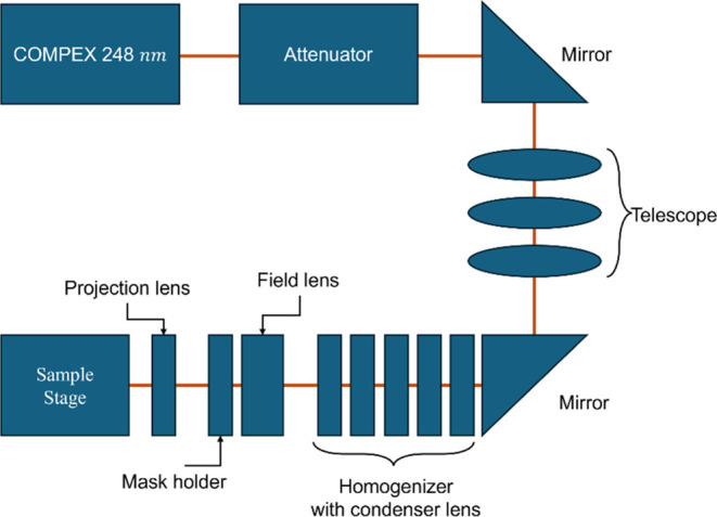
Schematic block diagram outlining the beam delivery system.
Table 2. Various LA Treatment Conditions Used to Prepare a Total of 20 Samplesa.
| Si sample |
Si72Ge28 sample |
||
|---|---|---|---|
| laser energy [mJ] | number of pulses | laser energy [mJ] | number of pulses |
| 20 | 1, 100, 500 | 20 | 1, 100, 500 |
| 30 | 1, 50, 100 | 30 | 1, 100, 500 |
| 40 | 1 | 40 | 1, 100, 500 |
| 50 | 1 | 50 | 1 |
| 60 | 1 | 60 | 1 |
These involve varying both the laser energy and number of pulses.
The selected treatments consider the melting temperatures and layer thickness of both a-Si and a-Si72Ge28. It has been reported that the higher the Ge content in the SiGe alloy, the lower the melting point and the transition temperature between amorphous and crystalline forms.24 For thinner Si layers, increasing the laser energy or the number of pulses may result in material ablation and damage, hence, lower LA treatments are selected to minimize mechanical damage to the samples. This damage has been observed, in previous work, in patterned test structures, and is attributed to the high tensile stress and high strain gradient caused by the steep thermal variation across the film thickness post laser treatment.23
Characterization Techniques
The fabricated layers are characterized pre and post the laser annealing process. The layer thickness is only confirmed visually, pre laser treatment, as a similar deposition recipe is used in prior work.23 In this section, we focus on the initial characterization performed to confirm the transformation of the layer from amorphous to polycrystalline form, which includes an expected increase in surface roughness and decrease in sheet resistivity.
Sheet resistivity, ρS, measurements (Table 3) are performed on blanket layers using a Signatone semiautomatic four-point probe with a Keithley 2400 series source meter and a computerized measurement system. The measured sheet resistance values, RS, and total material thickness, tf, are later used to mathematically calculate ρS using the equation ρS = RStf.23 It must be noted that for the laser annealed layers, this may only be considered as an averaged representation, as variations in the grain microstructure with depth are an expected outcome of laser annealing.18
Table 3. Sheet Resistivity Measurements for the Blanket Si and Si72Ge28 Layers Annealed with Varying Laser Energies and Number of Pulses.
| Si sample |
Si72Ge28 sample |
||||
|---|---|---|---|---|---|
| laser energy [mJ] | pulses | ρS [Ω·cm] | laser energy [mJ] | pulses | ρS [Ω·cm] |
| 30 | 1 | 2.58 | 20 | 1 | 1.14 × 10⁴ |
| 40 | 1 | 1.02 × 10⁻¹ | 30 | 1 | 6.60 × 10² |
| 50 | 1 | 3.36 × 10⁻² | 40 | 1 | 61.2 |
| 30 | 100 | 3.45 × 10⁻² | 50 | 1 | 15.2 |
| 60 | 1 | 2.30 | |||
| 20 | 100 | 2.27 × 10² | |||
| 30 | 100 | 3.59 | |||
The topography of all layers is inspected using a scanning electron microscope (SEM). High resolution top-view images are collected using a Carl Zeiss LEO SUPRA 55 SEM. Images are used to investigate visually the surface roughness of the layers post the laser treatment, while cross-sectional images provide information regarding the overall layer thickness.
The roughness of these wafers is evaluated using stylus profilometry performed on a Veeco Dektak profilometer. Electromechanical measurements involve moving the sample beneath a diamond-tipped stylus that traverses the sample surface. The scan traces consistently start from the amorphous area of the substrate and extend to the surface of the laser treated layer. An average step height is subsequently determined using the interfaced software to estimate the roughness.
Surface-Enhanced Raman Spectroscopy spectra are gathered for all samples at room temperature using a portable i-Raman plus spectrometer (B&W TEK Inc.). The spectrometer is equipped with a 785 nm laser with an output power of 400 mW. During data collection, the laser power is adjusted to 300 mW to optimize the experimental conditions, and an exposure time of 5 min is employed to guarantee a sufficient signal-to-noise ratio and accurate spectral information. Measurements are conducted by randomly collecting spectra from 10 distinct spots for each set of sampling locations. The acquisition of spectral data is carried out using BWSpec software, operating in the Raman shift range of 62–3202 cm–1. This software allows the capture of a background signal (dark) before data acquisition, to be used as reference.
Transmission spectra are collected for all samples using an ultraviolet–visible–infrared (UV–vis-IR) PerkinElmer Lambda 1050+ spectrophotometer, with an integrated sphere setup. Scans are performed in the range from 250 to 2500 nm with a scan speed of 548 nm/min. The beam size is manually adjusted to approximately a 0.25 cm diameter and aligned at the center of the 0.48 × 0.48 cm2 laser treated portion of the surface.
Finally, the thermoelectric measurements are carried out on square-shaped samples measuring 13 × 0.5 mm2 to evaluate the Seebeck coefficient. The experiment is conducted within the temperature range of 400–800 K, using the ULVAC ZEM-3 apparatus. The setup consists in vertically placing the sample on a thin film sample holder which is then placed between an upper and lower electrode inside a heating furnace. The thermal gradient is created by the lower electrode heater. To determine the Seebeck coefficient, upper and lower temperatures and the difference of voltage are measured using thermocouples pressed against the sample’s surface.
Results and Discussion
Surface Roughness and Sample Crystallinity
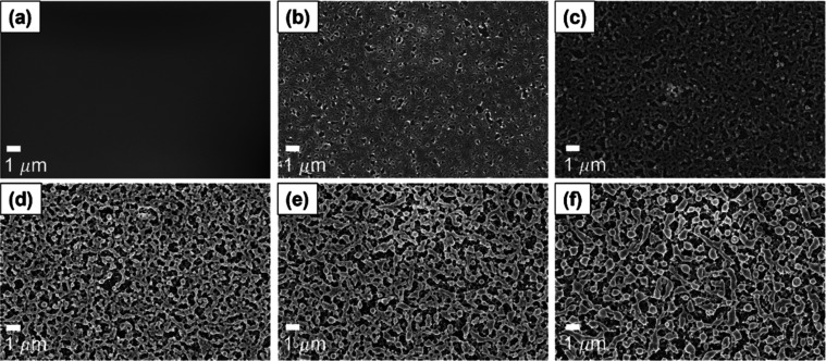
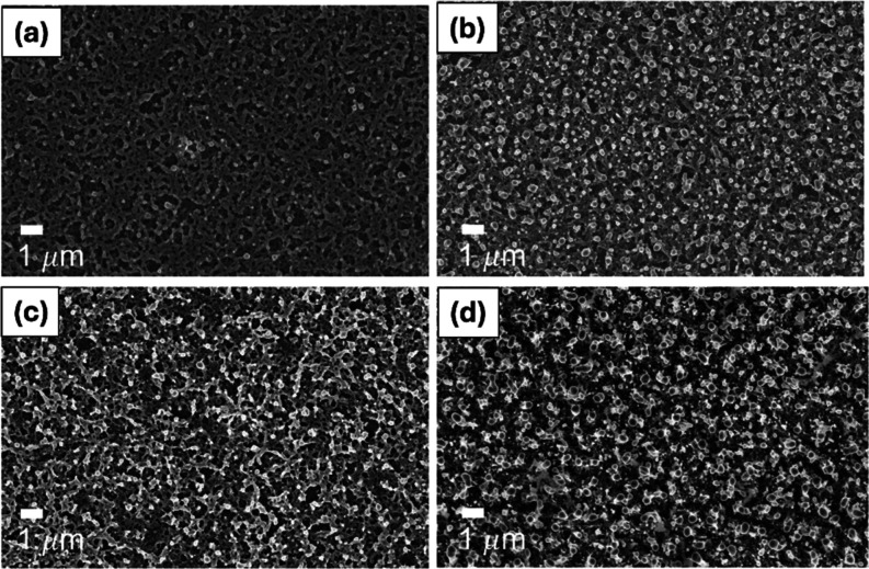
Post laser treatment, the samples are visually observed for surface variations in comparison to the amorphous layer. Figure 2 highlights the surface structure of both pre and post single pulse laser treatments for the 0.366 μm Si layers. The images are used as an initial assessment for the mechanical structure of the layers and to visually confirm the expected increase in surface roughness for increasing single pulse laser energy. Additionally, we also expect a similar increase in surface roughness for an increasing number of pulses of fixed laser energy. Figure 3a,b offers a visual comparison between a Si sample treated with a single 30 mJ pulse and one treated with 100 pulses of the same laser energy, confirming our expectations for increased surface roughness of the latter. The Si72Ge28 sample SEM images (Figure 3c,d) exhibit a similar trend.
Figure 2.
SEM images of (a) pre-laser-treated as-grown amorphous Si and of (b) 20, (c) 30, (d) 40, (e) 50 and (f) 60 mJ single pulse laser treated layers.
Figure 3.
SEM images of the treated Si layer with 30 mJ (a) single pulse and (b) multiple-pulse (100 pulses) and those of the treated Si72Ge28 layer with 30 mJ (c) single pulse and (d) 500 pulses.
While post laser treatments can be used to reduce surface roughness in poly-Si and poly-SiGe layers grown by CVD at 450 °C,32,33 where a gradual increase in laser energy density can decrease the surface roughness, the opposite is expected for the layers presented in this work. Starting with an amorphous layer, it has been shown that an increase in both the laser energy density and the number of pulses causes an increase in the expected crystallization depth and the surface roughness of the sample. The latter may be attributed to the creation of large crystalline structures and voids in these hydrogenated layers when subjected to higher temperatures and longer cooling durations.25
Surface roughness in this work is a desired aspect as long as the material remains intact and is not fully ablated off the substrate layer. As illustrated in our data and discussed in the Introduction section, the nanotexturing of the sample induced by the surface roughness can improve the material’s light trapping and absorption properties. Surface roughness measurements for the laser treated Si and Si72Ge28 layers can be found in Table 4. As the single pulse (SP) laser treatment increases from 30 to 60 mJ, a relative increase by factors of 5.55 and 8.15 is observed for the average surface roughness Ra of both the Si and Si72Ge28 layers, respectively. At a fixed energy value, as the number of laser pulses increases, we observe a further increase in the surface roughness of both the Si and the Si72Ge28 layers. For example, in the case of the Si72Ge28 sample, we observe a relative increase by a factor of 6.64 for the Ra value, if 500 multiple pulses (MP) are used. Similarly, an increase to 100 MP for the Si sample shows a relative increase by a factor of 3.07 for the same parameter.
Table 4. Surface Roughness of Various LA Treatment Conditions of the Si and Si72Ge28 Samplesa.
| Si | ||||
|---|---|---|---|---|
| laser energy [mj] | number of pulses | label | Ra [nm] | Rq [nm] |
| 30 | 1 | 30 mJ/SP | 114.7 | 133.6 |
| 30 | 100 | 30 mJ/100MP | 467.0 | 468.6 |
| 50 | 1 | 50 mJ/SP | 589.1 | 596.2 |
| 60 | 1 | 60 mJ/SP | 751.0 | 829.9 |
| Si72Ge28 | ||||
|---|---|---|---|---|
| laser energy [mJ] | number of pulses | label | Ra [nm] | Rq [nm] |
| 30 | 1 | 30 mJ/SP | 74.2 | 129.0 |
| 30 | 100 | 30 mJ/100MP | 494.7 | 528.8 |
| 30 | 500 | 30 mJ/500MP | 567.0 | 644.2 |
| 40 | 1 | 40 mJ/SP | 299.0 | 323.0 |
| 50 | 1 | 50 mJ/SP | 484.7 | 540.3 |
| 60 | 1 | 60 mJ/SP | 678.7 | 857.2 |
Ra values display the average surface roughness calculated using the height variation between the sample surface peaks and valleys, while Rq represents the root mean square of the height variation between the sample surface peaks and valleys.
While both the SEM images and surface roughness data demonstrate the response of our layers to variations in the laser treatment conditions, the laser-induced transition of the as-grown layers to a polycrystalline form was confirmed initially through sheet resistivity measurements (Table 3) and further validated by Raman spectroscopy (Figures 4 and 5). We note a reduction in the sheet resistivity with an increase in the supplied laser energy. This result is expected when compared to previous work,23 which attributes the outcome to the increase in sample crystallization depth. It is also noted that the treatment conditions for 20 mJ laser energy do not result in sufficient material changes as is further shown in the Raman analysis.
Figure 4.
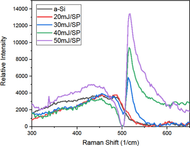
Raman scattering spectra of the as-deposited a-Si layer, and of layers postprocessed using a single pulse (SP) of energy from 20 to 50 mJ.
Figure 5.
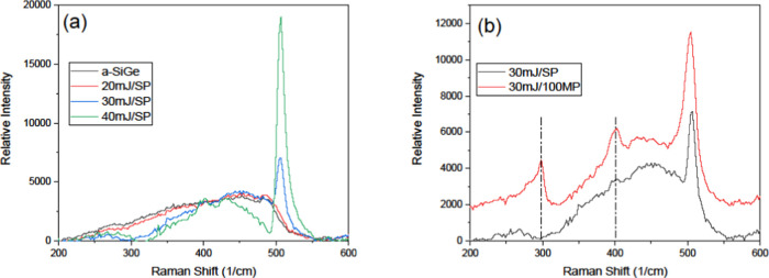
(a) Raman scattering spectra of the as-deposited a-SiGe layer, and of layers postprocessed using a single pulse of energy from 20 to 40 mJ. (b) Raman spectra for a layer processed with a single pulse of 30 mJ and one processed with 100 pulses (MP) of the same energy per pulse, stacked for clarity. The dashed lines indicate the location of Si–Ge and Ge–Ge interactions.
We further investigate the crystallinity of silicon layers using Raman scattering spectra. As shown in Figure 4, in the case of amorphous silicon, a broad Raman band centered at approximately 480 cm–1 is observed. While the sample processed with a 20 mJ pulse shows no significant difference, for the higher energy pulsed samples, a distinct peak emerges, located at 518 cm–1. The effect is associated with the creation of polycrystalline silicon at the surface of the layer. Our observations are in good agreement with the work of Marcins et al.,34 despite their different synthesis process. Moreover, the relative intensity of this peak increases with pulse energy, indicating that a larger part of the material transforms to the polycrystalline state. This increase is accompanied by a decrease in the intensity of the broad amorphous peak centered at 480 cm–1, which can also be attributed to the extended crystallinity of the layer. Nonetheless, the latter remains present for all samples, indicating that the process leads to only partial crystallization. This observation is in line with previous work investigating the influence of laser pulse energy and the number of pulses on the crystallization depth.26 Raman spectra of silicon samples postprocessed with multiple pulses of fixed energy show no significant differences with respect to the single pulse treatment, at the same energy, which can be attributed to the detection limit of the device.
Similarly, the Raman spectra of Si72Ge28 layers are examined under the influence of a single energy pulse ranging from 20 to 40 mJ. Figure 5a depicts the layers, revealing a broad Raman band for both the amorphous layer and the layer treated with a 20 mJ pulse. For increasing energy per pulse, we observe a distinct peak located at 505 cm–1, which corresponds to the Si–Si transverse optical zone edge phonon. These findings are in good agreement with those reported for SiGe layers deposited via low-pressure chemical vapor deposition in previous works.24,25
In contrast to the Si samples, the effect of multiple pulses is significant in the case of Si72Ge28 layers. Specifically, as shown in Figure 5b, layers annealed using multiple 30 mJ pulses exhibit two prominent peaks in the spectral regions of 300 and 400 cm–1, corresponding to Si–Ge and Ge–Ge interactions, respectively, as reported in previous works.35,36 These peaks are absent in the case of a single 30 mJ pulse treatment, suggesting a smaller extent of crystallinity compared to the multiple-pulse case. Similar observations regarding both composition and stress have been documented in previous studies,36−38 further validating our findings. Given that the proportion of Si in our Si72Ge28 layers is much higher than that of Ge, the Si–Si interaction peak is dominant in the spectra, while the Si–Ge and Ge–Ge interactions require a significantly larger extent of crystallinity to be observed.
Thermoelectric Properties
Energy harvesting is feasible via materials that exhibit optimum thermoelectric properties. We evaluate these properties by measuring the temperature-dependent Seebeck coefficient (S) and electrical conductivity (σ) for the fabricated Si and Si72Ge28 nanostructured layers, from which we calculate the power factor (PF = S2σ). Another significant factor for energy conversion assessment of these layers is the material’s thermal conductivity (κ) which is used along with the PF to define the dimensionless figure of merit (zT = S2σT/κ). We note here that characterizing thin film layers presents distinct challenges compared to bulk materials, due to their induced high surface roughness, a result of both their small layer thickness and laser annealing treatment. Further difficulties include establishing reliable electrical contacts and overcoming the limitations imposed by the substrate to both the processing and the measurement temperatures.
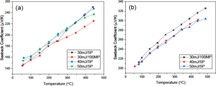
Figure 6a depicts the temperature-dependent behavior of the Seebeck coefficient in nanostructured Si layers annealed with single and multiple pulses. For samples irradiated with pulses of energy below 30 mJ, the high resistivity of the layer did not allow the measurement of the Seebeck coefficient. A slight increase in the Seebeck coefficient is observed with rising temperature, ranging from 150 μV/m at 50 °C to 250 μV/m at 500 °C. Moreover, Figure 6a depicts minimal deviation in the Seebeck coefficient across samples treated with pulses of different energy.
Figure 6.
Temperature-dependent variation of the Seebeck coefficient for (a) single pulsed (SP) and multiple-pulsed (MP) Si layers and for (b) nanostructured Si72Ge28 layers.
Similar results have been observed in earlier studies on heavily doped n/p-type poly-Si materials, indicating a similar magnitude of the Seebeck coefficient within a temperature range of −50–300 °C. The reported Seebeck coefficient values have consistently ranged from 110 to 250 μV/m across these studies.39
In comparison to the Si layers, the Si72Ge28 layers exhibit higher Seebeck coefficient values. The temperature dependency of the Seebeck coefficient for nanostructured Si72Ge28 layers is illustrated in Figure 6b. Similar to silicon layers, samples irradiated with energy inputs lower than 30 mJ fall below the equipment’s detection threshold due to high sheet resistivity values (Table 3). Our measurements pertain to p-type SiGe and demonstrate an increase with temperature. Furthermore, the values exhibit minimal change with varying energy per pulse. For instance, in the sample laser-annealed at 30 mJ with multiple pulses, the Seebeck coefficient increases from 215 μV/K at 100 °C to 320 μV/K at 450 °C. Similarly, layers treated with single pulses of 40 and 50 mJ show only a minor variation with the Seebeck coefficient ranging from 215 μV/K at 100 °C to 300 μV/K at 450 °C.
The observed values are significantly higher than those reported in literature for nanostructured SiGe synthesized through mechanical alloying and annealing approaches. Previous studies report a maximum Seebeck coefficient of approximately 160 μV/K at 900 °C.40 In comparison to other works on laser-annealed SiGe thin films, bulk nanostructured SiGe and other types of SiGe materials, our results correspond to the Seebeck coefficient values of thin films.41−45 The observed increase has been attributed to energy filtering and phonon drag effects.41−43 It is therefore clear that the meticulous selection of laser parameters, including energy, pulse duration, and repetition rate, is paramount to produce nanostructured SiGe layers with higher Seebeck coefficients than bulk nanostructured SiGe.
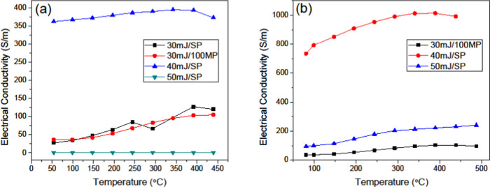
The measured temperature-dependent electrical conductivity of the nanostructured Si and SiGe layers annealed with single and multiple pulses are presented in Figure 7. The data reveal an increase in electrical conductivity with rising temperature, which sharply contrasts with the general behavior observed in bulk materials. This increase in conductivity is attributed to the inhomogeneous, porous and percolated structure of the thin films, challenging the conventional grain boundary trapping model.46 Moreover, the high temperature electrical behavior in these nanocrystalline materials may also be explained by the presence of tunnel junctions between conductive regions or low-conductivity barriers,47,48 making these materials more sensitive to temperature variations compared to their bulk counterparts.
Figure 7.
Temperature-dependent variation of the electrical conductivity for (a) single pulsed and multiple-pulsed Si layers; and for (b) nanostructured Si72Ge28 layers.
Laser treatment energy also plays a critical role in the results of Figure 7. Samples annealed with 50 mJ SP and 30 mJ 100 MP exhibit lower electrical conductivity due to their higher surface roughness, resulting in fewer and narrower conductive paths. In contract, the 40 mJ SP sample displays a higher electrical conductivity due to its more uniform surface morphology, reduced roughness and optimal laser parameters, consistent with prior studies.49
The highest recorded electrical conductivity value of 1010 S/m for the SiGe nanostructured layers demonstrates a significant enhancement and highlights the improved performance of the 40 mJ SP sample. Our findings are substantiated by previous research50 and underscore the critical role of the laser parameters in optimizing electrical performance. Furthermore, the values measured in this study, ranging from 100 to 1010 S/m for temperatures between 100 and 1000 K, align with those reported in the literature for short-pulsed laser sintered nanoparticle thin films.48,50
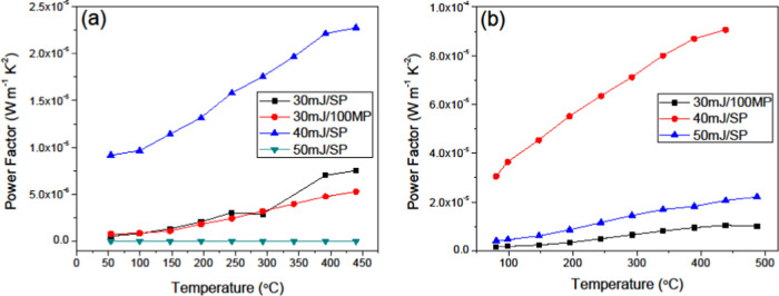
A qualitatively similar relationship between the power factor (Figure 8) and electrical conductivity (Figure 7) of the Si and SiGe layers is observed, suggesting that the enhancement cannot be attributed solely to the Seebeck coefficient values. The PF values for the SiGe layers treated with the optimal single pulse energy of 40 mJ and ranging between 30 and 90 μW/m·K2, are consistent with values reported in the literature. Power factors of Si80Ge20 nanomeshed films51 range from approximately 445 μW/m·K2, for the largest pore diameter of (294 ± 5) nm, to around 65 μW/m·K2, for the smallest pore diameter of (31 ± 4) nm.51 It is also reported that as the pore diameter decreases, the power factor converges toward that of continuous films, approximately 24 μW/m·K2, due to increasing similarity in structure and scattering mechanisms.52
Figure 8.
Temperature-dependent variation of the power factor for (a) single pulsed and multiple-pulsed Si layers; and for (b) nanostructured Si72Ge28 layers.
Measuring thermal conductivity in layers exhibiting significant roughness, high porosity and irregular surface structure can be very challenging. Time-domain, thermo-reflectance measurements are, in this case, dominated by high intensity, scattered signals that result in a low signal-to-noise ratio. Consequently, this limits our ability to model the thermal properties more effectively, impacting the overall assessment of the thermoelectric performance of the materials under investigation.
For the current study, the figure of merit (zT) for these nanostructured layers can be estimated using thermal conductivity data available in the literature. For instance, the best SiGe sample, produced by single pulse laser annealing at 40 mJ, exhibits a Seebeck coefficient of 300 μV/K at 450 °C, an electrical conductivity of 992 S/m at the same temperature, and a thermal conductivity of 1.37 W/m·K at 600 °C.53 Using these parameters, the figure of merit at 450 °C is estimated to be 0.04.
While the Seebeck coefficient remains relatively high and stable compared to the existing literature, the highest zT achieved in this study is less than 0.1 at room temperature. This limitation arises primarily from the low thermoelectric power factor of our samples and is attributed to their reduced electrical conductivity and the constraint in measuring thermal conductivity.
Prior studies have extensively investigated nanostructures such as nanowires, porous nanomeshes, and nanocrystalline bulk materials, elucidating their thermoelectric properties.54 However, these studies have emphasized that optimizing the thermoelectric properties of nanostructured layers inevitably affects thermal conductivity. It has been indicated that achieving a phonon mean free path exceeding both the grain size and the electron mean free path is crucial. Therefore, further studies should focus on comprehensive thermal conductivity assessments to advance our understanding of nanostructured silicon’s thermoelectric performance.55,56
Future work must focus on carefully adjusting the laser energy, pulse count and potentially incorporating doping strategies to enhance the thermoelectric performance of such nanostructured layers and achieve a higher figure of merit. While this study does not focus on optimizing electrical conductivity, the enhancement of thermoelectric performance arises from the fact that initially amorphous Si and SiGe layers can demonstrate promising thermoelectric performance by means of a single pulse laser surface treatment. We continue to show, that in addition to improved thermoelectric performance, the same treatment can enhance the material’s optical absorption, thereby enabling hybrid energy harvesting capabilities.
Optical Properties of Nanostructured Si and Si72Ge28
UV–vis-IR transmission spectra of the a-Si sample, as well as for the samples annealed using a single pulse with energies ranging from 20 to 60 mJ, are shown in Figure 9. The untreated sample exhibits the characteristic spectrum observed in previous works.57−59 Spectra above 2000 nm are not presented due to low signal-to-noise ratio with respect to the reference. The sample treated with a 20 mJ pulse does not exhibit a significant difference in its transmission characteristics with respect to the untreated sample. For pulse energy of 30 mJ and above we are able to observe a clear trend of diminishing transmittance with increasing single pulse energy. A reduction in intensity of the transmission peaks at higher wavelength values is observed as the laser energy is increased. This effect may be attributed to the higher crystallinity resulting from the increased deposited laser energy, as confirmed from the Raman observations. For crystalline silicon (c-Si) compared to a-Si, higher absorption at longer wavelengths is expected.60 Hence, we deduce that the increased crystallinity after treatment contributed to the reduced intensity in transmission (higher absorption) at longer wavelengths.
Figure 9.
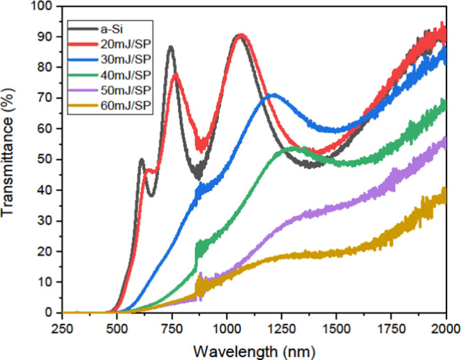
Transmittance of a-Si layer in comparison to variations in single pulse (SP) laser energy treatments from 20 to 60 mJ.
In addition to the reduction in transmission peak intensity, we also observe a red-shift in transmittance spectra, which corresponds to an expected blue-shift in absorption. An increase in the mean size of nanocrystalline Si can lead to a red-shift in emission/absorption spectra.61,62 Extending these observations, a reduced mean size of nanocrystalline Si should lead to a red-shift in transmission spectra. In our samples, a reduction in nanocrystalline Si size corresponds to an increase in surface nanostructuring. As seen from our surface roughness and SEM data, higher laser energy treatment induces more surface nanostructuring, which can explain the observed red-shift in the transmission spectra. Complementary reflectance measurements, not shown here for brevity, exhibit the same spectral behavior.
The absorbance is here calculated via the Beer–Lambert Law formula
and presented in Figure 10, in agreement with previous work.63,64 Enhanced absorbance is observed for the samples treated with a single pulse of 30 mJ of energy and above. It is clear that a single pulse of 20 mJ is not sufficient to induce significant changes in the amorphous sample, as confirmed by Raman observations. This effect is better depicted in Figure 11, where the enhancement factor, defined as the ratio of the energy absorbed by the treated samples with respect to the untreated a-Si, is presented as a function of wavelength.65 The treated samples can reach enhancement absorption factors up to 25 times compared to the untreated samples in the wavelength range of 630–1200 nm with an optimal single pulse laser treatment of 60 mJ.
Figure 10.
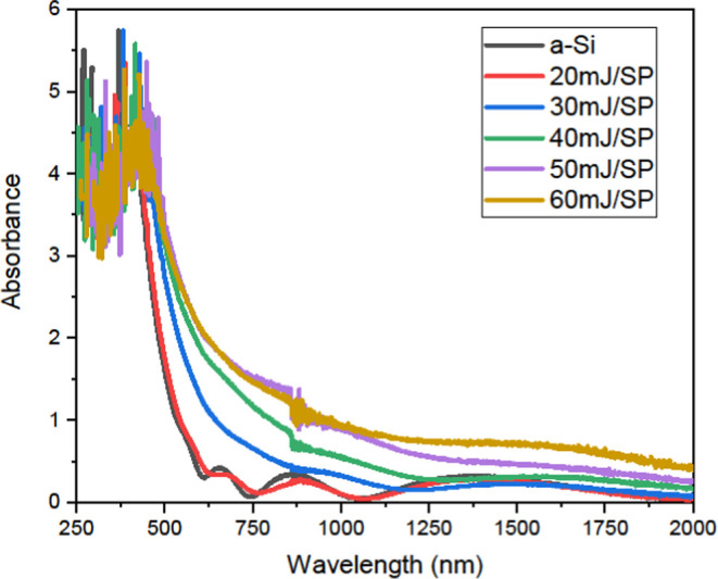
Calculated absorbance of a-Si layer in comparison to variations in single pulse (SP) laser energy treatments from 20 to 60 mJ.
Figure 11.
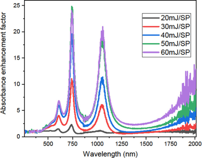
Calculated absorbance enhancement factor of the treated samples in comparison to the as-grown a-Si layer.
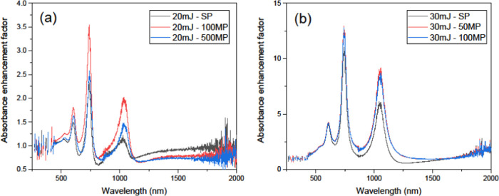
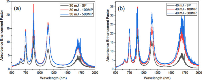
The transmittance of samples treated with multiple pulses of a particular energy is also measured to investigate the effect of multiple-pulse annealing (Figure 12). Our results show that samples treated with 100 and 500 pulses of 20 mJ energy and a pulse rate of 10 Hz, respectively, show very little change in absorbance enhancement factor compared to the single pulse case. This suggests that the energy deposited per pulse is not enough to produce significant structural alteration of the sample surface (Figure 12a).
Figure 12.
Calculated absorbance enhancement factor of the single pulse and multiple-pulse treated Si in comparison to the as-grown a-Si layer with (a) 20 and (b) 30 mJ, respectively.
Furthermore, samples irradiated with 50 and 100 pulses, respectively, of 30 mJ energy exhibit only a limited improvement, with respect to the absorbance enhancement factor, while the latter appears saturated for the number of pulses here considered (Figure 12b).
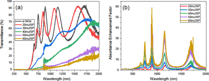
In the case of SiGe samples treated with a single pulse of increasing energy, the spectral characteristics in transmission are similar to the Si case, albeit significantly pronounced, as shown in Figure 13a. Furthermore, our results clearly show very high enhancement factors for samples treated with single pulses of energy up to 60 mJ, with no sign of saturation for the used annealing energy (Figure 13b). In the future, pulses of even higher energy could be used to determine the saturation level of the optical enhancement factor of the Si72Ge28 samples.
Figure 13.
(a) Transmittance of Si72Ge28 layers treated with a single pulse of energy ranging from 20 to 60 mJ. (b) Calculated absorbance enhancement factor of the single pulse treated samples in comparison to the as-grown a-Si72Ge28 layer for laser treatments from 20 to 60 mJ, respectively.
We observe that the enhancement factors increase steadily, reaching a maximum of 60 times in the range of 880 nm for the 60 mJ laser treatment. The increased surface roughness and porosity facilitate light absorption by increasing the effective surface area and enhancing light-matter interactions. However, this increased roughness and porosity do not similarly benefit electrical conductivity, resulting in only a 22-fold improvement in optical absorption at the optimal thermoelectric treatment of 40 mJ SP. This nuanced understanding underscores the need for precise optimization based on specific desired properties in the application of such laser treatments.
In the case of multiple-pulse treatments of Si72Ge28 (Figure 14), we observe an improved enhancement factor with increasing energy and number of pulses. The analysis strongly indicates a very efficient surface alteration of the samples, as confirmed from the visual SEM and surface profiler roughness measurements. This alteration results in a significant increase in the absorbance of the irradiated power for several regions of the considered spectra. Comparing samples irradiated with 100 and 500 pulses at energies of 30 and 40 mJ, respectively, we observe a substantial improvement in absorbance. However, saturation with an increasing number of pulses is also evident (Figures 13 and 14a,b).
Figure 14.
Calculated absorbance enhancement factor of the single pulse and multiple-pulse treated Si72Ge28 in comparison to the as-grown a-Si72Ge28 layer with (a) 30 and (b) 40 mJ respectively.
Conclusions
Surface nanostructuring of as-grown a-Si and a-Si72Ge28 layers is successfully achieved using a KrF excimer laser, leading to the formation of polycrystalline layers with enhanced optical absorption and promising thermoelectric properties. By carefully tuning the laser energy and pulse count, we observe an increase in surface roughness and nanostructuring, which directly contribute to the improved performance of the treated samples. While, a single pulse of 60 mJ applied to poly-Si72Ge28 results in a remarkable 60-fold enhancement in optical absorption at 880 nm, when examining both the thermoelectric and optical properties, we find that 40 mJ produces a layer with both promising thermoelectric properties, featuring a power factor of 90 μW/m·K2 at 450°C, and an optical enhancement factor of 22-fold. These results underscore the potential of laser treated poly-Si72Ge28 as a with hybrid energy harvesting capabilities. Furthermore, the laser treatment offers a broader range of suitable applications by significantly reducing the processing time and temperature budget compared to traditional nanostructuring techniques.
Methods
Nanostructured Layer Fabrication
Amorphous Si and Si72Ge28 layers are deposited at 210 °C directly on Corning Eagle XG glass substrates using an Oxford Plasma Lab 100 plasma enhanced chemical vapor deposition tool. Both layers are postprocessed with a laser annealing treatment conducted using a lambda physik compex 205 KrF excimer laser with a fixed output of 248 nm and 24 ns pulse duration. Both single pulse and multiple-pulse laser treatments were employed to induce variations in the surface nanostructuring of the Si and the Si72Ge28 layers.
Characterization
Initial characterization of the layers is performed using a Signatone semiautomatic four-point probe with a Keithley 2400 series source meter and a computerized measurement system, to confirm the reduction in the layers’ sheet resistivity due to laser induced crystallization.
The topography of all layers is inspected using a high-resolution Carl Zeiss LEO SUPRA 55 SEM to visually confirm the surface nanostructuring. This is followed by quantitative surface roughness measurements using a Veeco Dektak profilometer.
Layers showing promising sheet resistivity measurements are further examined to acquire their Raman spectra using a portable i-Raman plus spectrometer (B&W TEK) with a 785 nm laser and an output power of 400 mW.
Transmission spectra are collected for both the Si and Si72Ge28 layers using a UV–vis-IR PerkinElmer Lambda 1050+ spectrophotometer. The beam size is manually adjusted to approximately a 0.25 cm diameter and aligned to the center of the nanostructured layer and transmission scans in the range from 250 to 2500 nm are collected.
The thermoelectric performance is completed using a ULVAC ZEM-3 apparatus. The samples are resized to 13 × 0.5 mm2 and measurements are conducted within the temperature range of 400–800 K.
Acknowledgments
The authors would like to acknowledge A. Moghnieh, Université du Littoral Côte d’Opale, Dunkirk, France; and A. Nour and A. El Beltagy, Youssef Jameel Science and Technology Research Center, American University in Cairo, Cairo, Egypt, for their significant technical contributions.
Glossary
Abbreviations
- PECVD
plasma enhanced chemical vapor deposition
- a-Si
amorphous silicon
- a-SiGe
amorphous silicon germanium
- poly-Si
polycrystalline silicon
- poly-SiGe
polycrystalline silicon germanium
- c-Si
crystalline silicon
- SP
single pulse
- MP
multiple pulses
- LA
laser annealing
- RF
radio frequency
- IMDs
implantable medical devices
Author Contributions
J.E.R., E.B. and S.C. wrote the main manuscript text and analyzed relevant data. Samples fabricated by J.E.R. Sample sheet resistivity, optical and SEM measurements conducted by J.E.R. Raman spectroscopy and surface roughness measurements conducted by E.B. Thermoelectric measurements conducted by F.G. All authors have reviewed the manuscript and given approval to the final version.
This research was supported by the Sorbonne University Abu Dhabi (SUAD) research funding.
The authors declare no competing financial interest.
References
- Zimmermann S.; Helmers H.; Tiwari M. K.; Paredes S.; Michel B.; Wiesenfarth M.; Bett A. W.; Poulikakos D. A High-Efficiency Hybrid High-Concentration Photovoltaic System. Int. J. Heat Mass Transfer 2015, 89, 514–521. 10.1016/j.ijheatmasstransfer.2015.04.068. [DOI] [Google Scholar]
- Sundarraj P.; Maity D.; Royb S. S.; Taylor R. A. Recent Advances in Thermoelectric Materials and Solar Thermoelectric Generators – A Critical Review. RSC Adv. 2014, 4, 46860–46874. 10.1039/C4RA05322B. [DOI] [Google Scholar]
- Özcan Y.; Daniz E. Solar Thermal Waste Heat Energy Recovery in Solar Distillation Systems by Using Thermoelectric Generators. Eng. Sci. Technol. Int. J. 2023, 40, 101362 10.1016/j.jestch.2023.101362. [DOI] [Google Scholar]
- Farret F. A.; Vieira E. A.. Recovery of Photovoltaic Module Heat Using Thermoelectric Effect. In Renewable Energy - Resources, Challenges and Applications; Al Qubeissi M.; El-kharouf A.; Soyhan H. S., Eds.; IntechOpen, 2020. [Google Scholar]
- Shaukat H.; Ali A.; Ali S.; Altabey W. A.; Noori M.; Kouritem S. A. Applications of Sustainable Hybrid Energy Harvesting: A Review. J. Low Power Electron. Appl. 2023, 13, 62 10.3390/jlpea13040062. [DOI] [Google Scholar]
- Gołąbek J.; Strankowski M. A Review of Recent Advances in Human-Motion Energy Harvesting Nanogenerators, Self-Powering Smart Sensors and Self-Charging Electronics. Sensors 2024, 24, 1069 10.3390/s24041069. [DOI] [PMC free article] [PubMed] [Google Scholar]
- Sohail A.; Ali A.; Shaukat H.; Bhatti F. M.; Ali S.; Kouritem S. A.; Noori M.; Altabey W. A. Integrating Self-Powered Medical Devices with Advanced Energy Harvesting: A Review. Energy Strategy Rev. 2024, 52, 101328 10.1016/j.esr.2024.101328. [DOI] [Google Scholar]
- Xu C.; Song Y.; Han M.; Zhang H. Portable and Wearable Self-Powered Systems Based on Emerging Energy Harvesting Technology. Microsyst. Nanoeng. 2021, 7, 25 10.1038/s41378-021-00248-z. [DOI] [PMC free article] [PubMed] [Google Scholar]
- Dipon W.; Gamboa B.; Estrada M.; Flynn W. P.; Guo R.; Bhalla A. Self-Sustainable IoT-Based Remote Sensing Powered by Energy Harvesting Using Stacked Piezoelectric Transducer and Thermoelectric Generator. Micromachines 2023, 14, 1428 10.3390/mi14071428. [DOI] [PMC free article] [PubMed] [Google Scholar]
- Abdin Z.; Alim M. A.; Saidur R.; Islam M. R.; Rashmi W.; Mekhilef S.; Wadi A. Solar Energy Harvesting with the Application of Nanotechnology. Renewable Sustainable Energy Rev. 2013, 26, 837–852. 10.1016/j.rser.2013.06.023. [DOI] [Google Scholar]
- Joshi G.; Lee H.; Lan Y.; Wang X.; Zhu G.; Wang D.; Gould R. W.; Cuff D. C.; Tang M. Y.; Dresselhaus M. S.; Chen G.; Ren Z. Enhanced Thermoelectric Figure-of-Merit in Nanostructured p-type Silicon Germanium Bulk Alloys. Nano Lett. 2008, 8, 4670–4674. 10.1021/nl8026795. [DOI] [PubMed] [Google Scholar]
- Dong H.; Wen B.; Melnik R. Relative importance of grain boundaries and size effects in thermal conductivity of nanocrystalline materials. Sci. Rep. 2014, 4, 7037 10.1038/srep07037. [DOI] [PMC free article] [PubMed] [Google Scholar]
- Rowe D. M.Miniature Semiconductor Thermoelectric Devices. In Handbook of Thermoelectrics, 1st ed.; CRC Press: Boca Raton, 2017; p 18. [Google Scholar]
- McNaughton A. G.Commercially Available Generators. In Handbook of Thermoelectrics, 1st ed.; Rowe D. M., Ed.; CRC Press: Boca Raton, 2017; p 12. [Google Scholar]
- Ahmad S.; Singh A.; Bohra A.; Basu R.; Bhattacharya S.; Bhatt R.; Meshram K. N.; Roy M.; Sarkar S. K.; Hayakawa Y.; Debnath A. K.; Aswal D. K.; Gupta S. K. Boosting thermoelectric performance of p-type SiGe alloys through in-situ metallic YSi2 nanoinclusions. Nano Energy 2016, 27, 282–297. 10.1016/j.nanoen.2016.07.002. [DOI] [Google Scholar]
- Basu R.; Singh A. High temperature Si-Ge alloy towards thermoelectric applications: A comprehensive review. Mater. Today Phys. 2021, 21, 100468 10.1016/j.mtphys.2021.100468. [DOI] [Google Scholar]
- Basu R.; Bhattacharya S.; Bhatt R.; Roy M.; Ahmad S.; Singh A.; Navaneethan M.; Hayakawa Y.; Aswal D. K.; Gupta S. K. Improved thermoelectric performance of hot pressed nanostructured n-type SiGe bulk alloys. J. Mater. Chem. A 2014, 2, 6922–6930. 10.1039/c3ta14259k. [DOI] [Google Scholar]
- Bathula S.; Jayasimhadri M.; Gahtori B.; Singh N. K.; Tyagi K.; Srivastava A. K.; Dhar A. The role of nanoscale defect features in enhancing the thermoelectric performance of p-type nanostructured SiGe alloys. Nanoscale 2015, 7, 12474–12483. 10.1039/C5NR01786F. [DOI] [PubMed] [Google Scholar]
- Rowe D. J.; Kortshagen U. R. Boron- and phosphorus-doped silicon germanium alloy nanocrystalsdnon thermal plasma synthesis and gasphase thin film deposition. APL Mater. 2014, 2, 022104 10.1063/1.4865158. [DOI] [Google Scholar]
- Ascencio-Hurtado C. R.; Torres A.; Ambrosio R.; Moreno M.; Álvarez-Quintana J.; Hurtado-Macías A. N-type amorphous silicon-germanium thin films with embedded nanocrystals as a novel thermoelectric material of elevated zT. J. Alloys Compd. 2022, 890, 161843 10.1016/j.jallcom.2021.161843. [DOI] [Google Scholar]
- Singh S.; Hirata K.; Pandey S. K.; Takeuchi T.. Recent Advances in Energy Harvesting from Waste Heat Using Emergent Thermoelectric Materials. In Emerging Materials Design, Characterization and Applications; Thoutam L. R.; Tayal S.; Ajayan J., Eds.; Springer Nature, 2021. [Google Scholar]
- Singh S.; Poudel B.; Nozariasbmarz A.; Takeuchi T.; Priya S.. Constructive Approach Towards Design of High-Performance Thermoelectrics, Thermal Diodes, and Thermomagnetic Devices for Energy Generation Applications. In Energy Harvesting and Storage Devices, Sustainable Materials and Methods, 1st ed.; CRC Press, 2023; p 28. [Google Scholar]
- El-Rifai J.; Sedky S.; Hoof R. V.; Severi S.; Lin D.; Sangameswaran S.; Puers R.; Hoof C. V.; Witvrouw A. SiGe MEMS at Processing Temperatures Below 250 °C. Sens. Actuators, A 2012, 188, 230–239. 10.1016/j.sna.2012.01.035. [DOI] [Google Scholar]
- Sedky S. SiGe: An Attractive Material for Post-CMOS Processing of MEMS. Microelectron. Eng. 2007, 84, 2491–2500. 10.1016/j.mee.2007.05.055. [DOI] [Google Scholar]
- Sedky S.; Bayoumy A.; Alaa A.; Nagy A.; Witvrouw A. Optimal Conditions for Micromachining Si1–xGex at 210 °C. J. Microelectromech. Syst. 2007, 16, 581–588. 10.1109/JMEMS.2007.896703. [DOI] [Google Scholar]
- Sedky S.; Gromova M.; Van der Donck T.; Celis J.–P.; Witvrouw A. Characterization of KrF Excimer Laser Annealed PECVD SixGe1-x for MEMS Post-Processing. Sens. Actuators, A 2006, 127, 316–323. 10.1016/j.sna.2006.01.035. [DOI] [Google Scholar]
- Lindorf M.; Rohrmann H.; Katona G. L.; Beke D. L.; Pernau H.-F.; Albrecht M. Nanostructured SiGe Thin Films Obtained Through MIC Processing. Mater. Today: Proc. 2015, 2, 557–565. 10.1016/j.matpr.2015.05.076. [DOI] [Google Scholar]
- Nozariasbmarz A.; Roy P.; Zamanipour Z.; Dycus J. H.; Cabral M. J.; LeBeau J. M.; Krasinski J. S.; Vashaee D. Comparison of Thermoelectric Properties of Nanostructured Mg2Si, FeSi2, SiGe, and Nanocomposites of SiGe–Mg2Si, SiGe–FeSi2. APL Mater. 2016, 4, 104814 10.1063/1.4966138. [DOI] [Google Scholar]
- Martín-Palma R. J.; McAtee P. D.; Ramadan R.; Lakhtakia A. Hybrid Nanostructured Porous Silicon-Silver Layers for Wideband Optical Absorption. Sci. Rep. 2019, 9, 7291 10.1038/s41598-019-43712-7. [DOI] [PMC free article] [PubMed] [Google Scholar]
- Magdi S.; El-Rifai J.; Swillam M. A. One Step Fabrication of Silicon Nanocones with Wide-Angle Enhanced Light Absorption. Sci. Rep. 2018, 8, 4001 10.1038/s41598-018-22100-7. [DOI] [PMC free article] [PubMed] [Google Scholar]
- Magdi S.; El Rifai J.; Swillam M. Litho-Free Fabrication of Crystalline Silicon Nanowires Using Amorphous Silicon Substrate for Wide-Angle Energy Absorption Applications. ACS Appl. Nano Mater. 2018, 1, 2990–2996. 10.1021/acsanm.8b00598. [DOI] [Google Scholar]
- Chen Y.-C.; Lin J.-X.; Chen C.-L.. Method for Planarizing Polysilicon. U.S. Patent US2004/0055999A1, 2003.
- Gonzalez P.; Haspeslagh L.; Severi S.; De Meyer K.; Witvrouw A. In Piezoresistivity and Electrical Properties of Poly-SiGe, 2010 Proceedings of the European Solid State Device Research Conference; IEEE: Seville, Spain, 2010; pp 476–479.
- Marcins G.; Butikova J.; Tale I.; Polyakov B.; Kalendarjov R.; Muhin A. Crystallization Processes of Amorphous Si by Thermal Annealing and Pulsed Laser Processing. IOP Conf. Ser.: Mater. Sci. Eng. 2011, 23, 012035 10.1088/1757-899X/23/1/012035. [DOI] [Google Scholar]
- Alonso M. I.; Winer K. Raman Spectra of c-Si1-xGex Alloys. Phys. Rev. B 1989, 39, 10056 10.1103/PhysRevB.39.10056. [DOI] [PubMed] [Google Scholar]
- Olivares J.; Martin P.; Rodriguez A.; Sangrador J.; Jiménez J.; Rodriguez T. Raman Spectroscopy Study of Amorphous SiGe Films Deposited by Low Pressure Chemical Vapor Deposition and Polycrystalline SiGe Films Obtained by Solid-Phase Crystallization. Thin Solid Films 2000, 358, 56–61. 10.1016/S0040-6090(99)00711-7. [DOI] [Google Scholar]
- Tsang J. C.; Mooney P. M.; Dacol F.; Chu J. O. Measurements of Alloy Composition and Strain in Thin GexSi1-x Layers. J. Appl. Phys. 1994, 75, 8098–8108. 10.1063/1.356554. [DOI] [Google Scholar]
- Brya W. J. Raman Scattering in Ge Si Alloys. Solid State Commun. 1973, 12, 253–257. 10.1016/0038-1098(73)90692-3. [DOI] [Google Scholar]
- Zhou H.; Kropelnicki P.; Tsai J. M.; Lee C. Study of the Thermoelectric Properties of Heavily Doped Poly-Si in High Temperature. Procedia Eng. 2014, 94, 18–24. 10.1016/j.proeng.2013.10.011. [DOI] [Google Scholar]
- Tayebi L.; Zamanipour Z.; Mozafari M.; Norouzzadeh P.; Krasinski J. S.; Ede K. F.; Vashaee D.. Differential Thermal Analysis of Nanostructured Si0.80Ge0.20 Thermoelectric Material2012 IEEE Green Technologies Conference; IEEE: Tulsa, 2012; pp 1–4.
- Xie K.; Mork K.; Kortshagen U.; Gupta M. C. High Temperature Thermoelectric Properties of Laser Sintered Thin Films of Phosphorous-Doped Silicon-Germanium Nanoparticles. AIP Adv. 2019, 9, 015227 10.1063/1.5085016. [DOI] [Google Scholar]
- Stoib B.; Langmann T.; Matich S.; Antesberger T.; Stein N.; Angst S.; Petermann N.; Schmechel R.; Schierning G.; Wolf D. E.; Wiggers H.; Stutzmann M.; Brandt M. S. Laser-Sintered Thin Films of Doped SiGe Nanoparticles. Appl. Phys. Lett. 2012, 100, 231907 10.1063/1.4726041. [DOI] [Google Scholar]
- Wang X. W.; Lee H.; Lan Y. C.; Zhu G. H.; Joshi G.; Wang D. Z.; Yang J.; Muto A. J.; Tang M. Y.; Klatsky J.; Song S.; Dresselhaus M. S.; Chen G.; Ren Z. F. Enhanced Thermoelectric Figure of Merit in Nanostructured N-Type Silicon Germanium Bulk Alloy. Appl. Phys. Lett. 2008, 93, 193121 10.1063/1.3027060. [DOI] [PubMed] [Google Scholar]
- Lee H.; Vashaee D.; Wang D. Z.; Dresselhaus M. S.; Ren Z. F.; Chen G. Effects of Nanoscale Porosity on Thermoelectric Properties of SiGe. J. Appl. Phys. 2010, 107, 094308 10.1063/1.3388076. [DOI] [Google Scholar]
- Valalaki K.; Benech P.; Nassiopoulou A. G. High Seebeck Coefficient of Porous Silicon: Study of the Porosity Dependence. Nanoscale Res. Lett. 2016, 11, 201 10.1186/s11671-016-1411-z. [DOI] [PMC free article] [PubMed] [Google Scholar]
- Seto J. Y. W. The Electrical Properties of Polycrystalline Silicon Films. J. Appl. Phys. 1975, 46, 5247–5254. 10.1063/1.321593. [DOI] [Google Scholar]
- Hu G. Y.; O’Connell R. F.; He Y. L.; Yu M. B. Electronic Conductivity of Hydrogenated Nanocrystalline Silicon Films. J. Appl. Phys. 1995, 78, 3945–3948. 10.1063/1.359914. [DOI] [Google Scholar]
- Sinkkonen J. DC Conductivity of a Random Barrier Network. Phys. Status Solidi B 1980, 102, 621–627. 10.1002/pssb.2221020222. [DOI] [Google Scholar]
- Xie K.; Mork K.; Held J. T.; Mkhoyan K. A.; Kortshagen U.; Gupta M. C. Quasi Continuous Wave Laser Sintering of Si-Ge Nanoparticles for Thermoelectrics. J. Appl. Phys. 2018, 123, 094301 10.1063/1.5018337. [DOI] [Google Scholar]
- Stoib B.; Langmann T.; Matich S.; Antesberger T.; Stein N.; Angst S.; Petermann N.; Schmechel R.; Schierning G.; Wolf D. E.; Wiggers H.; Stutzmann M.; Brandt M. S. Laser-Sintered Thin Films of Doped SiGe Nanoparticles. Appl. Phys. Lett. 2012, 100, 231907 10.1063/1.4726041. [DOI] [Google Scholar]
- Perez-Taborda J. A.; Muñoz Rojo M.; Maiz J.; Neophytou N.; Matrin-Gonzalez M. Ultra-Low Thermal Conductivities in Large-Area Si-Ge Nanomeshes for Thermoelectric Applications. Sci. Rep. 2016, 6, 32778 10.1038/srep32778. [DOI] [PMC free article] [PubMed] [Google Scholar]
- Taborda J. A. P.; Romero J. J.; Abad B.; Muñoz-Rojo M.; Mello A.; Briones F.; Gonzalez M. S. Low Thermal Conductivity and Improved Thermoelectric Performance of Nanocrystalline Silicon Germanium Films by Sputtering. Nanotechnology 2016, 27, 175401 10.1088/0957-4484/27/17/175401. [DOI] [PubMed] [Google Scholar]
- Wang X. W.; Lee H.; Lan Y. C.; Zhu G. H.; Joshi G.; Wang D. Z.; Yang J.; Muto A. J.; Tang M. Y.; Klatsky J.; Song S.; Dresselhaus M. S.; Chen G.; Ren Z. F. Enhanced Thermoelectric Figure of Merit in Nanostructured n-type Silicon Germanium Bulk Alloy. Appl. Phys. Lett. 2008, 93, 193121 10.1063/1.3027060. [DOI] [PubMed] [Google Scholar]
- Schierning G. Silicon Nanostructures for Thermoelectric Devices: A Review of the Current State of the Art. Phys. Status Solidi A 2014, 211, 1235–1249. 10.1002/pssa.201300408. [DOI] [Google Scholar]
- Satyala N.; Vashaee D. The Effect of Crystallite Size on Thermoelectric Properties of Bulk Nanostructured Magnesium Silicide (Mg2Si) Compounds. Appl. Phys. Lett. 2012, 100, 073107 10.1063/1.3684615. [DOI] [Google Scholar]
- Satyala N.; Vashaee D. Detrimental Influence of Nanostructuring on the Thermoelectric Properties of Magnesium Silicide. J. Appl. Phys. 2012, 112, 093716 10.1063/1.4764872. [DOI] [Google Scholar]
- Tsai R.-Y.; Kuo L.-C.; Ho F. C. Amorphous Silicon and Amorphous Silicon Nitride Films Prepared by a Plasma-Enhanced Chemical Vapor Deposition Process as Optical Coating Materials. Appl. Opt. 1993, 32, 5561–5566. 10.1364/AO.32.005561. [DOI] [PubMed] [Google Scholar]
- Gmucova K.; Mullerova J.. Amorphous Photovoltaics: Organics Versus Inorganics. In Amorphous Materials; Mishra S. B., Ed.; Nova Science Publishers, 2013. [Google Scholar]
- Malainho E.; Vasilevskiy M. I.; Alpuim P.; Filonovich S. A. Dielectric Function of Hydrogenated Amorphous Silicon Near the Optical Absorption Edge. J. Appl. Phys. 2009, 106, 073110 10.1063/1.3240203. [DOI] [Google Scholar]
- Hernández-Como N.; Morales-Acevedo A. Simulation of Hetero-Junction Silicon Solar Cells with AMPS-1D. Sol. Energy Mater. Sol. Cells 2010, 94, 62–67. 10.1016/j.solmat.2009.05.021. [DOI] [Google Scholar]
- Cao Y.; Zhu P.; Li D.; Zeng X.; Shan D. Size-Dependent and Enhanced Photovoltaic Performance of Solar Cells Based on Si Quantum Dots. Energies 2020, 13, 4845 10.3390/en13184845. [DOI] [Google Scholar]
- Ledoux G.; Guillois O.; Huisken F.; Kohn B.; Porterat D.; Reynaud C. Crystalline Silicon Nanoparticles as Carriers for the Extended Red Emission. Astron. Astrophys. 2001, 377, 707–720. 10.1051/0004-6361:20011136. [DOI] [Google Scholar]
- Lee G. J.; Lee Y.; Cheong H.; Yoon C.; Oh C. H.; Kim E.; Son Y. D.; Jang J. Femtosecond-Laser Surface Structuring of Amorphous and Crystalline Silicon. J. Korean Phys. Soc. 2006, 48, 1268–1272. [Google Scholar]
- Rana M.; Banerjee C.; Chowdhury P. Studies on Optical Signal Due to Oxygen Effect on Hydrogenated Amorphous/Crystalline Silicon Thin Films. Appl. Phys. A 2021, 127, 192 10.1007/s00339-021-04322-1. [DOI] [Google Scholar]
- Zhang C.; Zhou W.; Shang S.; Ningbo Y.; Song Q.; Xiao S. Absorption Enhancement in Thin-film Organic Solar Cells through Electric and Magnetic Resonances in Optical Metamaterial. Opt. Mater. Express 2015, 5, 1954–1961. 10.1364/OME.5.001954. [DOI] [Google Scholar]


