Abstract
Besides the intensity and wavelength, the ability to analyze the optical polarization of detected light can provide a new degree of freedom for numerous applications, such as object recognition, biomedical applications, environmental monitoring, and remote sensing imaging. However, conventional filter-integrated polarimetric sensing systems require complex optical components and a complicated fabrication process, severely limiting their on-chip miniaturization and functionalities. Herein, the reconfigurable polarimetric photodetection with photovoltaic mode is developed based on a few-layer MoS2/PdSe2 heterostructure channel and a charge-trap structure composed of Al2O3/HfO2/Al2O3 (AHA)-stacked dielectrics. Because of the remarkable charge-trapping ability of carriers in the AHA stack, the MoS2/PdSe2 channel exhibits a high program/erase current ratio of 105 and a memory window exceeding 20 V. Moreover, the photovoltaic mode of the MoS2/PdSe2 Schottky diode can be operated and manipulable, resulting in high and distinct responsivities in the visible broadband. Interestingly, the linear polarization of the device can be modulated under program/erase states, enabling the reconfigurable capability of linearly polarized photodetection. This study demonstrates a new prototype heterostructure-based photodetector with the capability of both tunable responsivity and linear polarization, demonstrating great potential application toward reconfigurable photosensing and polarization-resolved imaging applications.
Keywords: polarimetric photodetector, reconfiguration, two-dimensional heterostructure, charge-trap gate stack
1. Introduction
The technology of polarization-sensitive photodetection plays a vital role in both civilian and military fields, such as biomedical imaging, quantum communication, and three-dimensional (3D) holographic displays [1,2,3]. In the past, conventional polarimetric photodetectors required the integration of a prepositive polarizer, lens, or polarization coding system, which increased the fabrication complexity and cost of the imaging systems [4]. Therefore, developing the architecture of polarizer-free polarimetric photodetection becomes crucial for satisfying the needs of on-chip integration, miniaturization, and multi-functionalities.
Recently, low symmetric two-dimensional (2D) semiconductors with in-plane anisotropic crystal structures have shown great potential for linear polarization photodetection. This capability arises from their intrinsic linear dichroism as well as the absence of surface dangling bonds, which allows for integration into complex heterostructures regardless of lattice mismatch [5,6,7,8]. Among 2D materials and their heterojunctions, including black phosphorous [9], ReS2 [10], GeAs [11], 1T′-MoTe2 [12], 1T′-WTe2 [13], as well as WSe2/ReSe2 [14], WS2/GeAs [15], and graphene/PdSe2/Ge [2], they have been widely used to build polarization-sensitive photodetectors with high detectivity, fast speed, and broad-band sensitivity.
Some previous architectures of the device have been proposed; however, the existing technologies have still been unable to realize multifunctional photodetection with tunable responsivity and polarization sensitivity. The capability for reconfigurable polarimetric photodetection could enable higher-resolution polarimetric imaging. To achieve tunable responsivity and polarization sensitivity, configurations such as a split-gate configuration [16] or ferroelectric polarization [17] have been employed. However, these approaches suffer from the complicated design of four electrical terminals and the high energy consumption required. At the same time, nonvolatile polarimetric photodetection, in which the reconfigurable responsivity and polarization sensitivity are necessary schemes for the integration of multi-functional modules, realizes an “All-in-one” system, such as in-memory sensing technology [18], vision acquisition [19], and high-level cognitive computing [20]. However, the tunable nonvolatile and reconfigurable polarimetric photodetection in 2D devices still remains rarely studied.
This work demonstrates a novel multifunctional photodetector engineered to offer reconfiguration in both responsivity and polarization sensitivity. It is developed on a few-layer MoS2/PdSe2 heterostructure and an Al2O3/HfO2/Al2O3 (AHA) charge-trap gate stack. Our elaborately designed photodetector exhibits a remarkable photovoltaic photodetection performance under visible illumination, which can be attributed to the built-in electrical driving effect of the MoS2/PdSe2-based Schottky diode. Under modulation of the AHA charge-trap gate stack, the electrical characteristics of the MoS2/PdSe2 Schottky diode can be tuned and maintained at the program/erase state, exhibiting an unprecedented memory window exceeding 20 V and the program/erase current ratio of 105. Moreover, the photovoltaic mode of the MoS2/PdSe2 Schottky diode is operated and switchable, resulting in high and distinct responsivities in the visible spectral band. Interestingly, linear polarization can be further modulated under the program/erase state, enabling the reconfigurable capability of linearly polarized photodetection. Our work provides promising solutions for increasing the versatility of applications for reconfigurable photodetection. Importantly, the charge-trap gate stack was first applied on the 2D heterostructure to engineer the band alignment type, enhance the photodetection performance, and enrich functionalities.
2. Materials and Methods
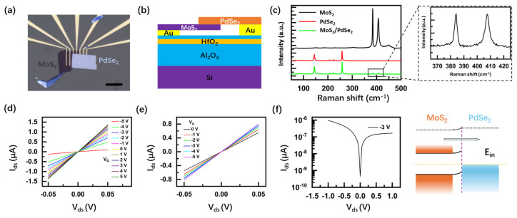
MoS2 is one of the most studied 2D materials, and it demonstrates the ability to have remarkable electronic and optoelectronic properties, which makes it a great potential photodetector candidate. Considering the large carrier density and high work function of PdSe2, a depletion region of the junction can be formed by stacking the MoS2/PdSe2 heterostructure. Multilayers of MoS2 and PdSe2 were subsequently exfoliated and stacked together (Figure 1a). The details of device fabrication are provided in Section S1 of Supplementary Materials. The schematic of the MoS2/PdSe2 photodetector is shown in Figure 1b. Figure 1c shows the distinct Raman peaks of the MoS2/PdSe2 heterostructure, which correspond to 382 cm−1 () and 407 cm−1 () for MoS2 and 144 cm−1 (), 203 cm−1 (), 222 cm−1 (), and 258 cm−1 () for PdSe2. Figure 1d and e show the Ids–Vds curves under different gate voltages VG for MoS2 and PdSe2 field-effect transistor (FET), respectively. Notably, both Ids–Vds curves demonstrate obvious linearity, and it can be proved to be Ohmic source-drain contact for both FETs, which is necessary for optoelectronic characteristics of the MoS2/PdSe2 photodetector. Furthermore, the output curves of Ids–Vds for MoS2 FET exhibit a n-type ambipolar conducting behavior at VG from −5 to 5 V. By contrast, the current slightly increases with decreasing negative VG for PdSe2 FET, which indicates the semi-metallic behavior. Given the bandgaps of multilayer MoS2 and PdSe2 are previously reported to be 1.2 and 0.03 eV [21,22], the band alignment of the MoS2/PdSe2 heterojunction is illustrated in Figure 1f. The Schottky barrier can be formed at the interface of the MoS2/PdSe2 heterojunction, and the Ids–Vds curve exhibits a rectification behavior, demonstrating a rectification ratio of Ion/Ioff up to 10.
Figure 1.
Schematics and characterization of the MoS2/PdSe2 heterostructure device: (a,b) Schematic and picture of MoS2/PdSe2 heterostructure photodetector. The scale bar is 20 μm; (c) Raman spectra of the multilayer MoS2 flakes, PdSe2 flakes, and heterostructure, respectively; (d,e) Ids–Vds relationship of MoS2 and PdSe2, respectively; (f) the transfer characteristics of the MoS2/PdSe2 heterostructure under the bias of −3 V and schematic of the MoS2/PdSe2 heterostructure-based Schottky barrier.
3. Results
3.1. Transfer Characteristics and Static Memory Behavior
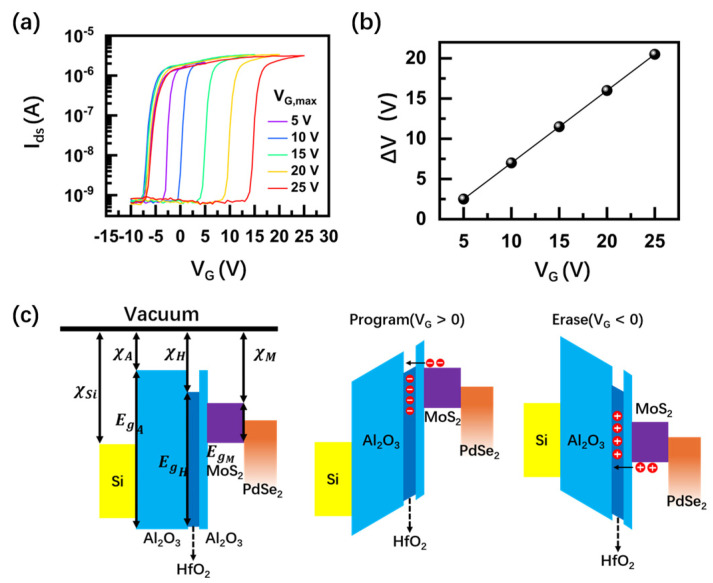
A charge-trap stack of Al2O3/HfO2/Al2O3 (6 nm/8 nm/32 nm) was deposited via atomic layer deposition (ALD). Figure 2a shows the transfer curves of the MoS2/PdSe2 Schottky diode. The transfer curves were acquired by sweeping the gate voltage VG in a closed loop (from negative to positive values) under a fixed Vds of −1 V, exhibiting a clear hysteresis window, and the hysteresis enables widening as the VG sweep range increases from 5 to 25 V. The Ids–VG curves exhibit a clockwise memory window. The extraction of memory window ∆V increases almost linearly with the maximum VG and reaches a maximum of 20 V when the VG sweeps to 25 V (Figure 2b). The transfer curve of Ids–VG decreases with increasing negative VG, suggesting that n-type MoS2 dominates the transfer characteristics of the device. Figure 2c illuminates the device operation process. When a high positive/negative VG was applied to the gate, the band alignment started favoring the tunneling in/out of electrons from the MoS2/PdSe2 channel to the HfO2 charge-trap layer, which resulted in the change of carrier concentration in MoS2 and a switch between program and erase state, respectively.
Figure 2.
The statical behavior of the nonvolatile gate charge-trap memory based on MoS2/PdSe2 heterostructure: (a) Ids–VG characteristics of the device under different VG at Vds = −1 V; (b) extraction of memory window ∆V vs. VG. The memory window increases from 1 to ∼20 V in our experimental settings; (c) band diagram of the program/erase state of the device under positive and negative VG. Positive VG programs the device. Electrons tunneling from the few-layer MoS2 channel are accumulated in the HfO2 charge-trap layer. Negative VG erases the device. Holes tunnel from the few-layer MoS2 channel to the HfO2 charge-trap layer.
3.2. Dynamic Memory Behavior of the Device
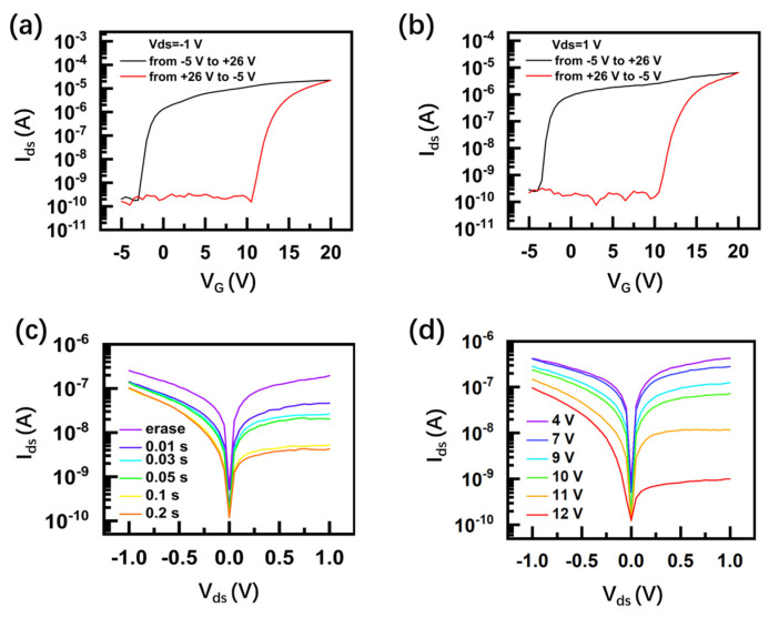
The transfer characteristics of the device are further studied under different biases. As shown in Figure 3a,b, they show that an obvious memory window occurs under both a forward bias of −1 V and a reverse bias of +1 V. A maximum program/erase current ratio of 105 can be achieved under a forward bias of −1 V. Endurance and retention time of the MoS2/PdSe2 memory are provided in Section S4 of Supplementary Materials. To explore the dynamic transition of the device, the device was initially set into an erase state by applying a negative gate pulse (−10 V, duration of 2 s). The output curves Ids–Vds were read by sweeping Vds from −1 V to +1 V after applying a series of +25 V gate pulses with different duration times. The output curve Ids–Vds shows a clear decrease and is nearly saturated when the width of the pulse increases to 0.2 s (Figure 3c). According to the expression of the charge-trapping rate [23], the calculated charge-trapping rate varies from 1015 cm−2s−1 to 1014 cm−2s−1 when the pulse width changes from 0.01 s to 0.2 s. Figure 3d shows the dependency of output curves Ids–Vds with the amplitude of the gate pulse. It demonstrates that output current decreases with the increase of pulse amplitude. This can be explained by the modulation of the Schottky barrier through the gate pulse, which also suggests that the charge-trapping mechanism of the AHA gate stack dominates the memory behavior of the device.
Figure 3.
The dynamic behavior of the nonvolatile gate charge-trap memory based on MoS2/PdSe2 heterostructure: (a,b) Ids–VG characteristics of the device under different VG under the forward bias of −1 V and reverse bias of +1 V, respectively; (c,d) Ids–Vds characteristics of the device under different pulse durations and amplitudes.
3.3. Photovoltaic Behavior and Reconfigurable Linear Polarization
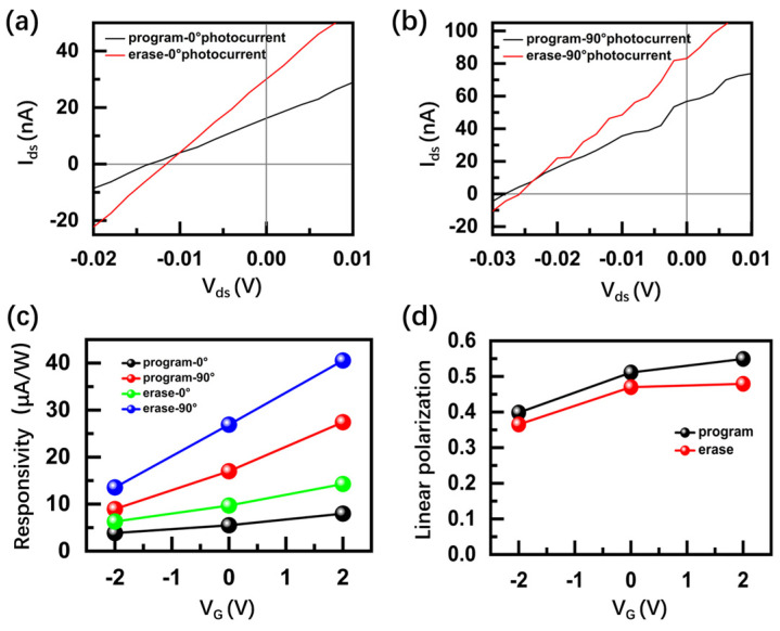
Given the excellent memory switching properties of the device (including unprecedented memory window, large program/erase current ratio, and nonvolatile switchable Schottky barriers) and strong optical anisotropy of PdSe2, the polarization-modulated photovoltaic behavior in the MoS2/PdSe2-based photodetector was worthy of investigation. To characterize it, a positive (+25 V) and negative (−10 V) gate pulse with a width of 0.2 s were applied to switch the device into the program and erase state, respectively. In the program/erase state, Ids–Vds characteristics under illumination were recorded by using the polarized 520 nm light with an intensity of 120 mW/cm2. Figure 4a,b show the Ids–Vds characteristics of the device under parallel () and vertical () polarized light in the program and erase state, respectively ( and directions correspond to the b-axis and a-axis crystalline direction of PdSe2). The crystalline orientation of PdSe2 was determined by angle-resolved polarized Raman spectroscopy (ARPRS), and details of the measurement are provided in Section S3 of Supplementary Materials. It can be noticed that the device exhibits noticeable photovoltaic responses, including a short-circuit current (Isc) of ~15 nA/30 nA and an open-circuit voltage (Voc) of ~−0.014 V/−0.012 V in the program/erase state under parallel light excitation. After switching the polarization of light to the vertical direction, the illuminated Ids–Vds curves shift toward the higher value, showing that Isc and Voc increase to ~54 nA/82 nA and ~−0.027/−0.025 V in the program/erase state. It is noted that significant photocurrent noise occurs during photocurrent measurement, which can be attributed to the degeneration of 2D flakes and environmental noise. The protection layer of Al2O3 on top of the MoS2/PdSe2 heterostructure and the optimized measurement method can significantly reduce the noise, which is summarized in Section S5 of Supplementary Materials. In addition, gate voltage was applied to modulate the performance of the device. The responsivity was extracted and plotted in Figure 4c at different memory states and polarization of light. The noise equivalent power (NEP) and detectivity of this photodetector were measured and are provided in Section S6 of Supplementary Materials. The device shows typical transfer characteristics of an n-type MoS2 semiconductor. As the gate voltage increases from −2 V to 2 V, all of the responsivities increase at Vds = −1 V. A figure of merit of the linear polarized photodetection is the degree of linear polarization (LP), where LP = (Imax − Imin)/(Imax + Imin), where Imax and Imin are the photocurrents of the detected light parallel and perpendicular to the primary polarization direction, respectively. Figure 4d shows the LP results as a function of VG. Under 120 mW/cm2 light illumination, both LP values of the device gradually increase from 0.4/0.36 to 0.55/0.49 in the program/erase state. This indicates that the LP of the device can be effectively modulated by the memory state, and its gap between the program and erase state becomes more obvious under the positive gate voltage.
Figure 4.
The polarization-modulated photovoltaic behavior of MoS2/PdSe2 photodetector: (a,b) Short-circuit current Isc and open-circuit voltage Voc of MoS2/PdSe2 photodetector under the program and erase state, respectively. (c,d) Dependency of responsibility and linear polarization with gate voltage VG under different program/erase states and polarization directions of light.
4. Discussion
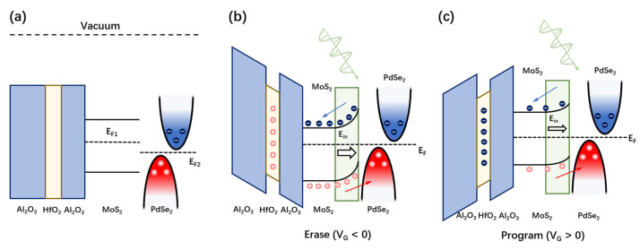
To understand the photoresponse mechanism of the MoS2/PdSe2 device, the energy band structure diagram is illustrated in Figure 5. Since the fermi level of PdSe2 is lower than MoS2, the electrons will flow from MoS2 to PdSe2, and the holes diffuse in opposite directions to MoS2. The opposite diffusion of electrons and holes introduces a Schottky barrier with the build-in field Ein pointing from MoS2 to PdSe2, which is described in Figure 1f. When the laser shines on the surface of the device, the electrons confined in the valence band will be excited by the conduction bands in both materials. Then, with the help of build-in field Ein, the electrons occupied in PdSe2 can be driven to the conduction band of MoS2, while Ein will force the holes within the MoS2 valence band to flow into the valence band of PdSe2, resulting in the photovoltaic behavior. When the negative gate voltage pulse is applied to switch the device into an erase state (Figure 5b), the energy band of MoS2 is lowered, and Ein will increase, which results in the enhancement of separation of photo-generated electron-hole pairs as well as short-circuit current. Meanwhile, the photocurrent generated from MoS2 increases in the erase state, which results in the decrease of LP because of the intrinsic polarization-insensitivity of MoS2. On the other hand, the Ein will be reduced in the program state (Figure 5c), which induces the decrease of short-circuit current and increase of LP. In this way, we can adjust the energy band structure of MoS2/PdSe2 by switching the program/erase state, thereby adjusting the photodetection performance of the device.
Figure 5.
Photoresponse mechanism of reconfigurable MoS2/PdSe2 photodetector: (a) The energy band structure of AHA charge-trap stack and MoS2/PdSe2 heterostructure before contact; (b,c) the energy band structure of the device and the flow of photo-generated electron-holes under illumination when the device is set to erase (VG < 0) and program states (VG > 0), respectively.
5. Conclusions
In summary, a multifunctional photovoltaic photodetector was demonstrated, which was composed of in-plane anisotropic PdSe2 and MoS2 with an AHA charge-trap gate stack. The device exhibits a nonvolatile phenomenon in both electrical and photovoltaic characteristics, resulting from the modulation of band alignment by the gate voltage pulse. Utilizing the AHA charge-trap gate stack, the memory window and program/erase current ratio of MoS2/PdSe2 can be effectively modulated. Acting as a reconfigurable polarimetric photodetector, the device exhibits a reversible performance of both responsivity and polarization-sensitive photocurrent by switching the program and erase state, rendering it a promising candidate for polarization signal recognition and imaging.
Supplementary Materials
The following supporting information can be downloaded at https://www.mdpi.com/article/10.3390/nano14231936/s1: Figure S1. Thickness of (a) MoS2 and (b) PdSe2 measured by atomic force microscopy. Figure S2. Angle-resolved polarized Raman spectroscopy of a PdSe2 flake. Figure S3. Endurance of the MoS2/PdSe2 memory. (a) Endurance of the memory device for 100 cycles with the program/erase voltage being +20 V, 1 s and −10 V, 1 s. (b) The stability of the program/erase state of the device after programming at +20 V, 1 s duration, and erasing at −10 V, 1 s duration (Vds = -1 V). Figure S4. The polarization-modulated photovoltaic behavior of the MoS2/PdSe2 photodetector.: (a) and (b) Short-circuit current Isc and open-circuit voltage Voc of the MoS2/PdSe2 photodetector under the program and erase state, respectively. Figure S5. The NEP and detection limit of the MoS2/PdSe2 photodetector. (a) NEP and (b) detectivity tuned by the gate voltage, indicating the detection limit of our photodetector.
Author Contributions
C.G. and X.H. conceived the research, and Q.B. and T.L. fabricated the samples. Q.B. conducted the measurements. X.H., Q.B., Y.G., Q.L., T.L., W.L., A.J., B.Q., H.Y., B.L. and C.G. discussed the data and contributed to the manuscript. All authors have read and agreed to the published version of the manuscript.
Data Availability Statement
The data presented in this study are available on request from the corresponding author.
Conflicts of Interest
The authors declare no conflicts of interest.
Funding Statement
This work was supported by the National Natural Science Foundation of China under Grant Nos. 62204259, 92265110, 62174179, 11974386, and 61905274, the National Key Research and Development Program of China under Grant Nos. 2024YFA1207700, 2022YFA1204100, and 2021YFA1400700, Strategic Priority Research Program of the Chinese Academy of Sciences under Grant No. XDB33020200, and the Guangdong Basic and Applied Basic Research Foundation under Grant No. 2023A1515010693. This work was also supported by the Micro/nano Fabrication Laboratory of Synergetic Extreme Condition User Facility (SECUF).
Footnotes
Disclaimer/Publisher’s Note: The statements, opinions and data contained in all publications are solely those of the individual author(s) and contributor(s) and not of MDPI and/or the editor(s). MDPI and/or the editor(s) disclaim responsibility for any injury to people or property resulting from any ideas, methods, instructions or products referred to in the content.
References
- 1.Hou H.Y., Tian S., Ge H.R., Chen J.D., Li Y.Q., Tang J.X. Recent progress of polarization-sensitive perovskite photodetectors. Adv. Funct. Mater. 2022;32:2209324. doi: 10.1002/adfm.202209324. [DOI] [Google Scholar]
- 2.Wu D., Guo J., Du J., Xia C., Zeng L., Tian Y., Shi Z., Tian Y., Li X.J., Tsang Y.H. Highly polarization-sensitive, broadband, self-powered photodetector based on graphene/PdSe2/germanium heterojunction. ACS Nano. 2019;13:9907–9917. doi: 10.1021/acsnano.9b03994. [DOI] [PubMed] [Google Scholar]
- 3.Wang J., Jiang C., Li W., Xiao X. Anisotropic low-dimensional materials for polarization-sensitive photodetectors: From materials to devices. Adv. Opt. Mater. 2022;10:2102436. doi: 10.1002/adom.202102436. [DOI] [Google Scholar]
- 4.Guo Z., Cao R., Wang H., Zhang X., Meng F., Chen X., Gao S., Sang D.K., Nguyen T.H., Duong A.T. High-performance polarization-sensitive photodetectors on two-dimensional β-InSe. Natl. Sci. Rev. 2022;9:nwab098. doi: 10.1093/nsr/nwab098. [DOI] [PMC free article] [PubMed] [Google Scholar]
- 5.Huo N., Konstantatos G. Recent progress and future prospects of 2D-based photodetectors. Adv. Mater. 2018;30:1801164. doi: 10.1002/adma.201801164. [DOI] [PubMed] [Google Scholar]
- 6.Zhou C., Zhang S., Lv Z., Ma Z., Yu C., Feng Z., Chan M. Self-driven WSe2 photodetectors enabled with asymmetrical van der Waals contact interfaces. npj 2D Mater. Appl. 2020;4:46. doi: 10.1038/s41699-020-00179-9. [DOI] [Google Scholar]
- 7.Qiu Q., Huang Z. Photodetectors of 2D materials from ultraviolet to terahertz waves. Adv. Mater. 2021;33:2008126. doi: 10.1002/adma.202008126. [DOI] [PubMed] [Google Scholar]
- 8.Zhou Z., Long M., Pan L., Wang X., Zhong M., Blei M., Wang J., Fang J., Tongay S., Hu W. Perpendicular optical reversal of the linear dichroism and polarized photodetection in 2D GeAs. ACS Nano. 2018;12:12416–12423. doi: 10.1021/acsnano.8b06629. [DOI] [PubMed] [Google Scholar]
- 9.Yuan H., Liu X., Afshinmanesh F., Li W., Xu G., Sun J., Lian B., Curto A.G., Ye G., Hikita Y. Polarization-sensitive broadband photodetector using a black phosphorus vertical p–n junction. Nat. Nanotechnol. 2015;10:707–713. doi: 10.1038/nnano.2015.112. [DOI] [PubMed] [Google Scholar]
- 10.Liu F., Zheng S., He X., Chaturvedi A., He J., Chow W.L., Mion T.R., Wang X., Zhou J., Fu Q. Highly sensitive detection of polarized light using anisotropic 2D ReS2. Adv. Funct. Mater. 2016;26:1169–1177. doi: 10.1002/adfm.201504546. [DOI] [Google Scholar]
- 11.Li L., Gong P., Sheng D., Wang S., Wang W., Zhu X., Shi X., Wang F., Han W., Yang S. Highly in-plane anisotropic 2D GeAs2 for polarization-sensitive photodetection. Adv. Mater. 2018;30:1804541. doi: 10.1002/adma.201804541. [DOI] [PubMed] [Google Scholar]
- 12.Wang X., Shang J., Zhu M., Zhou X., Hao R., Sun L., Xu H., Zheng J., Lei X., Li C. Controlled growth of large-scale uniform 1T′-MoTe2 crystals with tunable thickness and their photodetector applications. Nanoscale Horiz. 2020;5:954–959. doi: 10.1039/D0NH00075B. [DOI] [PubMed] [Google Scholar]
- 13.Xu Z., Luo B., Chen Y., Li X., Chen Z., Yuan Q., Xiao X. High sensitivity and anisotropic broadband photoresponse of Td-WTe2. Phys. Lett. A. 2021;389:127093. doi: 10.1016/j.physleta.2020.127093. [DOI] [Google Scholar]
- 14.Ahn J., Ko K., Kyhm J.-h., Ra H.-S., Bae H., Hong S., Kim D.-Y., Jang J., Kim T.W., Choi S. Near-infrared self-powered linearly polarized photodetection and digital incoherent holography using WSe2/ReSe2 van der Waals heterostructure. ACS Nano. 2021;15:17917–17925. doi: 10.1021/acsnano.1c06234. [DOI] [PubMed] [Google Scholar]
- 15.Xiong J., Dan Z., Li H., Li S., Sun Y., Gao W., Huo N., Li J. Multifunctional GeAs/WS2 heterojunctions for highly polarization-sensitive photodetectors in the short-wave infrared range. ACS Appl. Mater. Inter. 2022;14:22607–22614. doi: 10.1021/acsami.2c03246. [DOI] [PubMed] [Google Scholar]
- 16.Jiang J., Xu W., Guo F., Yang S., Ge W., Shen B., Tang N. Polarization-resolved near-infrared PdSe2 pin homojunction photodetector. Nano Lett. 2023;23:9522–9528. doi: 10.1021/acs.nanolett.3c03086. [DOI] [PubMed] [Google Scholar]
- 17.Huang M., Luo S., Qiao H., Yao B., Huang Z., Wang Z., Bao Q., Qi X. Ferroelectric polarization enhanced photodetector based on layered NbOCl2. Small Sci. 2024;4:2300246. doi: 10.1002/smsc.202300246. [DOI] [Google Scholar]
- 18.Wu G., Zhang X., Feng G., Wang J., Zhou K., Zeng J., Dong D., Zhu F., Yang C., Zhao X. Ferroelectric-defined reconfigurable homojunctions for in-memory sensing and computing. Nat. Mater. 2023;22:1499–1506. doi: 10.1038/s41563-023-01676-0. [DOI] [PubMed] [Google Scholar]
- 19.Zhou G., Li J., Song Q., Wang L., Ren Z., Sun B., Hu X., Wang W., Xu G., Chen X. Full hardware implementation of neuromorphic visual system based on multimodal optoelectronic resistive memory arrays for versatile image processing. Nat. Commun. 2023;14:8489. doi: 10.1038/s41467-023-43944-2. [DOI] [PMC free article] [PubMed] [Google Scholar]
- 20.Zhang G.-X., Zhang Z.-C., Chen X.-D., Kang L., Li Y., Wang F.-D., Shi L., Shi K., Liu Z.-B., Tian J.-G. Broadband sensory networks with locally stored responsivities for neuromorphic machine vision. Sci. Adv. 2023;9:eadi5104. doi: 10.1126/sciadv.adi5104. [DOI] [PMC free article] [PubMed] [Google Scholar]
- 21.Long M., Wang Y., Wang P., Zhou X., Xia H., Luo C., Huang S., Zhang G., Yan H., Fan Z. Palladium diselenide long-wavelength infrared photodetector with high sensitivity and stability. ACS Nano. 2019;13:2511–2519. doi: 10.1021/acsnano.8b09476. [DOI] [PubMed] [Google Scholar]
- 22.Kang J., Tongay S., Zhou J., Li J., Wu J. Band offsets and heterostructures of two-dimensional semiconductors. Appl. Phys. Lett. 2013;102:012111. doi: 10.1063/1.4774090. [DOI] [Google Scholar]
- 23.Sup Choi M., Lee G.-H., Yu Y.-J., Lee D.-Y., Hwan Lee S., Kim P., Hone J., Jong Yoo W. Controlled charge trapping by molybdenum disulphide and graphene in ultrathin heterostructured memory devices. Nat. Commun. 2013;4:1624. doi: 10.1038/ncomms2652. [DOI] [PubMed] [Google Scholar]
Associated Data
This section collects any data citations, data availability statements, or supplementary materials included in this article.
Supplementary Materials
Data Availability Statement
The data presented in this study are available on request from the corresponding author.


