ABSTRACT
Computational approaches using theoretical calculations and data scientific methods have become increasingly important in materials science and technology, with the development of relevant methodologies and algorithms, the availability of large materials data, and the enhancement of computer performance. As reviewed herein, we have developed computational methods for the design and prediction of inorganic materials with a particular focus on the exploration of semiconductors and dielectrics. High-throughput first-principles calculations are used to systematically and accurately predict the local atomic and electronic structures of polarons, point defects, surfaces, and interfaces, as well as bulk fundamental properties. Machine learning techniques are utilized to efficiently predict various material properties, construct phase diagrams, and search for materials satisfying target properties. These computational approaches have elucidated the mechanisms behind material functionalities and explored promising materials in combination with synthesis, characterization, and device fabrication. Examples include the development of ternary nitride semiconductors for potential optoelectronic and photovoltaic applications, the exploration of phosphide semiconductors and the optimization of heterointerfaces toward the improvement of phosphide-based photovoltaic cells, and the discovery of ferroelectricity in layered perovskite oxides and the theoretical understanding of its origin, all of which demonstrate the effectiveness of our computer-aided materials research.
KEYWORDS: Semiconductors, dielectrics, photovoltaics, phase diagrams, first-principles calculations, machine learning
GRAPHICAL ABSTRACT
IMPACT STATEMENT
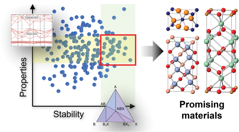
The developed first-principles and machine-learning approaches in conjunction with experiments accelerate the design and exploration of new semiconductors and dielectrics.
1. Introduction
Inorganic semiconductors and dielectrics are essential components of electronic and optoelectronic devices in modern society. To meet the demands for further improvement of the material and device performance, not only the optimization of device structures but also the exploration of novel materials with superb properties is needed, particularly for innovating new applications [1–8]. However, the search for as-yet-unknown or as-yet-unused materials with desired properties and sufficient stability is generally challenging. It typically requires huge efforts and costs for a series of experiments from synthesis, crystal- and micro-structure characterization, and property measurements to device fabrication and optimization.
Computational approaches using theoretical calculations and data scientific methods can be helpful to accelerate such materials research if they allow us to make reliable predictions. With the development of methodologies and algorithms and the enhancement of computer performance, theoretical calculations such as first-principles calculations are applicable to a wider variety of material issues and, therefore, play increasingly important roles nowadays [9–13]. Data scientific methods such as machine learning are being spread in the field of materials science and technology, as larger data becomes available [14–16]. Several computational databases are already open to the public and widely used in materials research. Examples include the Material Project [17], AFLOW Distributed Materials Property Repository [18], Open Quantum Materials Database (OQMD) [19], Electronic Structure Project (ESP) [20], Open Materials Database [21], Materials Cloud [22], and Novel Materials Discovery (NOMAD) Repository [23]. Efforts to construct open experimental databases for inorganic materials have also been made [24,25].
To deploy such theoretical calculations, machine learning, and their combinations in a broader variety of materials studies, further development of methodologies and algorithms is desired. In particular, high-quality and large datasets are key to the effective use of machine learning. First-principles calculations are able to generate data on diverse material properties, including the atomic and electronic structures and related properties of perfect crystals, amorphous phases, point defects, dislocations, surfaces, grain boundaries, and heterointerfaces. However, the prediction accuracy and the computational efficiency of first-principles calculations are usually in a trade-off relationship. This issue particularly matters when we deal with imperfect crystals that require the use of large simulation models and the consideration of various configurations. It is essential to develop accurate but efficient computational schemes to overcome this situation. Moreover, the development of new materials should be accelerated if reliable computational screening of a tremendous number of candidate materials is doable and combined with experiments appropriately.
In this article, we review our combined computational and experimental approaches to inorganic semiconductors and dielectrics. In Sec. 2, we describe the first-principles calculation methods that allow for accurate and efficient prediction of various material properties, not only bulk electronic structures and relevant fundamental properties but also the formation energies, geometries, and electronic structures of polarons, point defects including native defects and dopants, surfaces, and interfaces. As a novel machine learning approach, we emphasize an efficient construction of phase diagrams with the aid of active learning. The applications of these computational methods to various materials research issues are also shown, where first-principles calculations, machine learning techniques, and/or experiments are combined to accelerate the prediction of material properties, the exploration of materials with desired properties, and the suggestion of synthesis conditions. In Sec. 3, we discuss the design and exploration of new semiconductors and dielectrics by combining experimental and computational approaches. This includes the development of nitride and phosphide semiconductors for optoelectronic and photovoltaic applications, followed by phosphide-based photovoltaic cell fabrication, and the discovery of new layered perovskite oxide ferroelectrics. The origins of their functionalities have been elucidated with the support of electronic structure and chemical bonding analyses using the first-principles calculations. We then summarize our work and provide an outlook on computer-aided materials research in Sec. 4.
2. Development and application of computational methods for predicting the structures, properties, and phase diagrams of semiconductors and dielectrics
2.1. First-principles approaches to polarons, point defects, surfaces, and interfaces
We have developed computational methods based on first-principles calculations to predict the formation energies and the local atomic and electronic structures of polarons [26–28], point defects [28–39], dislocations [40], surfaces [41–49], and interfaces [40,41,44,46,50,51], as well as bulk fundamental properties and stability [41,44,52–58], accurately and/or efficiently. The first-principles calculations are conducted using the projector augmented-wave method [59] as implemented in the Vienna Ab initio Simulation Package [60,61]. Appropriate corrections have been applied to overcome the limitations in the description of the electronic structure [26,34,44,62] and the restriction in the simulation cell size [30,63]. The construction of simulation models and calculation processes are automated to enable high-throughput calculations [34,35,42,45,55]. Such approaches are briefly described below with an emphasis on the case of surfaces.
Inorganic semiconductors and dielectrics, which are our main targets, have finite band gaps, as well as insulators. It is well known that standard exchange-correlation functionals such as the local (spin) density approximation (L(S)DA) [64–66] and the generalized gradient approximation (GGA) [67–70] to density functional theory [71] tend to underestimate band gaps of many systems. In addition, localized states in solids are not well described by these approximations [13,52,72,73]. This drawback can be concisely remedied using Hubbard U corrections, so-called L(S)DA+U and GGA+U, when the localized states mainly originate from particular atomic orbitals [72,73]. To better describe the overall electronic structures of semiconductors, dielectrics, and insulators, hybrid functionals that partially incorporate the non-local Fock exchange are often used nowadays [74–77]. However, the results depend on the form and parameters in hybrid functionals such as the mixing amount of the Fock exchange, the optimal value of which by nature depends on the electronic structures of the systems of interest because of the system-dependent screening behavior [74,78,79]. Dielectric-dependent hybrid functionals are often effective in overcoming this issue, a concise form of which uses the Fock exchange mixing value determined from the electronic contributions to the dielectric constants calculated for materials of interest [78,80,81]. This approach has been reported to well reproduce the band gaps of prototypical semiconductors and insulators [78,80,81].
Hybrid functional calculations are computationally demanding, particularly when dealing with polarons, dislocations, point defects, surfaces, and interfaces using supercells. If reasonably applicable, we conduct dielectric-dependent hybrid functional calculations non-self-consistently on top of the GGA or GGA+U. For prototypical materials, we have shown that this approach dramatically accelerates electronic structure calculations with sufficient accuracy preserved [34,44,45,49,82]. Examples of band gap predictions for prototypical semiconductors and insulators are shown in Figure 1 [44].
Figure 1.
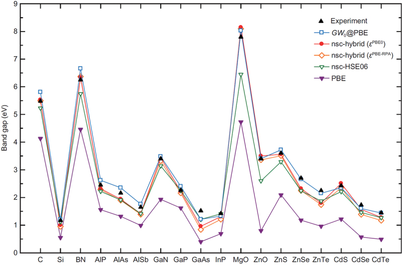
Band gaps of prototypical semiconductors and insulators from first-principles calculations using various approximations, including non-self-consistent (nsc) dielectric-dependent hybrid functional approaches, compared with reported experimental values. Adapted with permission from ref. [44]. Copyright 2017 American physical society.
The GW [83] and related approximations based on many-body perturbation theory enable us to obtain quasi-particle band structures. For prototypical systems with relatively simple band structures, the band gaps are well reproduced using standard GW calculations on top of the GGA, as shown in Figure 1. However, the accuracy depends significantly on the level of the approximations for other properties such as localized semi-core states, ionization potentials (IPs), and electronic affinities (EAs) [41,52], as well as the case of materials with more complicated band structures [84]. Calculations using a high level of the GW approximation and beyond are rather computationally demanding and, therefore, not suited to high-throughput data generation. In our study that aims at data-driven approaches, we have occasionally used GW calculations to check the results of GGA(+U) and hybrid functional calculations.
The non-self-consistent hybrid functional approach allows us to make band-edge corrections to the GGA(+U) results by utilizing the fact that electrostatic potentials do not change from the input GGA(+U) values. This feature is advantageous in the accelerated evaluation of the formation energies and electronic levels of polarons and point defects if the polaron and defect states are reasonably described using the GGA(+U) [34,85–88]; otherwise, we use self-consistent hybrid functional calculations even though they are computationally rather demanding.
Surface band-edge positions with respect to the vacuum level, namely IPs and EAs, and interfacial band offsets are also efficiently evaluated using the non-self-consistent hybrid functional approach. In typical evaluation procedures for the surface and interface band positions, the results for surface or interface and bulk models are combined through the electrostatic alignment [13]. This is schematically shown in Figure 2 [49]. Here, standard self-consistent hybrid functional calculations of surfaces and interfaces are computationally expensive in many cases. Overall computational costs are dramatically reduced if the bulk electronic structures are obtained using non-self-consistent hybrid functional calculations on top of the GGA(+U) and electrostatically aligned with the surface or interface results treated using the GGA(+U) [44].
Figure 2.
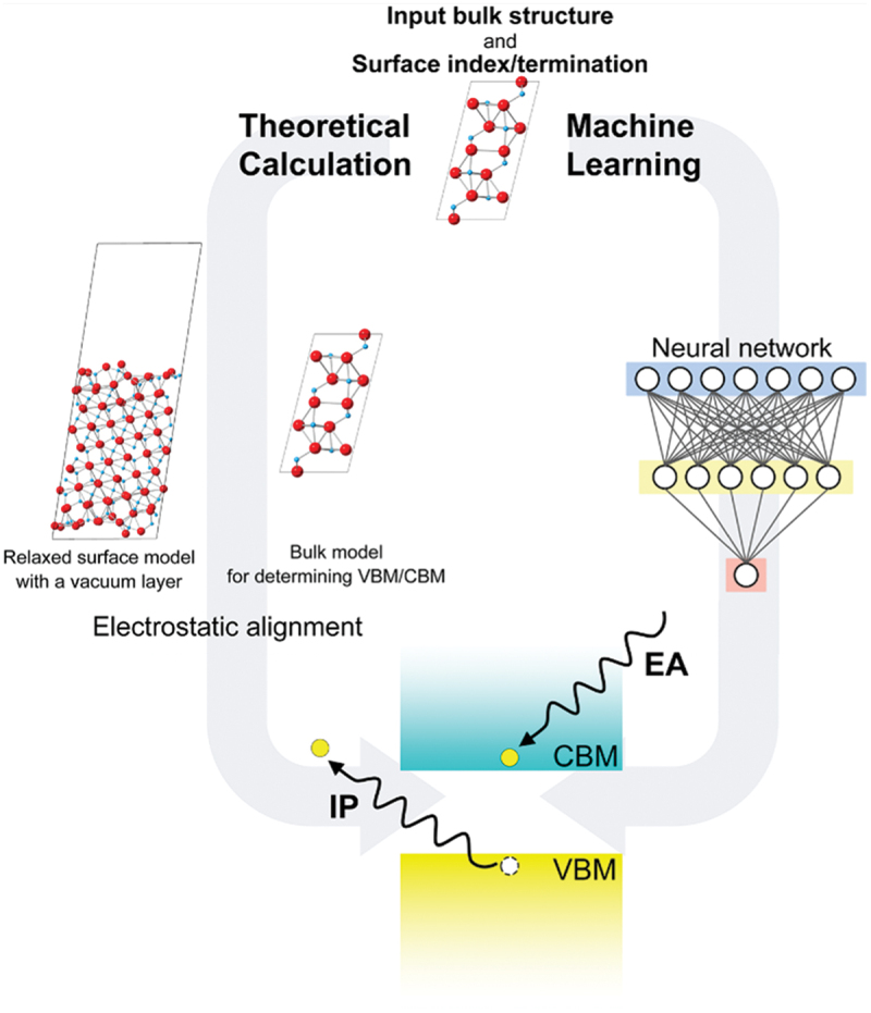
Schematic showing the computational procedures for the evaluation of IPs and EAs of non-metallic solids. Two approaches using theoretical (first principles) calculations and machine learning (neural network) are illustrated. Reprinted from ref. [49] under a creative commons attribution 4.0 international license.
In combination with an algorithm for automatic non-polar surface model generation [42], we have conducted first-principles calculations of in total about 3000 surface models for non-metallic binary and ternary oxides using the aforementioned non-self-consistent dielectric-dependent hybrid functional approach [49]. The resultant IPs and EAs for 2195 binary oxide surfaces are shown in Figure 3 [49]. The upper panel includes the results for various polymorphs and surface orientations, and the IPs and EAs are widely spread even within the common cation species. Still, we can see some chemical trends related to the group and period of the constituent element (cation) in the periodic table. The lower panel shows a comparison with reported experimental values. The IPs and EAs of solids, by nature, depend on the surface atomic structures and, therefore, the surface orientation, termination plane, reconstruction, adsorption, and contamination, all of which affect the surface dipole contributions [89–93]. Ideally speaking, identical surfaces should be considered for the experiments and theoretical calculations. However, available experimental values are limited for oxides, especially for well-characterized surfaces at the atomistic level. Nevertheless, reasonable agreement is found between theory and experiment overall. Our previous study has found that the non-self-consistent dielectric-dependent hybrid functional calculations can reproduce experimental values better in the case of prototypical semiconductors with surface atomic structures reported [44], for which a direct comparison between theory and experiment is more straightforward and meaningful. In addition, highly accurate prediction of the IPs and EAs requires a rather sophisticated approximation, for instance, the GWΓ1 approach based on many-body perturbation theory [41,52]. Given that such calculations are computationally demanding even for systems with small unit cells, we believe that the non-self-consistent dielectric-dependent hybrid functional approach is a well-balanced scheme suited for high-throughput studies.
Figure 3.
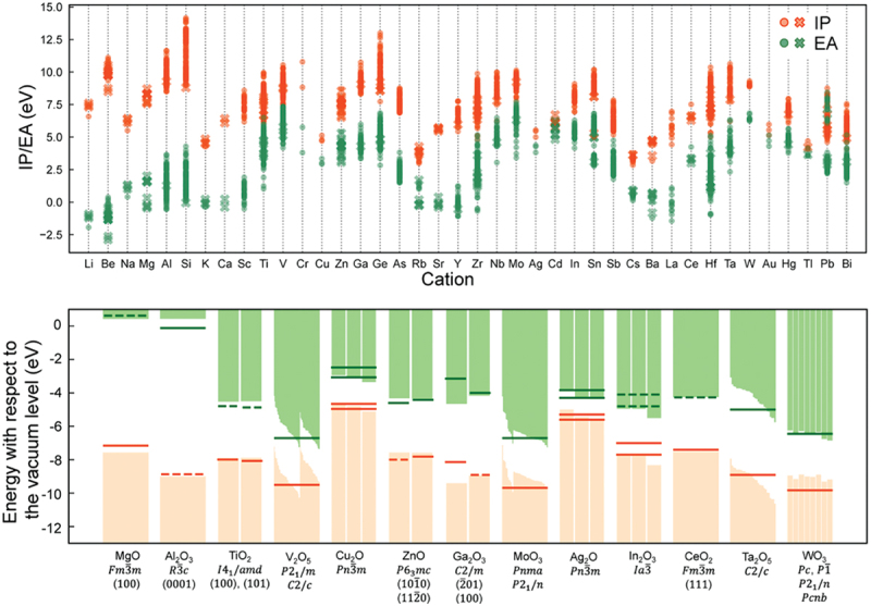
Theoretical IPs and EAs for 2195 nonpolar surfaces of binary oxides obtained using non-self-consistent dielectric-dependent hybrid functional calculations. A comparison with reported experimental values is given in the lower panel, where the negatives of the IPs and EAs corresponding to the valence band maxima and conduction band minima against the vacuum level, respectively, are plotted. The experimental values are indicated by horizontal solid and broken bars. The theoretical values for various polymorphs and surface orientations are included when the experimentally investigated crystal structures and/or surface orientations have not been specified. Reprinted from ref. [49] under a creative commons attribution 4.0 international license.
In the above, we consider the cases where atomic relaxation is not significant at the surfaces. In reality, however, surfaces often show complicated and dramatic structural reconstructions [94–98]. As a case study, we have modeled macroscopically stoichiometric and nonpolar reconstructed (001) surfaces of A(I)B(V)O3 (NaTaO3, KNbO3, and KTaO3), A(II)B(IV)O3 (CaTiO3, SrTiO3, BaTiO3, and BaZrO3), and A(III)B(III)O3 (YAlO3, LaAlO3, and LaGaO3) perovskites using a combination of first-principles calculations and an evolutionary algorithm [43,47]. Four types of representative reconstructed patterns were obtained with diverse atomic arrangements, as illustrated in Figure 4(a) [47]; here, the cation exchange structure has reproduced the previously predicted one for KTaO3 [99]. Significant dependency of the valence band maximum (VBM) and the conduction band minimum (CBM) relative to the vacuum level (the negatives of IPs and EAs, respectively) on both composition and reconstructed structure is recognized in Figure 4(b), which is explainable in terms of the atomic configurations near the surfaces [47]: the decrease of the coordination number of cation A (B) at the surfaces leads to shallow (deep) VBMs and CBMs relative to the vacuum level. This chemical trend is clarified using relative coordination number ratio , where and are the coordination numbers of cation A (B) at the surface and the bulk, respectively.
Figure 4.
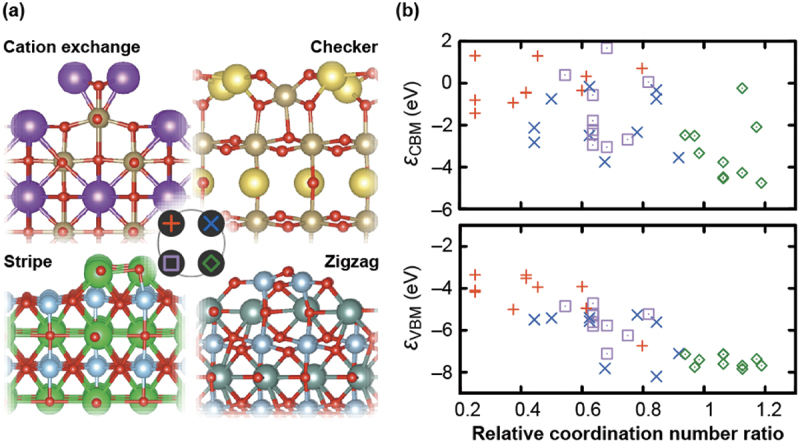
(a) Reconstructed structures of macroscopically stoichiometric and nonpolar (001) surfaces of A(I)B(V)O3 (NaTaO3, KNbO3, and KTaO3), A(II)B(IV)O3 (CaTiO3, SrTiO3, BaTiO3, and BaZrO3), and A(III)B(III)O3 (YAlO3, LaAlO3, and LaGaO3) perovskites predicted using a combination of first-principles calculations and an evolutionary algorithm. Four types of representative reconstructed structures are shown: cation-exchange, checker, stripe, and zigzag models, which are labeled with red plus, blue cross, purple square, and green diamond marks, respectively. (b) CBM and VBM relative to the vacuum level (εCBM and εVBM, respectively) as a function of relative coordination number (see texts for details). Reprinted from ref. [47] under a creative commons attribution 4.0 international license.
Other computational methodologies developed include those for predicting the band positions at polar surfaces and interfaces using slab models with appropriate pseudo-hydrogen passivation [46].
2.2. Combination of first-principles calculations and machine learning to accelerate material-property prediction and materials exploration
Needless to say, machine-learning models can be effective in accelerating the prediction of various material properties, the exploration of target materials for diverse purposes, and so forth. Since the assessment of the accuracy and efficiency of the surrogate models particularly matters here, we mainly discuss the accuracy of our property prediction models in this section, as well as the efficiency of our models for exploring materials with desired properties and assisting the construction of phase diagrams.
Once a reasonably accurate and large dataset is obtained from first-principles calculations, machine learning can be powerful if appropriate descriptors are available. We have constructed accurate and efficient prediction models using machine learning techniques for bulk fundamental properties such as band gaps and dielectric constants [55]. Moreover, point defect and surface properties can also be predicted with sufficient accuracy using high-throughput first-principles calculation datasets [34,49]. Examples include the prediction models of the IPs and EAs of binary oxide surfaces shown in Figure 5 [49]. An artificial neural network with an attention layer is constructed for each of the IP and EA cases using the smooth overlap of atom positions as structural descriptors [100]. Assuming that the atomic relaxation does not significantly alter the structures of ideally cleaved surfaces, only the information on the bulk composition and crystal structure and the surface orientation and termination plane, namely the surface structure before relaxation, is inputted, as illustrated in Figure 2. The coefficients of determination, root mean squared errors, and mean absolute errors of the test data are given in the caption of Figure 5. All the values indicate good prediction accuracy for IPs and EAs at relaxed surfaces, despite the fact that IPs and EAs are complicated surface structure-dependent electronic properties as mentioned above.
Figure 5.
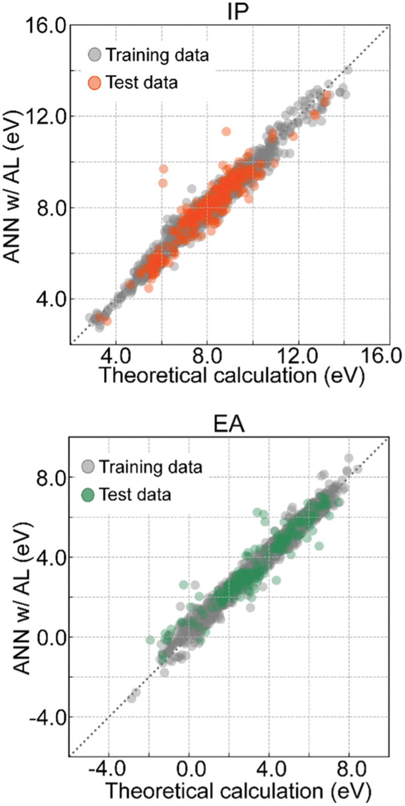
IPs and EAs of binary oxide surfaces by first-principles calculations versus those predicted by the artificial neural network with an attention layer (ANN w/AL). The coefficients of determination, root mean squared errors, and mean absolute errors of the test data are 0.90, 0.29 eV, and 0.21 eV for the IPs, and 0.93, 0.27 eV, and 0.19 eV for the EAs, respectively. Reprinted from ref. [49] under a creative commons attribution 4.0 international license.
A combination of first-principles calculations and machine learning is also a powerful scheme for materials exploration. Adaptive sampling or black-box optimization methods are widely used, including Bayesian optimization to search for the global maxima or minima of target material properties [101]. However, maximizing or minimizing material properties is not always required; there are also demands for exploring materials whose properties fall in target ranges. For this purpose, it is useful to set the acquisition function based on the probability that a data point achieves a target property within a specific range (PTR) [102]. We have implemented PTR acquisition functions in our material exploration code, including their extension to multi-objective ones, and conducted extensive performance tests [103]. Figure 6 shows examples of materials exploration simulations for two kinds of target conditions for the band gap and formation energy [103]. In both cases of Figure 6(a,b), target materials are quickly found when both the band gap and formation energy are considered using the multi-objective PTR acquisition function.
Figure 6.
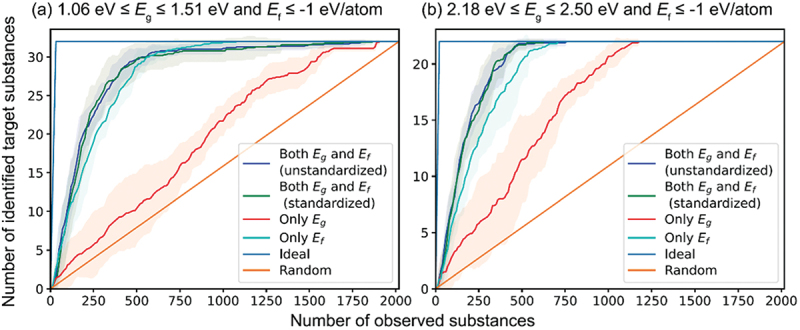
Performance of multi-objective adaptive sampling methods in the search for substances satisfying the respective conditions of the band gap (Eg) and formation energy (Ef) given in panels (a) and (b). Lines and shaded regions indicate the average and standard deviation of 10 simulations using different initial datasets, respectively. Reprinted from ref. [103] under a creative commons attribution 4.0 international license.
It is also interesting to search for exceptional materials whose chemical compositions, structures, and/or properties do not follow typical trends, given that such materials may have exceptionally good properties. The Bound Objective-free eXploration (BLOX) method has been suggested to efficiently identify exceptional materials [104]. The effectiveness of BLOX has been demonstrated through the exploration simulations of molecules [104] and solids [105] with out-of-trend properties.
Understanding the tendency of a large number of materials would be helpful in constructing new principles for materials design and exploration. Interpreting the machine learning prediction models in terms of important features is one useful approach. Clustering is also widely used to classify materials into groups according to particular features, supporting us in overviewing large material data. Typical clustering approaches consider either target material properties or fundamental features related to chemical compositions and crystal structures. The relationships between the former and the latter are unclear, preventing us from understanding the chemical and structural origins of the material properties. In this context, we have conceived a novel clustering method that simultaneously considers target material properties and fundamental chemical and structural features, enabling us to classify materials depending on the properties of our interest [106].
2.3. Prediction of phase diagrams using machine learning techniques
We have also developed methods to accelerate the investigation of phase diagrams and to predict them. Although phase diagrams are crucial in materials research, suitable machine learning techniques to assist with their determination have not been much considered.
As mentioned above, a prominent method for optimizing material properties is Bayesian optimization in the materials science community [101]. This approach effectively suggests new materials with tailored properties. However, the direct application of Bayesian optimization to phase diagram construction is impossible. Therefore, we have introduced a new machine learning strategy, uncertainty sampling [107], which is tailored to study phase diagrams in detail. Uncertainty sampling assumes that the most uncertain points contain the most valuable information. Applied to phase diagram construction, it suggests the next experimental conditions for synthesis or measurement, which are crucial for an accurate determination. The developed method is called Phase Diagram Construction (PDC) and is outlined in Figure 7 [107]. In Sec. 2.3.1, the details of the PDC algorithm are introduced. In Sec. 2.3.2, the results of applications of the PDC algorithm for known and unknown phase diagrams are shown. Improvements of the PDC algorithm are discussed in Sec. 2.3.3. Finally, in Sec. 2.3.4, a complementary method to the PDC algorithm is considered, namely a machine learning method combined with CALPHAD (CALculation of PHAse Diagrams) [108] databases to predict unknown phase diagrams.
Figure 7.
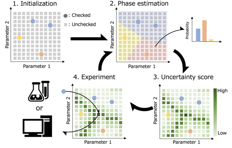
Procedure of the PDC algorithm to efficiently construct phase diagrams. Reprinted from ref. [107] under a creative commons attribution 4.0 international license.
2.3.1. PDC algorithm
The following is a detailed procedure of the PDC algorithm [107].
Step 1: initialization. We define the space where the phase diagram is to be constructed and discretize it. Each discretized point in the phase diagram serves as candidate experimental conditions. There are no restrictions on the dimensions of the phase diagram. Let denote the vector of discretized positions, and candidate points are prepared. From these, phase equilibria are identified for initial points through experiments or simulations. These initial points can be chosen randomly or according to specific rules (e.g. selecting points that are easy to conduct experiment). Existing databases can also be utilized. Discrete indices are assigned to the identified phase regions at this stage. For instance, if there are different phase regions identified initially, we prepare indices and assign these indices as labels to each data point. This process prepares the training data .
Step 2: phase diagram estimation. Using machine learning techniques such as label propagation (LP) or label spreading (LS), we estimate the probabilities of belonging to each phase region for all points in the phase diagram when is the training data. LP maintains the phase information unchanged for the points where phases are already identified, whereas LS allows phase information to vary based on the surrounding environment. Utilizing these probabilities , we can predict the phase diagram by selecting the phase region with the highest probability at each point.
Step 3: uncertainty score. We define an uncertainty score using the probabilities . We choose the next candidate where is maximum using the following equation:
| (1) |
In the PDC algorithm, three types of scores are available for the uncertainty score definition, namely the least confident (LC) method, margin sampling (MS) method, and entropy-based approach (EA):
| (2) |
| (3) |
| (4) |
where and represent the highest and second highest probabilities of phase regions at the point , respectively.
Step 4: experiment. We perform experiments or simulations at the point selected in Step 3 where the uncertainty score is maximum, and we identify the phase region at this point. If a new phase region is discovered, the phase index is increased by one as with . This process adds one more data point to the training dataset as . This dataset is utilized to return to Step 2.
This iterative process enables the construction of an accurate phase diagram with fewer iterations, leveraging uncertainty sampling to efficiently guide experimental or simulation efforts toward discovering new phases and determining phase boundaries in the phase diagram.
2.3.2. Examples of phase diagram constructions
First, to verify the efficiency of the PDC algorithm, known phase diagrams were virtually constructed. The examples include the low-pressure and high-pressure phase diagrams of water, as well as the liquidus projection of the SiO2-Al2O3-MgO pseudo-ternary system [107]. We found that using the PDC algorithm, the number of experiments required to determine a phase diagram can be reduced by a factor of five compared with random sampling. Figure 8 shows the results for each sampling method [107]. In this result, we utilized the LP method for phase diagram estimation and applied the LC approach for uncertainty score evaluation. With the PDC algorithm, the selected points were concentrated near phase boundaries, demonstrating efficient determination of phase boundaries. Moreover, the PDC algorithm found narrow phase regions quickly. We confirmed that even with a small number of initial data points (when many phases are still unidentified), the PDC algorithm efficiently produces phase diagrams. This illustrates that PDC is effective for investigating complex unknown phase diagrams from scratch.
Figure 8.
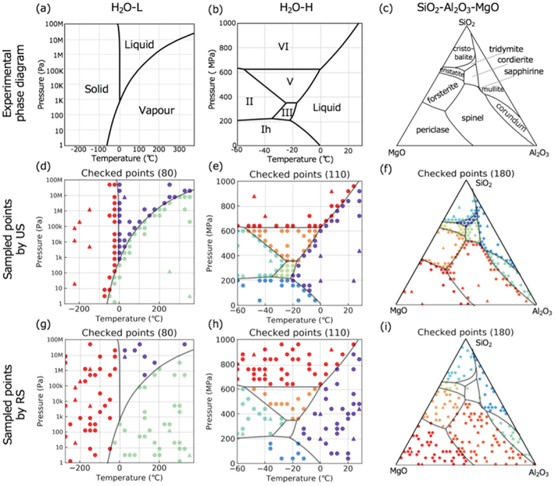
Sampling results for known phase diagrams: low pressure and high pressure phase diagrams of water, and the liquidus projection of the SiO2-Al2O3-MgO pseudo-ternary system. The top panels are the identified phase regions. The middle and bottom panels are the sampling results by the PDC algorithm and random sampling, respectively. Reprinted from ref. [107] under a creative commons attribution 4.0 international license.
Next, to verify the efficiency of the PDC algorithm for real experiments, the construction of novel phase diagrams for Zn – Sn – P film growth using molecular beam epitaxy (MBE) was performed using the PDC algorithm with LP and LC [109]. The phase diagram with varying temperatures of Sn and P evaporation sources was focused, and phase regions were identified through X-ray diffraction experiments. Starting with initial data from seven existing experimental points, the PDC algorithm suggested four additional experiments, leading to the discovery of new phase regions not identified in the initial dataset. Subsequent to this, additional seven experiments guided by PDC recommendations allowed us to construct the detail of the phase diagram [109] (see Figure 9). The phase diagram represents non-equilibrium phase regions depending on device-specific conditions, and it is difficult to predict by humans, requiring substantial effort during early-stage research. Particularly, the red regions in Figure 9 denote film deposition conditions where thin films do not grow. PDC effectively treats such conditions as distinct ‘phase regions’ enabling efficient discovery of new regions and precise determination of phase boundaries in non-equilibrium phase diagrams.
Figure 9.
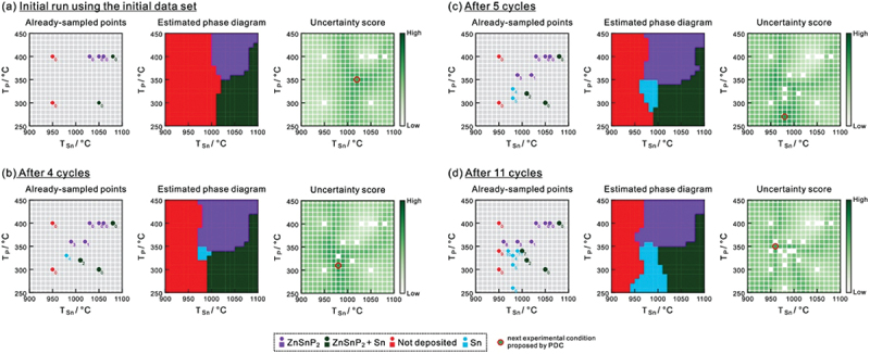
Procedures for constructing a phase diagram for the MBE growth of Zn–Sn–P films by the PDC algorithm. For each step, sampled points, an estimated phase diagram, and an uncertainty score are shown. Reprinted from ref. [109] under a Creative Commons attribution-NonCommercial license.
2.3.3. Improvements of PDC algorithm
2.3.3.1. Utilizing Gibbs' phase rule
For more effective construction of phase diagrams, two ingenuities are incorporated into the PDC algorithm: preparing training data in multiple-phase coexisting regions and reducing the search space based on the Gibbs’ phase rule [110]. The former can increase the number of training data when one experiment is performed. In addition, the latter can reduce the number of candidate experimental conditions. We demonstrated the effectiveness of our strategy by constructing ternary phase diagrams of alloy systems, incorporating these ingenuities. Even with initial knowledge limited to single-component systems, our approach significantly reduces the number of experiments required to construct a phase diagram, achieving approximately a 1/8 reduction compared to random sampling. Thus, by incorporating scientific knowledge into PDC, further acceleration can be achieved.
2.3.3.2. Treatment of high-throughput batch experiments
Recent advancements in laboratory automation and robotics enable high-throughput batch experiments. To leverage this capability, multiple experimental conditions must be selected simultaneously to effectively construct a phase diagram using machine learning techniques. We proposed strategies to select multiple conditions and compared their performance in exploring ternary isothermal sections (two-dimensional) and temperature-dependent ternary phase diagrams (three-dimensional) [111]. Our results demonstrated that even when exploring several suggestions simultaneously instead of one at a time, the overall performance does not change significantly. Therefore, we concluded that employing the PDC algorithm with multiple suggestions is suitable for high-throughput batch experiments.
2.3.3.3. Web application
Visualization is important for phase diagrams. We released the web application version of the PDC algorithm on https://aiphad.org/. The corresponding Python code is distributed as AIPHAD on https://github.com/NIMS-DA/aiphad. Using the web application, PDC can be used directly without any programming skills, and the suggestions for the next experiments, the uncertainty score mapping, and the predicted phase diagram are displayed in the browser. We have demonstrated that the phase diagrams in the Fe-Ti-Sn system exhibiting a Heusler phase can be efficiently constructed using this web application [112].
2.3.4. Phase diagram prediction by combining machine learning and the CALPHAD method
CALPHAD is the most widely used method to model and calculate phase diagrams. Combining machine learning methods and CALPHAD databases is an important future development. As a first step, we attempted to estimate unknown phase diagrams from known phase diagrams obtained by CALPHAD calculations using machine learning [113]. We focused on predicting the number of coexisting phases in each of the ten 800 K isothermal ternary sections within the Al-Cu-Mg-Si-Zn system based on the other nine sections. Using the random forest classifier, we achieved an average prediction accuracy of 84% across all ten sections, with a standard deviation of 11%. This indicates that the machine learning model can accurately predict whether a section contains single-phase, two-phase, or three-phase regions most of the time. Here, to improve prediction accuracy, we introduced new descriptors derived from the thermodynamic properties of the elements and extrapolations using the CALPHAD method. This approach is of general interest to efficiently develop new materials by predicting phase equilibria, compounds, and solid and liquid solutions in systems where phase diagrams are initially unknown. Besides, it can also be used for the initialization of PDC to select the first experiments where three-phase regions that provide a lot of information are likely to be found. This work shows that by leveraging machine learning and CALPHAD data, we can accelerate the discovery and design processes in materials science.
Phase equilibria with the liquid phase are important for the development of all kinds of materials, but currently they cannot be predicted from high-throughput experiments or simulations. Therefore, as a second step, we focused on the prediction of the liquidus [114]. We proposed a general framework for predicting binary liquidus from the properties of the pure elements and thermodynamic properties calculated using Miedema’s semi-empirical model [115]. Our framework combines three machine learning models trained and evaluated on liquidus data collected from 466 CALPHAD assessments of binary phase diagrams [114] (see Figure 10). The first model predicts the presence of liquid miscibility gaps with high accuracy (95.3%). The second and third models predict the onset temperature of solidification and the critical temperature of liquidus miscibility gaps, respectively. Using our framework, we successfully predicted the liquidus temperatures in 1563 binary systems not included in our CALPHAD dataset, many of which were previously unknown. An important feature of our models is their ability to predict the presence of eutectics. This is significant because eutectic alloys have many applications such as brazing, coolants in fast-neutron nuclear reactors, or latent thermal energy storage.
Figure 10.
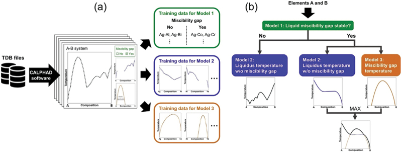
Framework for predicting binary liquidus. (a) Training data of 466 binary systems for three models. (b) Three machine learning models and procedures for predicting binary liquidus from any two elements. Reprinted from ref. [114] under a creative commons attribution 4.0 international license.
3. Experimental approaches toward the understanding, design, and exploration of new semiconductors and dielectrics
3.1. Nitride semiconductors
3.1.1. Earth-abundant nitride, Ca(Mg1−xZnx)2N2 (x = 0–1): polycrystalline bulk and epitaxial film
Recent progress in computational materials science and materials informatics is remarkably fast and leads to important predictions and subsequent experimental verification of novel (i.e. previously unknown) functional complex materials [13,116–124]. An earth-abundant ternary nitride, CaZn2N2, was proposed through computational screening using first-principles calculations as a promising optoelectronic functional nitride semiconductor with a band gap of 1.8 eV because of its small electron and hole effective masses and direct transition-type energy band structure [117]. It was also predicted that the band gap could be widely tuned from the ultraviolet region to the red – infrared one by simple element-substitutions such as Mg or Cd substitution at the Zn site and Sr substitution at the Ca site [117,122], suggesting that this nitride would be a promising host candidate of a light-emitting semiconductor and/or a photovoltaic semiconductor devices with appropriately tuned band gaps.
Based on the prediction, polycrystalline samples of Ca(Mg1−xZnx)2N2 (x = 0–1) were successfully synthesized via a solid-state reaction using binary nitride precursors at ambient pressure or an extremely high pressure (5 GPa) [125]. It is experimentally validated that the optical band gap can be continuously tuned from 3.2 eV to 1.8 eV (i.e. the ultraviolet-to-red region) and the corresponding band-to-band photoluminescence (PL) is observed even at room temperature [125] (Figure 11(a)). In the entire x range, the observed band gaps are close to those predicted by first-principles calculations [117,125] (Figure 11(b)). Additionally, heteroepitaxial growth of a CaZn2N2 (i.e. x = 1) thin film was demonstrated by MBE with precise optimization of growth conditions [126] (Figure 11(c,d)). Three key factors for heteroepitaxy were found: (i) the precise tuning of the individual flux rate of Knudsen cells for Ca and Zn, (ii) the use of GaN template layer on c-plane sapphire as a substrate, and (iii) the application of MBE with an active nitrogen radical source because other attempts at physical vapor deposition and thermal annealing processes did not produce pure CaZn2N2 films. Since the GaN template layer exhibits non-negligible n-type conduction, reliable carrier transport measurement was difficult. Thus, the electronic transport properties of CaZn2N2 films deposited on a yttria-stabilized zirconia (YSZ) single-crystal and a silica glass were evaluated by Hall-effect measurements at room temperature. It was clarified that the dominant carrier types were p- (holes) and n-type (electrons) for the films on YSZ and silica glass, respectively. This ambipolar carrier-doped state was unintentionally formed, while would be an advantageous dopability to fabricate a pn homojunction. The estimated carrier densities of both the films were as low as 1013 cm−3 order, which implies that CaZn2N2 has potential for controlling carriers over a wide range from intrinsic (i.e. close to insulating), semiconducting, through to degenerate states by impurity doping. Despite the theoretically predicted small effective masses [117], the carrier mobilities were as low as 0.3 cm2/(V·s) for holes (YSZ) and 4.3 cm2/(V·s) for electrons (silica glass) due probably to the poor crystallinity of the films. These studies on polycrystalline bulks and epitaxial films experimentally clarified that the earth-abundant nitride, Ca(Mg1−xZnx)2N2 (x = 0–1), can be a promising semiconductor material that plays an emitting layer in a wide-range wavelength-tunable light-emitting diode or a light absorber layer in a photovoltaic cell. However, to achieve superior carrier transport, different nitridization processes must be essential to overcome a dilemma; i.e, high nitrogen chemical potential requires low substrate temperature, but high crystallinity usually does high substrate temperature.
Figure 11.
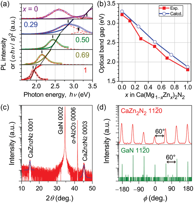
Optical and structural characteristics of Ca(Mg1−xZnx)2N2. (a) Photoluminescence (PL) and absorption (αhν/s)2 spectra of polycrystalline samples at room temperature. (b) Optical band gaps (Exp.) estimated from (a). The calculated ones (Calcd.) are shown for comparison. (c, d) X-ray diffraction profiles of an epitaxial CaZn2N2 (i.e. x = 1) thin film with ~50 nm thickness, optimally grown by MBE, on a GaN template layer on c-plane sapphire substrate. (c) Out-of-plane 2θ scan. (d) In-plane scan. Adapted with permission from refs. [125,126]. Copyright 2019 American chemical society.
Similar to the discovery of CaZn2N2 by computational screening [117], the exploration of new functional ternary nitrides has been actively performed by considering thermodynamic stability/metastability and predicting functionality [118,120,127]. Even though nitrides particularly remain unexplored mainly due to difficulty in synthesis, it has recently become to overcome the difficulty owing to advancing various synthetic techniques [128]. A representative demonstration would be a successful synthesis of new ternary perovskite-type nitrides and II-IV-N2 type ones. Although nitride perovskites, excluding TaThN3 [129] and anti-perovskite-type nitrides [130], had not been reported due to the synthesis difficulty, first-principles studies have proposed unreported but thermodynamically stable perovskite-type nitrides as well as their electronic structures [131]. After that, among the predicted ternary nitrides, LaReN3 (in 2021) [132] and LaWN3 (in 2021–2023) [133–136] have been experimentally synthesized. Recently, novel ternary II-IV-N2 compounds such as AeTmN2 (Ae = Ca, Sr, Ba; Tm = Ti, Zr, Hf) [137,138] have also been successfully synthesized. Therefore, a large research platform on ternary nitrides may be about to expand more actively and rapidly.
3.1.2. Thin-film growth of perovskite-type LaWN3: toward ferroelectric semiconductor applications
Ferroelectric photovoltaic cells are expected to offer highly efficient electric power generation owing to their extremely high operating voltages [3]. The ferroelectric photovoltaic effect has been examined mainly in perovskite-type oxides such as BiFeO3. However, the conversion efficiency of ferroelectric photovoltaic cells based on the related oxides remains low (~8%) [139]. One of the origins seems to be its low sunlight absorption efficiency originating from the wide band gap of ~2.7 eV for BiFeO3 [140].
Under such a circumstance, a perovskite-type nitride, LaWN3, has been expected to have potential as a rare and new ferroelectric semiconductor because it is predicted to exhibit ferroelectricity with a high spontaneous polarization of ~ 60 μC/cm2 [141] and have a narrower band gap of approximately 1.6 − 1.8 eV according to first-principles calculations [134,142]. These characteristics may make it more suitable for applications as the light-absorbing layer of ferroelectric photovoltaic cells than the perovskite-type oxides. However, the ferroelectric properties of LaWN3 have yet to be experimentally confirmed: only a piezoelectric response was reported for a sample synthesized [133]. In addition, the LaWN3 samples reported so far are crystallographically non-oriented polycrystalline [133,134], which hinders the predicted ferroelectric polarization. Thus, it was strongly required to fabricate a highly oriented epitaxial film, especially the c-axis, which is a polar direction of LaWN3 with a rhombohedral R3c space group.
LaWN3 epitaxial films with ~65 nm thickness were grown on c-plane α-Al2O3 substrates with the multi-cathode rf magnetron sputtering guns and nitrogen gas [135]. A substrate temperature (Ts) higher than 1000°C and optimization of rf power densities of the La and W cathodes were essential for heteroepitaxial growth (Figure 12(a)). The heteroepitaxial relationship between the film and the substrate is LaWN3 [0001] || α-Al2O3 [0001] for out-of-plane and LaWN3 [100] || α-Al2O3 [110] for the in-plane; i.e. c-axis of LaWN3 is oriented perpendicular to the c-plane of α-Al2O3 substrate and the in-plane domain of LaWN3 is rotated by 30° with respect to that of α-Al2O3 (Figure 12(b)). Electronic transport measurements for the obtained epitaxial film revealed that the film exhibited no temperature dependence of n-type electrical conductivity (σ) (i.e. a heavily electron-doped degenerate semiconductor) (Figure 12(c)). Because the carrier density was as high as 2 × 1022 cm−3 and the corresponding sample resistance was too low (<1 kΩ), the predicted ferroelectricity was not observed as also reported in Ref. [133]. Optical measurements indicated that the high-density carriers induced free carrier absorption over near-infrared wavelengths and widened the optical band gap to 1.83 eV owing to the band-filling effect (Figure 12(d)). Moreover, the film exhibited superconductivity at 0.7 K (inset of Figure 12(c)). The degenerate state and superconductivity are attributed to the high-density electron carriers that resulted from the unavoidable off-stoichiometry (excess of W and/or N deficiency) to achieve heteroepitaxial growth.
Figure 12.
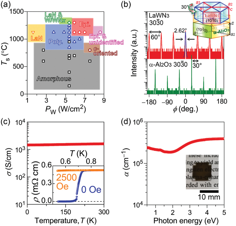
Heteroepitaxial growth and optoelectronic properties of perovskite-type LaWN3 thin films. (a) Optimization of film-growth conditions: Ts and PW denote substrate temperature and rf power density of a tungsten cathode, respectively. The optimum region for epitaxial growth is indicated by red. (b) Epitaxial relationship of the optimally grown film. (c) Temperature dependence of the electrical conductivity (σ) of the epitaxial film. The inset shows resistivity (ρ = 1/σ) in an extremely low temperature region of ≤0.9 K under external magnetic fields. (d) The optical absorption coefficient (α) spectrum of the epitaxial film. The inset is a sample picture. Adapted with permission from ref. [135]. Copyright 2023 American chemical society.
Reports on successful synthesis of LaWN3 samples are still scarce because extremely high external pressure or precise control of film-growth conditions is necessary for polycrystal powders [134,136] or for thin films [133,135], respectively. However, fundamental researches on LaWN3 have been gradually progressing. A recent research on neutron diffraction reveals that the nitrogen vacancy stabilizes an orthorhombic structure, not rhombohedral R3c, with a polar symmetry (Pna21) that possesses a unique atomic polarization along the c-axis [136]. Additionally, a recent research on thin films clarifies that the electrical resistivity of LaWN3 is quite sensitive to La/(W+La) in the films (i.e. cation ratio) [143]. Thus, different growth processes that realize a higher nitrogen chemical potential will be required to achieve a stoichiometric chemical composition for the realization of lower carrier density and observation of the predicted ferroelectricity. Because this perspective is almost the same as the case of CaZn2N2 in the former section, the development of a new active nitrogen source apparatus alongside a new concept would be a critical issue to advance research on these nitride semiconductors.
3.2. Phosphide semiconductors for photovoltaic applications
Recently, some novel semiconductors for photovoltaics have been investigated with the aid of theoretical calculations and/or machine learning. We focused on ternary zinc phosphides because they have suitable electronic structures and phosphorus vacancies are less likely to form mid-gap states considering the behavior reported for the binary zinc phosphide [144]. In particular, ZnSnP2 (ZTP) with a chalcopyrite structure is an emerging absorber in view of its light-absorption and electric characteristics. To achieve higher energy conversion efficiency in ZTP solar cells, the suppression of the recombination of photo-generated carriers is a key issue. Point defects in bulk regions and heterointerfaces in devices can be sites of carrier recombination. Therefore, we explored ways to understand and improve the carrier recombination properties through a combination of experimental and theoretical studies as described below. In addition, new materials for photovoltaic applications were investigated.
3.2.1. Evaluation and control of native point defects in phosphide semiconductors
Identifying deep and shallow levels in ZTP is the first step to understand the carrier recombination properties in absorber materials. Deep level transient spectroscopy (DLTS) is well known to be a technique to detect trap levels in semiconductors and has also been applied to recent state-of-the-art devices. A discussion based on the formation energies and energy levels of point defects derived from first-principles calculations is fruitful for conventional materials of thin-film solar cells and even for emerging absorber materials. Actually, it was clearly shown for some absorber semiconductors that emissions observed in PL spectra consist of some recombination processes related to shallow and deep levels. In this study, ZTP bulk crystals obtained by a conventional solution growth were characterized by DLTS and photoluminescence (PL) for discussion on levels related to point defects in conjunction with the results of first-principles calculations by Kumagai et al. [145].
A conventional DLTS measurement and theoretical calculations revealed two shallow trap levels coming from antisite defects and a deep trap state [146], but detailed properties were still unknown. Therefore, advanced DLTS and minority carrier transient spectroscopy (MCTS) using the correlation function method were carried out in cooperation with Ceramicforum Co. Ltd. [147]. Figure 13(a) shows the Arrhenius plot for the time constant t of hole or electron emission obtained from DLTS and MCTS spectra, and five (H1–H5) and two (E1, E2) traps were evaluated for hole and electron, respectively [147]. The capture cross section and the activation energy corresponding to a trap level can be evaluated by analyzing the plot based on the Shockley – Read – Hall model, and the trap density was obtained from the capacitance measurements. The trap density is in the range of 1014–1015 cm−3 in all traps, whereas the capture cross section of trap E1 is 4.0 × 10⁻¹¹ cm−2 which is 2–5 orders of magnitude larger than others, resulting in the much shorter time constant. This means that trap E1 might have a dominant contribution to the capture of electrons from the CBM. The theoretical calculations suggest that trap E1 originates from the Sn antisite defect on the Zn site, SnZn in the viewpoints of the activation energy and thermodynamic transition level.
Figure 13.

(a) Arrhenius plot of time constant from DLTS and MCTS. (b) TRPL spectra of ZTP crystals. (c) Chemical potentials of Zn, Sn, and P in equilibrium of ZTP and liquid solution. Reproduced from ref. [147] with the permission of AIP publishing.
Next, we attempted to suppress the formation of SnZn antisites by controlling the chemical potentials during crystal growth. According to the theoretical calculations, the formation energy of SnZn is higher under the conditions of higher chemical potential of Zn. Conventionally, ZTP crystals were prepared with the composition of the Sn-ZTP pseudo-binary system. We prepared crystals with various initial compositions such as Zn-rich, P-rich, and Sn,P-rich in addition to the conventional composition. Time-resolved photoluminescence (TRPL) spectra of ZTP crystals shown in Figure 13(b) revealed that the TRPL lifetime is longer for crystals in the Zn-rich condition, which is consistent with the decrease in the concentration of SnZn [147]. However, the actual defect formation behavior depends on the chemical potentials of constituent elements, and then they were evaluated using a sub-regular solution model under the condition in equilibrium ZTP solid and liquid solution, in other words, precipitation from liquid. Figure 13(c) clarifies that the chemical potential of Zn in the Zn-rich condition is higher than those in other conditions and suggests the suppression of the Sn antisite formation [147].
As seen in the above, a fusion of experiments and calculations is effective in the discussion of defect formation based on chemical potentials. It is desired that a more quantitative discussion will be developed in the future.
3.2.2. Interfaces for phosphide solar cells
In thin-film solar cells with compound semiconductors, there are some heterointerfaces because of the multilayer structure with various materials. As mentioned above, interfaces can be carrier recombination sites and the effect appears in the resistance. Since ZTP is an emerging absorber, every interface should be examined and controlled in addition to the pn junction. We first focused on the interface between the ZTP absorber and the back electrode.
In solar cells consisting of sulfide or selenide absorbers, Mo is conventionally used as a back electrode to obtain ohmic contact. However, our previous work clarified that the series resistance of ZTP solar cells could be reduced by applying Cu to the electrode rather than Mo [148]. The Cu/ZTP interfacial structure and its impact on carrier transport behavior are discussed here. Annealing experiments of Cu-deposited ZTP crystals revealed the formation of a copper phosphide, Cu3P, at the interface, leading to the reduction of the resistance. In this case, selected area electron diffraction (SAED) suggested Cu3P epitaxially formed on ZTP crystals with the relationship of Cu3P[1100](0001)//ZTP [110](112). Additionally, it was revealed that the IP of ZTP and the work function of Cu3P are comparable by photoelectron yield spectroscopy (PYS). These results indicate that the heterostructure with lattice-matched and band-aligned is required for the suppression of carrier recombination at interfaces. This interface structure was applied to solar cells. In particular, the insertion of Cu3P before annealing enhanced the solar cell performance, as shown in Figure 14, and consequently, the best energy conversion efficiency of 3.87% was achieved [149].
Figure 14.
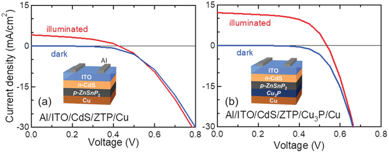
Current density-voltage characteristics of ZTP solar cells (a) without and (b) with insertion of Cu3P. Created based on ref. [149]. Copyright 2020 Elsevier B.V. All rights reversed.
Next, turning to the pn junction, an n-CdS/p-ZTP structure was adopted in the solar cell with the best efficiency. CdS is a conventional n-type layer for compound thin-film solar cells, but the large CBM offset at the n-CdS/p-ZTP interface was suggested by X-ray photoelectron spectroscopy (XPS) [150]. Considering the discussion on the Cu3P/ZTP interface, CdSnP2 (CTP) is a candidate as an n-type partner with ZTP. The crystal structure of CTP is also chalcopyrite and the first-principles calculations suggest a smaller CBM offset in the n-CTP/p-ZTP junction compared to CdS/ZTP [151]. Samples including a CTP/ZTP interface were prepared by phosphidation of Cd-Sn precursor films on ZTP crystals [152,153] and the current-voltage curve was measured. The epitaxial relationship between the deposited CTP and ZTP crystals is clearly confirmed from the scanning transmission electron microscope (STEM) dark-field (DF) image and SAED patterns in Figure 15 and a good rectification was obtained in the n-CTP/p-ZTP junction [153]. A higher performance of ZTP solar cells is expected by adopting this junction. Our work means that the research assisted by theoretical calculations is also effective in the interface design in devices.
Figure 15.
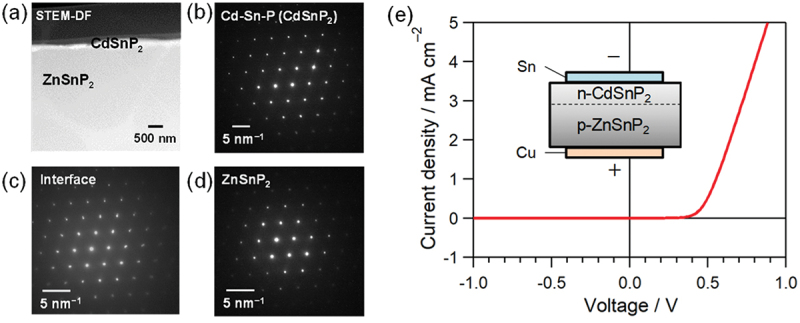
(a) STEM-DF image of CTP/ZTP interface and corresponding SAED patterns of (b) CTP, (c) interface, and (d) ZTP regions. (e) Current density-voltage curve for n-CTP/p-ZTP junction. Reproduced from ref. [153] with permission. Copyright IOP publishing. All rights reserved.
3.2.3. Novel materials for photovoltaic applications
We also tried to develop novel materials with the assistance of theoretical calculations. Among ternary compounds containing Zn and P, compounds including alkaline earth elements were suggested for potential photovoltaic applications from the viewpoints of semiconductor properties such as the band gap and effective mass.
For X-Zn-P compounds (X: group II elements), we investigated MgZn2P2 formed at the Mg/Zn3P2 junctions in Zn3P2-based solar cells. The detailed nature of this device had been controversial for a long period, but we have recently revealed that this is a heterojunction of semiconductors between Zn3P2 and Mg(MgxZn1−x)2P2 formed through the reaction at the Mg/Zn3P2 interface [154]. The lattice mismatch between Mg(MgxZn1−x)2P2 and Zn3P2 is 0.5% at most and, thus, is favorable for carrier transport. Mg(MgxZn1−x)2P2 can be regarded as a solid solution of MgZn2P2. Therefore, our work provided the preparation of MgZn2P2 although there was no report on its synthesis. Theoretical calculations have suggested that the stable crystal structure of Mg(MgxZn1−x)2P2 is the trigonal CaAl2Si2-type shown in Figure 16(a). Inspired by this compound, we focused on a series of compounds, CaZn2P2 (CZP), SrZn2P2 (SZP), and BaZn2P2 (BZP), which are classified as Zintl compounds and still in an undeveloped group. A synthesis route using Sn solution as a solvent was adopted to suppress the reactivity of group II elements. Figure 16(b) shows XRD profiles of samples after the heat treatment to obtain compounds [155]. The trigonal CaAl2Si2-type phases were identified in the profiles of CZP and SZP although they include diffractions from Sn and secondary phases, while the profile for BZP was assigned to a tetragonal ThCr2Si2-type structure. The unidentified phase was observed in the CZP-Sn sample, but it might be the products by the decomposition of calcium phosphides and not affect the later evaluation of optoelectronic properties. The UV-vis diffuse reflectance analyses evaluated the indirect (1.7–1.85 eV) and direct band gaps (1.9–2.05 eV) for CZP and SZP, whereas it was difficult to evaluate for BZP because its band gap may be much narrower. The theoretical calculations also confirmed the crystal structures and the trend that their direct band gaps are slightly larger than the indirect band gaps.
Figure 16.

(a) Structure of Mg(MgxZn1−x)2P2 (trigonal CaAl2Si2-type). (b) XRD profiles for CaZn2P2, SrZn2P2, and BaZn2P2. (c) Relationship between the nearest-neighbor pnictogen–pnictogen distance and fundamental band gap for pnictide semiconductors. Reprinted with permission from ref. [154]. Copyright 2018 American chemical society and from ref. [155] under a creative commons attribution 4.0 international license.
The evaluated direct band gaps for CZP and SZP are somewhat too large for application to absorbers, but they can be applied to buffer layers like Mg(MgxZn1−x)2P2 in Zn3P2 solar cells. PYS measurements provided that the IPs for CZP and SZP are similar to those of ZTP and Zn3P2, leading to their small CBM offset within 0.2 eV. On the other hand, Figure 16(c) summarizes the relationship between fundamental band gap and nearest neighbor pnictogen – pnictogen distance, which is an index for lattice-matching, for various pnictide semiconductors. The dotted lines indicate the range of 1% lattice mismatching with ZTP and Zn3P2, and especially it is found that CZP is well-matched with phosphide absorbers. Consequently, CTP would be an appropriate partner material in Zn3P2- and ZTP-based solar cells from the viewpoints of lattice and band matching.
In previous works, the calculation-assisted developments of materials for photovoltaic applications are focused mostly on absorbers. However, lack of investigation of n-type buffer materials also limits the development of novel solar cells. This work indeed suggests that the investigation of such materials would be required.
3.3. Layered perovskite dielectrics
Ferroelectric oxides are fascinating targets for the exploration of functional materials due to their diverse properties, which make them valuable for various applications such as non-volatile memories and high-performance piezoceramics. Traditionally, ferroelectric oxides have been developed in perovskite-type compounds with the composition ABO3, exemplified by BaTiO3 and Pb(Zr,Ti)O3 (PZT). Extensive experimental and theoretical studies have established several guiding principles for designing ferroelectric perovskite-type compounds. These principles include the second-order Jahn-Teller (SOJT) effect [156–162], the tolerance factor [163], and the stereochemical activity of lone-pair electrons [164,165].
The field of exploration for ferroelectric materials is expanding beyond perovskite-type compounds to include non-perovskite types such as fluorite-type [166–169], layered-silicate-type [170–172], and aluminate-sodalite-type compounds [173–175]. Moreover, the concept of hybrid improper ferroelectricity (HIF) has recently inspired renewed interest in layered-perovskite-type compounds [176–180]. HIF can be understood as ferroelectricity induced by a special combination of lattice instabilities at finite wave vectors [177]. Specifically, in layered perovskite-type compounds, the rotation of corner-shared oxygen octahedra contributes to the emergence of ferroelectricity [179,181–184]. This contradicts the conventional understanding that non-polar lattice vibrations do not result in spontaneous polarization when they freeze. This discovery has underscored the significance of octahedral rotation in the design of ferroelectric materials within layered-perovskite-type compounds.
There are three typical structures in layered perovskite-type compounds: Aurivillius-type, Dion-Jacobson-type (DJ-type), and Ruddlesden-Popper-type (RP-type) phases. Li2SrNb2O7 crystallizes in a similar structure but slightly different from the RP-type. As shown in Figure 17, an ‘n = 2’ RP-type structure of Ca3Mn2O7 consists of perovskite-type building blocks and rocksalt-type CaO layers, which stack along the [001] direction. In the pseudo-RP-type structure of Li2SrNb2O7, however, Li2O layers are inserted instead of rocksalt-type layers, reducing the distance between perovskite-type building blocks. This section presents our finding that the close competition between the SOJT effect and the octahedral rotation in Li2SrNb2O7 creates a fertile ground for designing various dielectric properties, including ferroelectricity and also antiferroelectricity [185–188].
Figure 17.
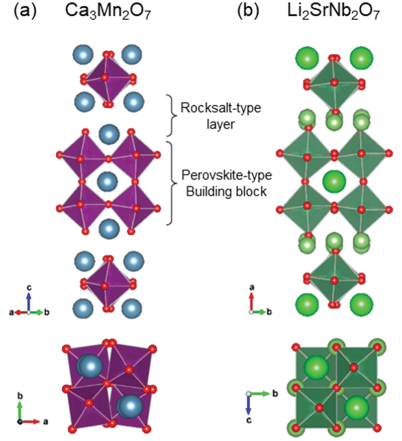
Crystal structures of (a) ruddlesden-popper and (b) pseudo-ruddlesden-popper phases. Adapted with permission from ref. [185]. Copyright 2019 American chemical society.
Figure 18(a) presents the temperature dependence of complex dielectric permittivity for a Li2SrNb2O7 polycrystalline sample over a temperature range from 4.2 K to 300 K [185]. The top and bottom panels show the real (ϵ’) and imaginary (ϵ’’) parts, respectively. As shown in the figure, ϵ’ increases upon cooling from 300 K, reaching a maximum value of approximately 210 around 220 K. Upon further cooling, it decreases, exhibiting a cusp-like anomaly that indicates a phase transition. A corresponding anomaly in ϵ’’ is also observed around 220 K. The inset in the top panel, which magnifies the temperature region where the anomaly occurs, shows slight differences between the results measured during cooling and heating, suggesting a weak first-order phase transition.
Figure 18.
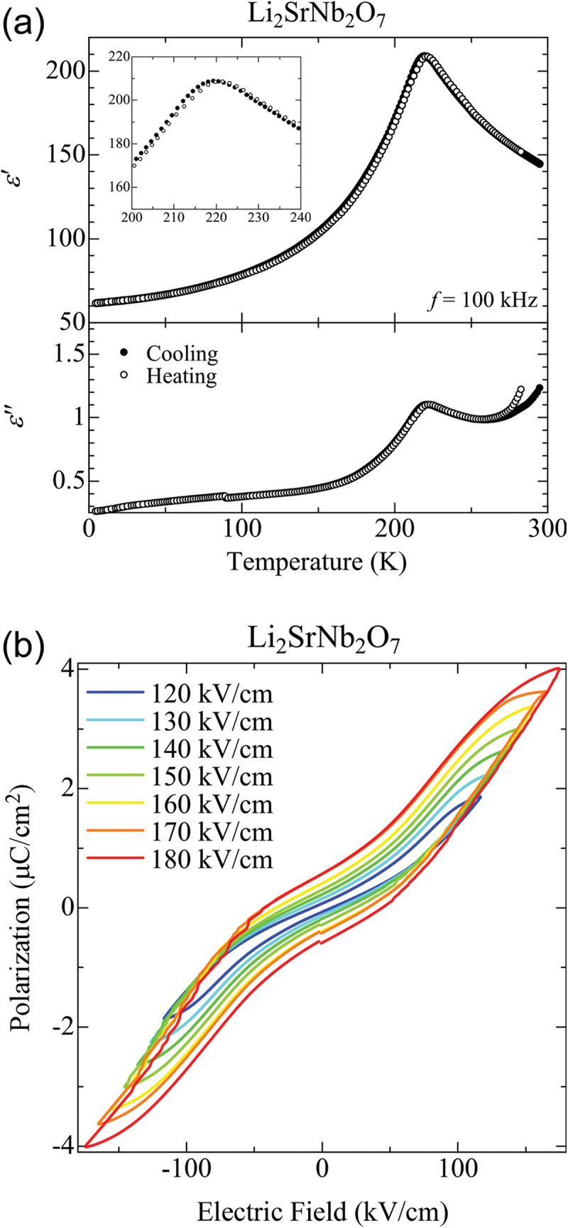
(a) Temperature dependences of the real and imaginary parts of the complex (relative) permittivity of Li2SrNb2O7, measured at a frequency of 100 kHz. (b) p–E hysteresis loops of Li2SrNb2O7, measured at a frequency of 10 hz at 80 K. Adapted with permission from ref. [185]. Copyright 2019 American chemical society.
Figure 18(b) plots the electric-field-induced polarization of Li2SrNb2O7 under various maximum applied electric fields [185]. When an electric field of 120 kV is applied, a slim but clear double hysteresis loop appears, demonstrating the antiferroelectric property of Li2SrNb2O7. Notably, a weak polarization remains at zero electric field and gradually increases as the applied electric field rises. Since the polarization measurement was performed at 80 K, where the sample exhibits sufficiently high insulating properties, the influence of leakage current can be ruled out. This result suggests that a ferroelectric component coexists in Li2SrNb2O7.
Synchrotron X-ray diffraction measurements of Li2SrNb2O7 have clarified appearance of superlattice reflections in the low-temperature region (Figure 19(a,b)), indicating that the structural phase transition between Cmcm and P21cn symmetries occurs around 220 K during cooling [185]. The polar structure of P21cn in the low-temperature phase is consistent with the presence of remanent polarization at zero electric field. As presented in Figure 19(c–f), structural analyses reveal that the P21cn structure of Li2SrNb2O7 consists of in-plane antipolar displacements and out-of-plane polar displacements of Nb atoms along the [001] and [100] directions, respectively, indicating the coexistence of antiferroelectricity and ferroelectricity in the system [185]. In the high-temperature Cmcm phase, the Sr and Nb atoms are located on a mirror plane normal to the [001] direction. In the low-temperature P21cn phase, on the other hand, the mirror plane disappears due to the relative displacements of the Sr and Nb atoms along the [001] direction, inducing a local electric dipole moment within the perovskite-type block. While all local dipoles are parallel within the perovskite-type building block, they align antiparallel between adjacent building blocks, forming an antipolar configuration along the [001] direction. Furthermore, the local dipoles slightly tilt to the [100] direction, which cooperatively generates the spontaneous polarization.
Figure 19.
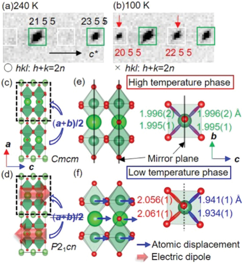
X-ray diffraction patterns of Li2SrNb2O7 observed at (a) 240 K and (b) 100 K. The crystal structures in the high- and low-temperature phases are illustrated in panels (c) and (e) and panels (d) and (f), respectively. Adapted with permission from ref. [185]. Copyright 2019 American chemical society.
First-principles calculations play a key role in elucidating the driving force behind the long-range ordering of local dipoles. Figure 20 presents the phonon dispersion curves of Li2SrNb2O7 calculated for the Cmcm (top panel) and P21cn (bottom panel) structures [185]. Data points plotted below the origin of the vertical axis in the top panel indicate an imaginary frequency, where the corresponding oscillation is unstable in the given symmetry. As shown in the top panel, there are two imaginary frequency modes at the Γ and Y points in the high-temperature Cmcm phase. These modes are known as ‘soft modes’, and their freezing induces a displacive-type phase transition. In a second-order phase transition, the displacement pattern of the soft mode corresponds to the change in crystal structure through the transition. Although Li2SrNb2O7 undergoes a first-order phase transition, as mentioned earlier, the displacement pattern of the soft mode provides insight into the mechanism of the phase transition due to its sufficiently weak first-order nature manifested by the subtle thermal hysteresis in the temperature dependence of the dielectric permittivity. Our first-principles calculations clarified that the most unstable phonon mode is at the Γ point [187]. When the Γ2− soft mode freezes, a polar structure of Cmc21 is generated, as shown in Figure 21(b), where spontaneous polarization appears along the [001] direction. However, the Cmc21 structure is found to be incompatible with the structure determined experimentally by structural analyses. On the other hand, the freezing of the Y2− soft mode results in a Pmcn structure. Although this Pmcn structure is non-polar, it exhibits antipolar ordering of the Nb displacements along the [001] direction, which aligns with the results of the structural analyses. Therefore, it is reasonable to attribute the origin of the long-range ordering of local dipoles to freezing of the Y2− soft mode, despite it being slightly less imaginary than the Γ2− soft mode, likely due to the accuracy of the calculation. The bottom panel in Figure 20 shows the phonon dispersion curves of Li2SrNb2O7 with the P21cn structure [185]. There is no soft mode in the system, confirming that the P21cn structure is the ground state of Li2SrNb2O7, from a computational perspective as well.
Figure 20.
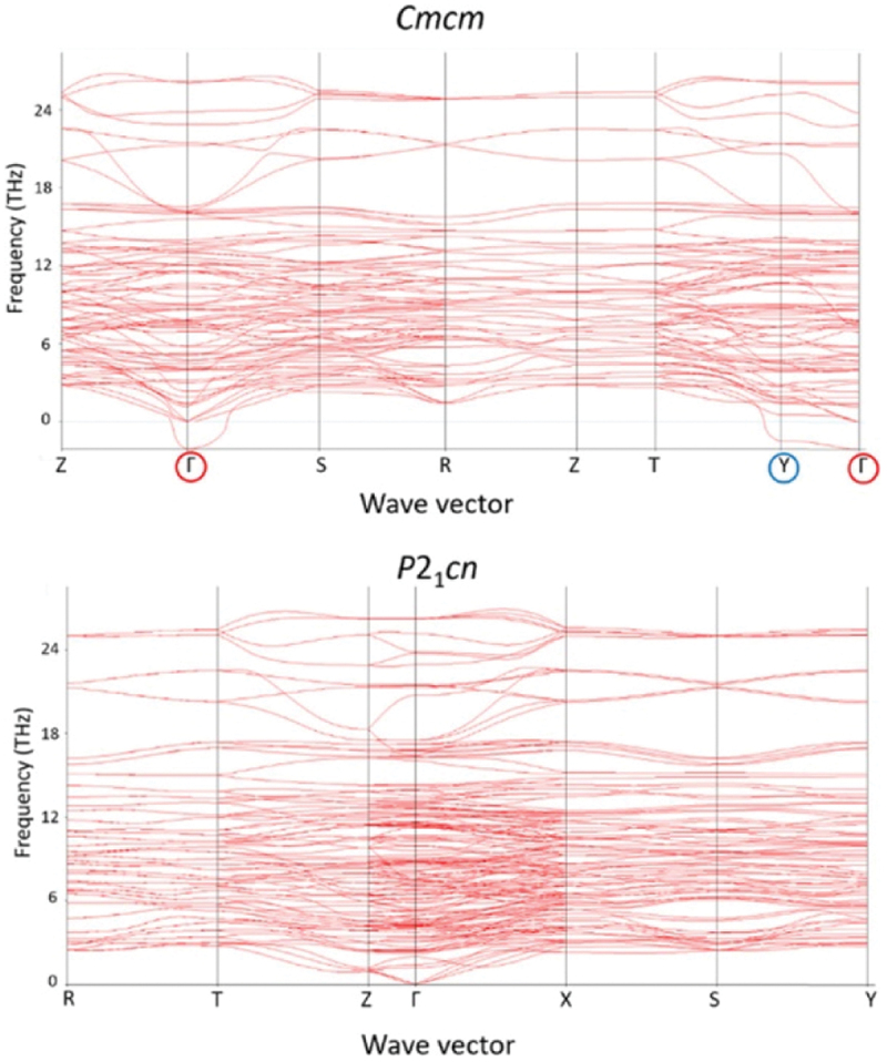
Calculated phonon bands of Li2SrNb2O7 in the paraelectric Cmcm phase (top) and the weak-ferroelectric P21cn phase (bottom). The reciprocal points Γ and Y with softmodes are indicated in red and blue circles, respectively. Adapted with permission from ref. [185]. Copyright 2019 American chemical society.
Figure 21.
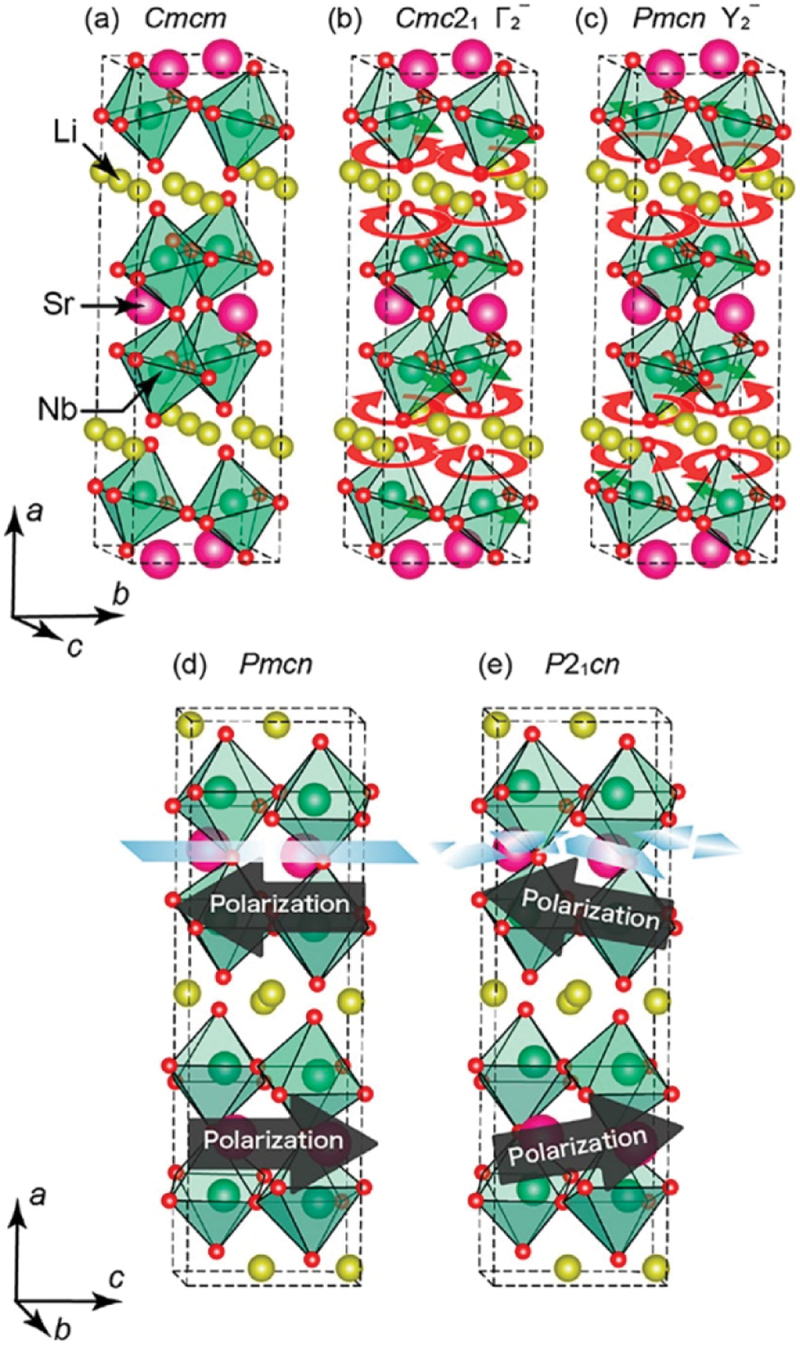
Crystal structures of Li2SrNb2O7: (a) in the paraelectric Cmcm phase, and (b, c) the phonon modes transforming as irreducible representations (b) Γ2– and (c) Y2–, leading to the Cmc21 and pmcn phases, respectively. Schematics of (d) the antiferroelectric pmcn and (e) weak ferroelectric P21cn phases. The mirror symmetry perpendicular to the a axis is preserved in the pmcn phase, whereas it is broken in the P21cn phase. Adapted with permission from ref. [187]. Copyright 2021 American chemical society.
The displacement pattern of the Y2− soft mode consists of the relative displacement of Nb and the rotation of oxygen atoms, as shown in Figure 21(d). The origin of the Nb displacement can be understood within the framework of the SOJT effect, as visualized in Figure 22. Figure 22 shows the crystal orbital Hamilton population (COHP) [189–193] and schematics of energy-level diagrams calculated for Li2SrNb2O7 in Cmcm and Pmcn symmetries [186]. The horizontal axis in panels (a) and (b) represents negative COHP (−COHP), with positive and negative values indicating bonding and antibonding states, respectively. As indicated by the arrow in panel (b), the bonding interaction between Nb 4d and O 2p orbitals is enhanced during the transformation from the Cmcm structure to the Pmcn structure due to the freezing of the Y2− soft mode, demonstrating that the Nb atom is attracted toward the ligand oxygen due to the SOJT effect. Panels (e-h) in Figure 22, on the other hand, present COHP and energy-level diagrams for Li2SrTa2O7. In marked contrast to Li2SrNb2O7, the COHPs for the Cmcm and Pmcn structures overlap each other, indicating that the enhancement of the bonding interaction due to the transformation to the Pmcn structure is absent. This result shows that the SOJT effect is suppressed by substituting Nb with Ta. Figure 23 shows the temperature dependence of the dielectric permittivity in Li2Sr(Nb1-xTax)2O7 with varying Ta content x [186]. As shown in the figure, the cusp anomaly due to the phase transition shifts to lower temperatures as x increases, demonstrating that Ta substitution suppresses the emergence of the low-temperature structure. The variation of the phase transition temperature (Tc), plotted as a function of x in panel (b), shows that the phase transition disappears for x greater than 0.4. It would thus be reasonable to conclude that the phase transition of Li2SrNb2O7 is driven by the SOJT effect between the Nb and ligand O atoms.
Figure 22.
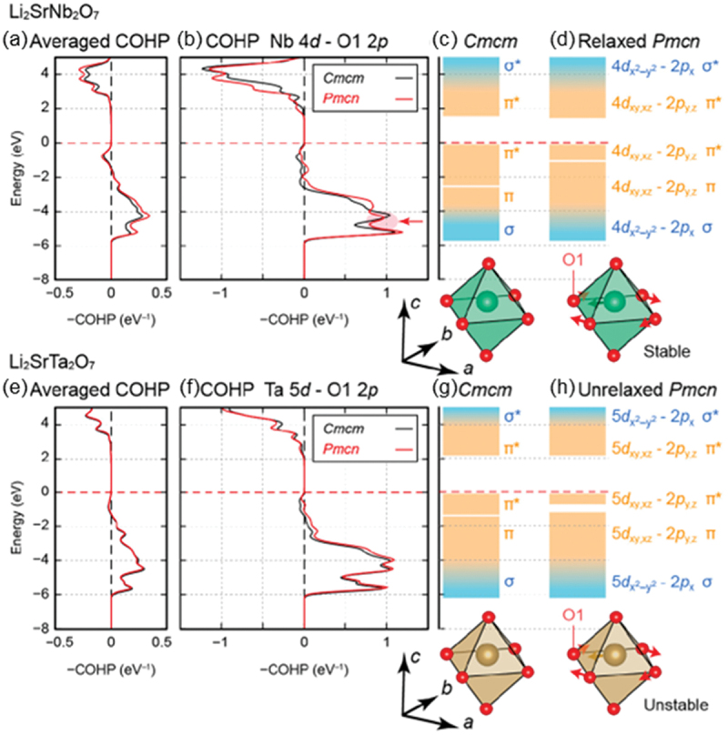
Averaged negative-signed COHPs in (a) Li2SrNb2O7 and (e) Li2SrTa2O7 for all atom pairs with bond lengths less than 3 Å. (b) Negative-signed COHPs between Nb 4d and O 2p states for Li2SrNb2O7 and (f) those between Ta 5d and O 2p states for Li2SrTa2O7 in the cmcm and pmcn phases. Schematic energy level diagrams for the (c) cmcm and (d) pmcn phases of Li2SrNb2O7 as well as the (g) cmcm and (h) pmcn phases of Li2SrTa2O7 are described. Adapted with permission from ref. [186]. Copyright 2020 American chemical society.
Figure 23.
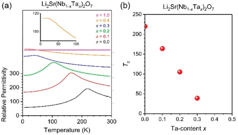
(a) Temperature dependences of relative dielectric permittivity in Li2Sr(Nb1–xTax)2O7 with various x, which were measured at 100 kHz. The inset indicates a magnified view focused on the low-temperature range in the case of x = 0.4. (b) Ta-content dependence of ferroelectric phase transition temperatures in Li2Sr(Nb1–xTax)2O7. Adapted with permission from ref. [186]. Copyright 2020 American chemical society.
As shown in Figure 21(c), the Y2− soft mode includes not only the Nb displacements but also the rotational distortions of oxygen octahedra around the principal axis of the crystal. Similar to the case of Ca3Mn2O7, the Cmcm phase of Li2SrNb2O7 originally contains the tilting distortions around the axis perpendicular to the [100] axis (see Figure 21(c)). Therefore, the rotational distortions of octahedra would activate HIF through its combination with the tilting rotations, in analogy with ‘n = 2’ RP-type oxides such as Ca3Mn2O7. To clarify this hypothesis, phase instability was examined in Li2(Sr1-xCax)Nb2O7. According to the concept of the tolerance factor for the perovskite-type structural unit, a reduction in the size of the A-site cation enhances the magnitude of the octahedral rotation. Therefore, substituting Ca for Sr provides a good test for the role of HIF in the ferroelectricity of Li2(Sr1-xCax)Nb2O7, since Ca has a Shannon ionic radius of 1.00 Å in six coordination, which is smaller than 1.18 Å for Sr. Figure 24 presents the electric-field-induced polarization measured in Li2(Sr1-xCax)Nb2O7 with compositions of x = 0 and 0.1 [187]. As shown in the figure, the remanent polarization increases with Ca substitution. This result strongly supports the hypothesis that HIF also contributes to the ferroelectricity in Li2SrNb2O7.
Figure 24.
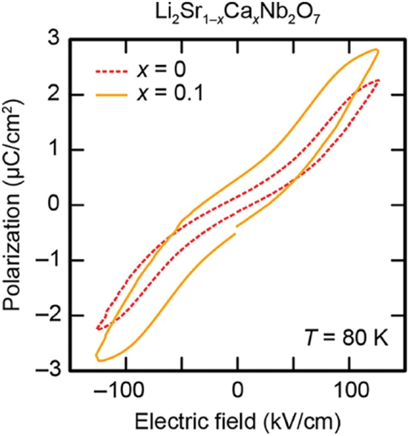
p–E hysteresis loops of Li2SrNb2O7 (red dashed line) and Li2Sr0.9Ca0.1Nb2O7 (orange solid line), measured at a test frequency of 10 Hz and a temperature of 80 K under an applied electric field of 130 kV/cm. Adapted with permission from ref. [187]. Copyright 2021 American chemical society.
The HIF also plays a role in the onset of the phase transition, in addition to the SOJT effect, by stabilizing the P21cn structure. Figure 25 presents the effect of Ca substitution on the phase transition temperature of Li2(Sr1-xCax)Nb2O7, which was examined through the temperature dependence of dielectric permittivity [187]. As shown in the figure, the cusp-like anomaly around 220 K in the composition of x = 0 gradually shifts to higher temperatures as the Ca content x increases. The variation of Tc is plotted in the inset as a function of x, indicating that Tc increases by more than 100 K with the substitution of 20% of Sr with Ca.
Figure 25.
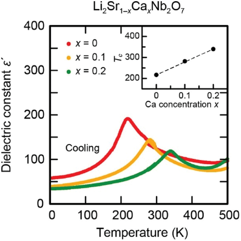
Temperature dependence of the relative permittivity for Li2Sr1–xCaxNb2O7 measured at a frequency of 100 kHz. The inset shows the Ca-content dependence of the ferroelectric phase transition temperature Tc. Adapted with permission from ref. [187]. Copyright 2021 American chemical society.
First-principles calculations provide further insight into the mechanism behind the elevation of Tc due to Ca substitution. Figure 26 presents the COHP and the schematic energy level diagram of Li2CaNb2O7, with the results for Li2SrNb2O7 shown for comparison [187]. The calculations were performed with the Cmcm and Pmcn symmetries, similar to the case of the Ta-substitution effect discussed earlier. Note that the Pmcn structure of Li2CaNb2O7 is obtained by the freezing of the Y2− soft mode (Figure 21(c)) in the Cmcm structure (Figure 21(a)), which was also found to be unstable in the Cmcm structure of Li2CaTa2O7 [188,194]. As shown in Figure 26, the positive – COHP is enhanced by the transformation to the Pmcn structure in Li2CaNb2O7, demonstrating that Ca substitution encourages the instability of the Y2− soft mode. It should be noted that, in contrast to Li2SrNb2O7, a σ-bonding state is markedly enhanced in the Pmcn structure of Li2CaNb2O7. This suggests that the octahedral rotation enhances the overlap between the Nb 4d states and the O 2p states, further motivating the displacement of Nb and leading to the increase of Tc.
Figure 26.
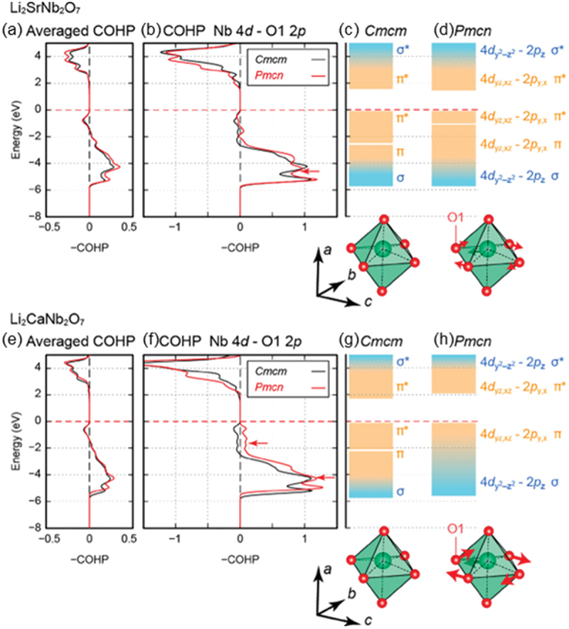
Averaged negative-signed COHPs in (a) Li2SrNb2O7 and (e) Li2CaNb2O7 for all atom pairs with bond lengths less than 3 Å. Negative-signed COHPs between Nb 4d and O 2p states for (b) Li2SrNb2O7 and (f) Li2CaNb2O7 in the cmcm and pmcn phases. Schematic energy level diagrams for the cmcm and pmcn phases of (c, d) Li2SrNb2O7 and (g, h) Li2CaNb2O7 are described. Adapted with permission from ref. [187]. Copyright 2021 American chemical society.
The preceding discussion has clarified that both the SOJT effect and the HIF coexist in the system of Li2SrNb2O7, where Ta-substitution for Nb and Ca-substitution for Sr are capable of tuning the SOJT effect and the HIF, respectively. This paragraph explores the co-substitution effect of Nb and Ca in Li2(Sr1-xCax)(Nb1-xTax)2O7. Figure 27 presents a phase diagram of Li2(Sr1-xCax)(Nb1-xTax)2O7, determined through a combination of dielectric measurements, x-ray diffraction, and second-harmonic generation measurements [188]. While the end-member composition Li2SrNb2O7 undergoes successive phase transitions from I4/mmm to Cmcm and finally to P21cn, the counterpart Li2CaTa2O7 exhibits an antiferroelectric Pmcn structure between the Cmcm and P21cn phases. The ground state throughout the entire composition range is characterized by the P21cn structure, which features in-plane antipolar and out-of-plane polar configurations of the off-center displacement of Nb within the NbO6 octahedron.
Figure 27.
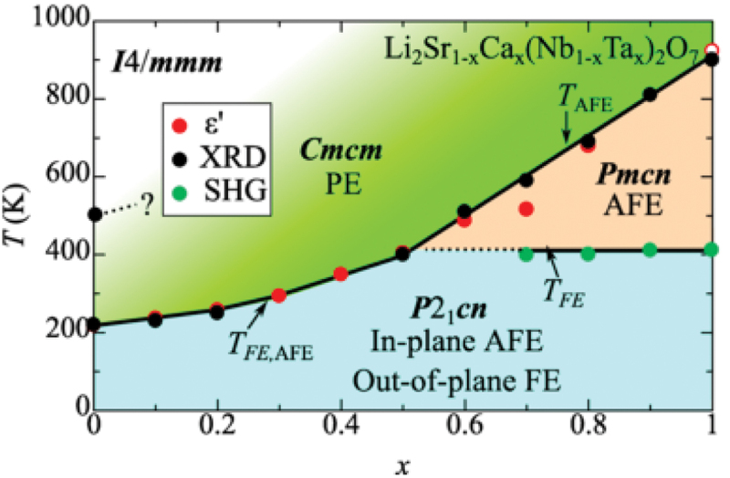
Phase diagram of Li2Sr1–xCax(Nb1–xTax)2O7. The abbreviations PE, AFE, and FE denote paraelectricity, antiferroelectricity, and ferroelectricity, respectively. The open circle data for x = 1 is referred to in ref. [194]. Adapted with permission from ref. [188]. Copyright 2022 American physical society.
One intriguing trend in the phase diagram is that the increase in Tc is significantly weaker compared to the case of single Ca substitution for Sr. This suggests a close competition between the suppression of the SOJT effect due to Ta substitution and the enhancement of the HIF due to Ca substitution. To examine this competition in detail, the magnitude of the SOJT effect () and HIF () has been quantified, where represents the displacement of the B-site cation along the c-axis, and denotes the scale of anisotropy induced by octahedral rotation as shown in Figure 28(a,b) [188]. Figure 28(c) shows the relationship between and across different compositions. It is evident from the figure that the structural instability in Li2SrNb2O7 is primarily governed by the SOJT effect. However, the co-substitution of Ca and Nb enhances the effect of HIF, eventually surpassing the SOJT effect around the composition of x = 0.7. In the end-member composition of Li2CaTa2O7, the HIF becomes dominant in the structural phase transition. The phase diagram’s correspondence with the structural analysis in panel (c) strongly supports the conclusion that the close competition between the SOJT effect and the HIF provides a rich phase instability in the pseudo-RP-type structure.
Figure 28.
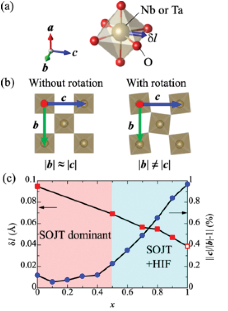
Schematics of (a) the displacement of B-cation in an octahedron, (b) the in-plane lattice anisotropy induced by octahedral rotation. The blue vector in (a) shows the B-cation displacement along the c axis (δl). (c) The x-dependence of δl and lattice anisotropy at 100 K. The open square data for x = 1 is evaluated from room temperature data in tables 1 and 2 in ref. [195] (the two Ta-sites are averaged). Adapted with permission from ref. [188]. Copyright 2022 American physical society.
Combining all the discussions, we can conclude that Li2SrNb2O7 has two coexisting mechanisms: the SOJT effect and the HIF. The SOJT effect is the origin of the Ti displacement for the proper ferroelectrics, such as in BaTiO3 and PbTiO3 [196], whereas the HIF mechanism is triggered by the two octahedral rotational distortions like in Ca3Ti2O7 and Sr3Sn2O7 [179,183]. Li2SrNb2O7 is a unique ferroelectric material that has two ‘switches’ to trigger the phase transition, which is confirmed by partially substituting Ta and/or Ca in Li2SrNb2O7 from the experiments and the calculations. It is noteworthy that these results were reproduced from the synthesis of a single crystal performed by Cheong’s group [197], although our experimental and computational results were partly in contrast to the previous reports [198].
Our study exemplifies how effective collaboration between computational modeling and experimental techniques helps the investigation of ferroelectric materials. Particularly for displacive-type ferroelectrics driven by lattice instability, we have demonstrated that first-principles calculations provide valuable guidelines for the rational design of compositions. These calculations visualize the displacement pattern of the soft mode and reveal corresponding variations in chemical bonding states, offering insights crucial for the systematic development of new materials. This integrated approach not only enhances our understanding of ferroelectric mechanisms but also facilitates targeted material design with enhanced functional properties.
4. Summary and outlook
We have reviewed selected examples of our combined computational and experimental approaches to inorganic semiconductors and dielectrics, covering topics from methodology development to materials design, prediction, and exploration. High-throughput first-principles calculations of polarons, point defects, surfaces, and interfaces enable systematic and accurate predictions of their structures and properties, and the generated data are effectively used for machine learning, as well as the cases of bulk fundamental properties. The constructed machine learning models allow us to predict various material properties and search for promising materials much more quickly than the use of direct theoretical calculations. A great advantage is that a tremendous number of candidate materials can, therefore, be considered, substantially widening the materials search space. However, we need to care about prediction accuracy associated with regression errors, as well as errors inheriting from first-principles calculations. The validation of the machine learning prediction by theoretical calculations and experiments should be important.
To show the effectiveness of the combined computational and experimental approaches in materials research, we have discussed the cases of ternary nitride semiconductors for potential optoelectronic and photovoltaic applications, phosphide-based photovoltaic cells and their constituent phosphide semiconductors, and layered perovskite oxide ferroelectrics. In addition, we have demonstrated the efficient construction of phase diagrams using active learning in conjunction with experiments. This scheme has been applied to the determination of experimental conditions for phosphide film growth.
The combination of theory, computation, and experiment is also useful for unveiling the mechanisms behind material functionalities, which is an important step toward the construction of materials design principles. This is exemplified by the case of the layered perovskite oxide ferroelectrics, where theoretical phonon and chemical bonding analyses help us elucidate the unique origin of their ferroelectricity.
Given the recent worldwide interest in materials informatics, we surely expect that the methodologies and algorithms for theoretical calculations and data scientific methods will be continuously improved and more powerful in materials research. Further development of supercomputers will allow us to generate more accurate and abundant computational materials data, with which machine learning becomes more effective and useable in a wider variety of materials studies. In addition, current trends toward open science will make more computational and experimental materials databases freely available. Effective use of such publicly open data, as well as in-house closed ones, will be a key to conducting cutting-edge data-centric research in the rapidly growing materials informatics field.
Biographies

Fumiyasu Oba is a Professor in the Materials and Structures Laboratory, Institute of Integrated Research at the Institute of Science Tokyo. His primary research interests include computational design and exploration of novel electronic materials, particularly nitride and oxide semiconductors for electronic and photovoltaic applications, from the perspective of band-structure and defect tailoring.

Takayuki Nagai obtained his Ph.D. degree from Nagoya University in 2019. He is currently a Project Assistant Professor in Quantum-Phase Electronics Center, School of Engineering, The University of Tokyo. His research covers solid state physics and inorganic chemistry. His area of interest is design for ferroic/multiferroic materials and new physical phenomena based on symmetry.

Ryoji Katsube received a Ph.D. from Kyoto University in 2018. He worked as a postdoctoral researcher of this project at Kyoto University from 2018 to 2021, focusing on development of phosphide semiconductors for photovoltaics. He is currently a senior lecturer at Department of Materials Process Engineering, Nagoya University, working on the processing of phosphide and group IV semiconductors based on solidification and thermodynamics.

Yasuhide Mochizuki received his Ph.D. degree from Tokyo Institute of Technology in 2021. He is currently an Assistant Professor of Department of Materials Science and Engineering, School of Materials and Chemical Technology, Institute of Science Tokyo. He has broad interests in ferroelectrics, semiconductors, surface structures, negative thermal expansion, and so on, which are centered around the first-principles lattice-dynamics calculations.

Masatake Tsuji obtained his Ph.D. degree from Tokyo Institute of Technology in 2023. He is currently working as a Specially Appointed Assistant Professor of MDX Research Center for Element Strategy, Institute of Integrated Research, Institute of Science Tokyo. His main research area is semiconductor devices such as thin-film transistors, and he is interested in utilization of electronic active defects for the area.

Guillaume Deffrennes is a research fellow at the French National Centre for Scientific Research (CNRS) in the SIMaP laboratory in Grenoble. His primary research focuses on applying machine learning to predict the thermodynamic properties and phase diagrams of alloys. He obtained his Ph.D. in 2018 from Claude Bernard University Lyon 1.

Kota Hanzawa received his Ph.D. degree from Tokyo Institute of Technology in 2019. He is currently an Assistant Professor of Materials and Structures Laboratory, Institute of Integrated Research, Institute of Science Tokyo. He is presently working on exploration of non-oxide semiconductors such as nitrides and chalcogenides, and development of superconductor thin films.

Akitoshi Nakano is currently an Assistant Professor in the Department of Physics, Nagoya University. His research covers solid state physics, inorganic chemistry, materials science, and x-ray diffraction analysis. He currently focuses on the development of low-dimensional functional materials, including ferro/antiferroelectric insulators, magnetic semiconductors, and thermoelectric semimetals.

Akira Takahashi is an assistant professor at the Materials and Structures Laboratory of the Institute of Integrated Research, Institute of Science Tokyo. He has worked in the field of materials science, in particular, his research interests focus on the exploration of dielectrics and semiconductors using materials informatics. He obtained his Ph.D. in 2017 from the Graduate School of Engineering at Kyoto University.

Kei Terayama is an associate professor at the Graduate School of Medical Life Science at Yokohama City University. He received a Doctor of Human and Environmental Studies degree from Kyoto University in 2016. His research interests include the development of machine learning and optimization techniques for materials sciences, drug discovery, and underwater monitoring.

Ryo Tamura is Team Leader at Center for Basic Research on Materials (CBRM) in National Institute for Materials Science (NIMS). He has worked in the field of materials science, in particular, his research interests focus on materials informatics and automated materials explorations. He obtained his Ph.D. in 2012 from Graduate School of Science, University of Tokyo.

Hidenori Hiramatsu is currently a Professor of Materials and Structures Laboratory, Institute of Integrated Research, Institute of Science Tokyo. His research interest focuses on the exploration of optoelectronic properties of novel complex materials by precise control of various experimental techniques such as materials’ synthesis, heteroepitaxial growth, and electronic device fabrication.

Yoshitaro Nose is currently an Associate Professor in the Department of Materials Science and Engineering, Kyoto University. His research topics are the development of novel materials for solar cells, in particular phosphide semiconductors, and processing for devices. He also joins a venture company providing 2D materials, which was established based on his own patents.

Hiroki Taniguchi is currently an Associate Professor in the Department of Physics, Nagoya University. His research covers solid state physics, inorganic chemistry, materials science, and light scattering spectroscopy. He currently focuses on the development of eco-friendly functional oxides, including high-k dielectric, ferro/antiferroelectric, piezoelectric, and optically tunable dielectric materials.
Funding Statement
The work was supported mainly by the CREST project from Japan Science and Technology Corporation [JPMJCR17J2].
Disclosure statement
No potential conflict of interest was reported by the author(s).
References
- [1].Hosono H. Exploring electro-active functionality of transparent oxide materials. Jpn J Appl Phys. 2013;52(9R):090001. doi: 10.7567/JJAP.52.090001 [DOI] [Google Scholar]
- [2].Kim JY, Lee J-W, Jung HS, et al. High-efficiency perovskite solar cells. Chem Rev. 2020;120(15):7867–33. doi: 10.1021/acs.chemrev.0c00107 [DOI] [PubMed] [Google Scholar]
- [3].Yang SY, Seidel J, Byrnes SJ, et al. Above-bandgap voltages from ferroelectric photovoltaic devices. Nat Nanotechnol. 2010;5(2):143–147. doi: 10.1038/nnano.2009.451 [DOI] [PubMed] [Google Scholar]
- [4].Fichtner S, Wolff N, Lofink F, et al. AlScN: a III-V semiconductor based ferroelectric. J Appl Phys. 2019;125(11). doi: 10.1063/1.5084945 [DOI] [Google Scholar]
- [5].Park MH, Lee YH, Mikolajick T, et al. Review and perspective on ferroelectric HfO2-based thin films for memory applications. MRS Commun. 2018;8(3):795–808. doi: 10.1557/mrc.2018.175 [DOI] [Google Scholar]
- [6].Mikolajick T, Slesazeck S, Park MH, et al. Ferroelectric hafnium oxide for ferroelectric random-access memories and ferroelectric field-effect transistors. MRS Bull. 2018;43(5):340–346. doi: 10.1557/mrs.2018.92 [DOI] [Google Scholar]
- [7].Coll M, Fontcuberta J, Althammer M, et al. Towards oxide electronics: a roadmap. Appl Surf Sci. 2019;482:1–93. doi: 10.1016/j.apsusc.2019.03.312 [DOI] [Google Scholar]
- [8].Vaz CAF, Shin YJ, Bibes M, et al. Epitaxial ferroelectric interfacial devices. Appl Phys Rev. 2021;8(4). doi: 10.1063/5.0060218 [DOI] [Google Scholar]
- [9].Martin RM. Electronic structure: basic theory and practical methods. 2nd ed. Cambridge (UK): Cambridge University Press; 2020. [Google Scholar]
- [10].Kohanoff J. Electronic structure calculations for solids and molecules: theory and computational methods. Cambridge (UK): Cambridge University Press; 2010. [Google Scholar]
- [11].Giustino F. Materials modelling using density functional theory: properties and predictions. Oxford (UK): Oxford University Press; 2014. [Google Scholar]
- [12].Curtarolo S, Hart GLW, Nardelli MB, et al. The high-throughput highway to computational materials design. Nat Mater. 2013;12(3):191–201. doi: 10.1038/nmat3568 [DOI] [PubMed] [Google Scholar]
- [13].Oba F, Kumagai Y. Design and exploration of semiconductors from first principles: a review of recent advances. Appl Phys Express. 2018;11(6):060101. doi: 10.7567/APEX.11.060101 [DOI] [Google Scholar]
- [14].Butler KT, Davies DW, Cartwright H, et al. Machine learning for molecular and materials science. Nature. 2018;559(7715):547–555. doi: 10.1038/s41586-018-0337-2 [DOI] [PubMed] [Google Scholar]
- [15].Pollice R, dos Passos Gomes G, Aldeghi M, et al. Data-driven strategies for accelerated materials design. Acc Chem Res. 2021;54(4):849–860. doi: 10.1021/acs.accounts.0c00785 [DOI] [PMC free article] [PubMed] [Google Scholar]
- [16].Terayama K, Sumita M, Tamura R, et al. Black-box optimization for automated discovery. Acc Chem Res. 2021;54(6):1334–1346. doi: 10.1021/acs.accounts.0c00713 [DOI] [PubMed] [Google Scholar]
- [17].Jain A, Ong SP, Hautier G, et al. Commentary: the materials project: a materials genome approach to accelerating materials innovation. APL Mater. 2013;1(1):011002. doi: 10.1063/1.4812323 [DOI] [Google Scholar]
- [18].Curtarolo S, Setyawan W, Wang S, et al. AFLOWLIB.ORG: a distributed materials properties repository from high-throughput ab initio calculations. Comput Mater Sci. 2012;58:227–235. doi: 10.1016/j.commatsci.2012.02.002 [DOI] [Google Scholar]
- [19].Kirklin S, Saal JE, Meredig B, et al. The open quantum materials database (OQMD): assessing the accuracy of DFT formation energies. npj Comput Mater. 2015;1(1):15010. doi: 10.1038/npjcompumats.2015.10 [DOI] [Google Scholar]
- [20].Ortiz C, Eriksson O, Klintenberg M. Data mining and accelerated electronic structure theory as a tool in the search for new functional materials. Comput Mater Sci. 2009;44(4):1042–1049. doi: 10.1016/j.commatsci.2008.07.016 [DOI] [Google Scholar]
- [21].Jain A, Hautier G, Moore CJ, et al. A high-throughput infrastructure for density functional theory calculations. Comput Mater Sci. 2011;50(8):2295–2310. doi: 10.1016/j.commatsci.2011.02.023 [DOI] [Google Scholar]
- [22].Talirz L, Kumbhar S, Passaro E, et al. Materials cloud, a platform for open computational science. Sci Data. 2020;7(1):299. doi: 10.1038/s41597-020-00637-5 [DOI] [PMC free article] [PubMed] [Google Scholar]
- [23].Ghiringhelli LM, Carbogno C, Levchenko S, et al. Towards efficient data exchange and sharing for big-data driven materials science: metadata and data formats. npj Comput Mater. 2017;3(1):46. doi: 10.1038/s41524-017-0048-5 [DOI] [Google Scholar]
- [24].Xu Y, Yamazaki M, Villars P. Inorganic materials database for exploring the nature of material. Jpn J Appl Phys. 2011;50(11S):11RH02. doi: 10.1143/JJAP.50.11RH02 [DOI] [Google Scholar]
- [25].Zakutayev A, Wunder N, Schwarting M, et al. An open experimental database for exploring inorganic materials. Sci Data. 2018;5(1):180053. doi: 10.1038/sdata.2018.53 [DOI] [PMC free article] [PubMed] [Google Scholar]
- [26].Gake T, Kumagai Y, Oba F. First-principles study of self-trapped holes and acceptor impurities in Ga2O3 polymorphs. Phys Rev Mater. 2019;3(4):044603. doi: 10.1103/PhysRevMaterials.3.044603 [DOI] [Google Scholar]
- [27].Nagafuji T, Osuna K, Hanzawa K, et al. Carrier generation and compensation mechanism in La2SnO2S3. J Mater Chem C. 2024;12(31):12015–12025. doi: 10.1039/D4TC01116C [DOI] [Google Scholar]
- [28].Tsunoda N, Kumagai Y, Oba F. Stabilization of small polarons in BaTiO3 by local distortions. Phys Rev Mater. 2019;3(11):114602. doi: 10.1103/PhysRevMaterials.3.114602 [DOI] [Google Scholar]
- [29].Oba F, Togo A, Tanaka I, et al. Defect energetics in ZnO: a hybrid hartree-fock density functional study. Phys Rev B. 2008;77(24):245202. doi: 10.1103/PhysRevB.77.245202 [DOI] [Google Scholar]
- [30].Kumagai Y, Oba F. Electrostatics-based finite-size corrections for first-principles point defect calculations. Phys Rev B. 2014;89(19):195205. doi: 10.1103/PhysRevB.89.195205 [DOI] [Google Scholar]
- [31].Matsuzaki K, Harada K, Kumagai Y, et al. High-mobility p-type and n-type copper nitride semiconductors by direct nitriding synthesis and in silico doping design. Adv Mater. 2018;30(31):1801968. doi: 10.1002/adma.201801968 [DOI] [PubMed] [Google Scholar]
- [32].Tsunoda N, Kumagai Y, Araki M, et al. One-dimensionally extended oxygen vacancy states in perovskite oxides. Phys Rev B. 2019;99(6):060103. doi: 10.1103/PhysRevB.99.060103 [DOI] [Google Scholar]
- [33].Gake T, Kumagai Y, Freysoldt C, et al. Finite-size corrections for defect-involving vertical transitions in supercell calculations. Phys Rev B. 2020;101(2):020102. doi: 10.1103/PhysRevB.101.020102 [DOI] [Google Scholar]
- [34].Kumagai Y, Tsunoda N, Takahashi A, et al. Insights into oxygen vacancies from high-throughput first-principles calculations. Phys Rev Mater. 2021;5(12):123803. doi: 10.1103/PhysRevMaterials.5.123803 [DOI] [Google Scholar]
- [35].Tsunoda N, Kumagai Y, Oba F. Recommendation of interstitial hydrogen positions in metal oxides. Comput Mater Sci. 2022;203:111068. doi: 10.1016/j.commatsci.2021.111068 [DOI] [Google Scholar]
- [36].Ishii T, Takahashi A, Nagafuji T, et al. Oxygen vacancies in α-(AlxGa1−x)2O3 alloys: a first-principles study. Appl Phys Express. 2023;16(6):061002. doi: 10.35848/1882-0786/acd983 [DOI] [Google Scholar]
- [37].Gake T, Kumagai Y, Takahashi A, et al. Defect formation and carrier compensation in layered oxychalcogenide La2CdO2Se2: an insight from first principles. J Mater Chem C. 2022;10(44):16828–16837. doi: 10.1039/D2TC03836F [DOI] [Google Scholar]
- [38].Kumagai Y, Harada K, Akamatsu H, et al. Carrier-induced band-gap variation and point defects in Zn3N2 from first principles. Phys Rev Appl. 2017;8(1):014015. doi: 10.1103/PhysRevApplied.8.014015 [DOI] [Google Scholar]
- [39].Oba F, Choi M, Togo A, et al. Point defects in ZnO: an approach from first principles. Sci Technol Adv Mater. 2011;12(3):034302. doi: 10.1088/1468-6996/12/3/034302 [DOI] [PMC free article] [PubMed] [Google Scholar]
- [40].Hinuma Y, Oba F, Tanaka I. Valence band offsets at zinc-blende heterointerfaces with misfit dislocations: a first-principles study. Phys Rev B. 2013;88(7):075319. doi: 10.1103/PhysRevB.88.075319 [DOI] [Google Scholar]
- [41].Hinuma Y, Grüneis A, Kresse G, et al. Band alignment of semiconductors from density-functional theory and many-body perturbation theory. Phys Rev B. 2014;90(15):155405. doi: 10.1103/PhysRevB.90.155405 [DOI] [Google Scholar]
- [42].Hinuma Y, Kumagai Y, Oba F, et al. Categorization of surface polarity from a crystallographic approach. Comput Mater Sci. 2016;113:221–230. doi: 10.1016/j.commatsci.2015.11.042 [DOI] [Google Scholar]
- [43].Sung H-J, Mochizuki Y, Oba F. Surface reconstruction and band alignment of nonmetallic A(II)B(IV)O3 perovskites. Phys Rev Mater. 2020;4(4):044606. doi: 10.1103/PhysRevMaterials.4.044606 [DOI] [Google Scholar]
- [44].Hinuma Y, Kumagai Y, Tanaka I, et al. Band alignment of semiconductors and insulators using dielectric-dependent hybrid functionals: toward high-throughput evaluation. Phys Rev B. 2017;95(7):075302. doi: 10.1103/PhysRevB.95.075302 [DOI] [Google Scholar]
- [45].Hinuma Y, Kumagai Y, Tanaka I, et al. Effects of composition, crystal structure, and surface orientation on band alignment of divalent metal oxides: a first-principles study. Phys Rev Mater. 2018;2(12):124603. doi: 10.1103/PhysRevMaterials.2.124603 [DOI] [Google Scholar]
- [46].Wang T, Oba F. Slab surface passivation and its application to band offset calculations for polar heterointerfaces of zinc-blende semiconductors. Phys Rev Mater. 2023;7(8):084602. doi: 10.1103/PhysRevMaterials.7.084602 [DOI] [Google Scholar]
- [47].Mochizuki Y, Sung H-J, Gake T, et al. Chemical trends of surface reconstruction and band positions of nonmetallic perovskite oxides from first principles. Chem Mater. 2023;35(5):2047–2057. doi: 10.1021/acs.chemmater.2c03615 [DOI] [Google Scholar]
- [48].Hinuma Y, Oba F, Kumagai Y, et al. Ionization potentials of (112) and (11) facet surfaces of CuInSe2 and CuGaSe2. Phys Rev B. 2012;86(24):245433. doi: 10.1103/PhysRevB.86.245433 [DOI] [Google Scholar]
- [49].Kiyohara S, Hinuma Y, Oba F. Band alignment of oxides by learnable structural-descriptor-aided neural network and transfer learning. J Am Chem Soc. 2024;146(14):9697–9708. doi: 10.1021/jacs.3c13574 [DOI] [PMC free article] [PubMed] [Google Scholar]
- [50].Oba F, Ohta H, Sato Y, et al. Atomic structure of [0001]-tilt grain boundaries in ZnO: a high-resolution TEM study of fiber-textured thin films. Phys Rev B. 2004;70(12):125415. doi: 10.1103/PhysRevB.70.125415 [DOI] [Google Scholar]
- [51].Hinuma Y, Oba F, Kumagai Y, et al. Band offsets of CuInSe2/CdS and CuInSe2/ZnS (110) interfaces: a hybrid density functional theory study. Phys Rev B. 2013;88(3):035305. doi: 10.1103/PhysRevB.88.035305 [DOI] [Google Scholar]
- [52].Grüneis A, Kresse G, Hinuma Y, et al. Ionization potentials of solids: the importance of vertex corrections. Phys Rev Lett. 2014;112(9):096401. doi: 10.1103/PhysRevLett.112.096401 [DOI] [PubMed] [Google Scholar]
- [53].Kuroiwa Y, Matsushita Y-I, Harada K, et al. Theoretical prediction of strain-induced carrier effective mass modulation in 4H-SiC and GaN. Appl Phys Lett. 2019;115(11). doi: 10.1063/1.5122215 [DOI] [Google Scholar]
- [54].Kuroiwa Y, Matsushita Y-I, Oba F. Unraveling crystal symmetry and strain effects on electronic band structures of SiC polytypes. AIP Adv. 2020;10(10). doi: 10.1063/5.0010512 [DOI] [Google Scholar]
- [55].Takahashi A, Kumagai Y, Miyamoto J, et al. Machine learning models for predicting the dielectric constants of oxides based on high-throughput first-principles calculations. Phys Rev Mater. 2020;4(10):103801. doi: 10.1103/PhysRevMaterials.4.103801 [DOI] [Google Scholar]
- [56].Hinuma Y, Hayashi H, Kumagai Y, et al. Comparison of approximations in density functional theory calculations: energetics and structure of binary oxides. Phys Rev B. 2017;96(9):094102. doi: 10.1103/PhysRevB.96.094102 [DOI] [Google Scholar]
- [57].Yokoyama T, Oba F, Seko A, et al. Theoretical photovoltaic conversion efficiencies of ZnSnP2, CdSnP2, and Zn1-xCdxSnP2 alloys. Appl Phys Express. 2013;6(6):061201. doi: 10.7567/APEX.6.061201 [DOI] [Google Scholar]
- [58].Mochizuki Y, Sung H-J, Takahashi A, et al. Theoretical exploration of mixed-anion antiperovskite semiconductors M3XN (M=Mg, Ca, Sr, Ba; X=P, As, Sb, Bi). Phys Rev Mater. 2020;4(4):044601. doi: 10.1103/PhysRevMaterials.4.044601 [DOI] [Google Scholar]
- [59].Blöchl PE. Projector augmented-wave method. Phys Rev B. 1994;50(24):17953–17979. doi: 10.1103/PhysRevB.50.17953 [DOI] [PubMed] [Google Scholar]
- [60].Kresse G, Furthmüller J. Efficient iterative schemes for ab initio total-energy calculations using a plane-wave basis set. Phys Rev B. 1996;54(16):11169–11186. doi: 10.1103/PhysRevB.54.11169 [DOI] [PubMed] [Google Scholar]
- [61].Kresse G, Joubert D. From ultrasoft pseudopotentials to the projector augmented-wave method. Phys Rev B. 1999;59(3):1758–1775. doi: 10.1103/PhysRevB.59.1758 [DOI] [Google Scholar]
- [62].Gake T, Kumagai Y, Takahashi A, et al. Point defects in p-type transparent conductive CuMO2 (M = Al, Ga, In) from first principles. Phys Rev Mater. 2021;5(10):104602. doi: 10.1103/PhysRevMaterials.5.104602 [DOI] [Google Scholar]
- [63].Freysoldt C, Neugebauer J, Van de Walle CG. Fully ab initio finite-size corrections for charged-defect supercell calculations. Phys Rev Lett. 2009;102(1):016402. doi: 10.1103/PhysRevLett.102.016402 [DOI] [PubMed] [Google Scholar]
- [64].Kohn W, Sham LJ. Self-consistent equations including exchange and correlation effects. Phys Rev. 1965;140(4A):A1133–A1138. doi: 10.1103/PhysRev.140.A1133 [DOI] [Google Scholar]
- [65].Vosko SH, Wilk L, Nusair M. Accurate spin-dependent electron liquid correlation energies for local spin density calculations: a critical analysis. Can J Phys. 1980;58(8):1200–1211. doi: 10.1139/p80-159 [DOI] [Google Scholar]
- [66].Perdew JP, Zunger A. Self-interaction correction to density-functional approximations for many-electron systems. Phys Rev B. 1981;23(10):5048–5079. doi: 10.1103/PhysRevB.23.5048 [DOI] [Google Scholar]
- [67].Becke AD. Density-functional exchange-energy approximation with correct asymptotic behavior. Phys Rev A. 1988;38(6):3098–3100. doi: 10.1103/PhysRevA.38.3098 [DOI] [PubMed] [Google Scholar]
- [68].Perdew JP, Wang Y. Accurate and simple analytic representation of the electron-gas correlation energy. Phys Rev B. 1992;45(23):13244–13249. doi: 10.1103/PhysRevB.45.13244 [DOI] [PubMed] [Google Scholar]
- [69].Perdew JP, Burke K, Ernzerhof M. Generalized gradient approximation made simple. Phys Rev Lett. 1996;77(18):3865–3868. doi: 10.1103/PhysRevLett.77.3865 [DOI] [PubMed] [Google Scholar]
- [70].Perdew JP, Ruzsinszky A, Csonka GI, et al. Restoring the density-gradient expansion for exchange in solids and surfaces. Phys Rev Lett. 2008;100(13):136406. doi: 10.1103/PhysRevLett.100.136406 [DOI] [PubMed] [Google Scholar]
- [71].Hohenberg P, Kohn W. Inhomogeneous electron gas. Phys Rev. 1964;136(3B):B864–B871. doi: 10.1103/PhysRev.136.B864 [DOI] [Google Scholar]
- [72].Anisimov VI, Zaanen J, Andersen OK. Band theory and Mott insulators: Hubbard U instead of Stoner I. Phys Rev B. 1991;44(3):943–954. doi: 10.1103/PhysRevB.44.943 [DOI] [PubMed] [Google Scholar]
- [73].Dudarev SL, Botton GA, Savrasov SY, et al. Electron-energy-loss spectra and the structural stability of nickel oxide: an LSDA+U study. Phys Rev B. 1998;57(3):1505–1509. doi: 10.1103/PhysRevB.57.1505 [DOI] [Google Scholar]
- [74].Perdew JP, Ernzerhof M, Burke K. Rationale for mixing exact exchange with density functional approximations. J Chem Phys. 1996;105(22):9982–9985. doi: 10.1063/1.472933 [DOI] [Google Scholar]
- [75].Adamo C, Barone V. Toward reliable density functional methods without adjustable parameters: the PBE0 model. J Chem Phys. 1999;110(13):6158–6170. doi: 10.1063/1.478522 [DOI] [Google Scholar]
- [76].Heyd J, Scuseria GE, Ernzerhof M. Hybrid functionals based on a screened Coulomb potential. J Chem Phys. 2003;118(18):8207–8215. doi: 10.1063/1.1564060 [DOI] [Google Scholar]
- [77].Becke AD. Density‐functional thermochemistry. III. The role of exact exchange. J Chem Phys. 1993;98(7):5648–5652. doi: 10.1063/1.464913 [DOI] [Google Scholar]
- [78].Marques MAL, Vidal J, Oliveira MJT, et al. Density-based mixing parameter for hybrid functionals. Phys Rev B. 2011;83(3):035119. doi: 10.1103/PhysRevB.83.035119 [DOI] [Google Scholar]
- [79].Alkauskas A, Broqvist P, Pasquarello A. Defect levels through hybrid density functionals: insights and applications. Phys Status Solidi B. 2011;248(4):775–789. doi: 10.1002/pssb.201046195 [DOI] [Google Scholar]
- [80].Skone JH, Govoni M, Galli G. Self-consistent hybrid functional for condensed systems. Phys Rev B. 2014;89(19):195112. doi: 10.1103/PhysRevB.89.195112 [DOI] [Google Scholar]
- [81].Gerosa M, Bottani CE, Di Valentin C, et al. Accuracy of dielectric-dependent hybrid functionals in the prediction of optoelectronic properties of metal oxide semiconductors: a comprehensive comparison with many-body GW and experiments. J Phys Condens Matter. 2018;30(4):044003. doi: 10.1088/1361-648X/aa9725 [DOI] [PubMed] [Google Scholar]
- [82].Hinuma Y, Gake T, Oba F. Band alignment at surfaces and heterointerfaces of Al2O3, Ga2O3, In2O3, and related group-III oxide polymorphs: a first-principles study. Phys Rev Mater. 2019;3(8):084605. doi: 10.1103/PhysRevMaterials.3.084605 [DOI] [Google Scholar]
- [83].Hedin L. New method for calculating the one-particle green’s function with application to the electron-gas problem. Phys Rev. 1965;139(3A):A796–A823. doi: 10.1103/PhysRev.139.A796 [DOI] [Google Scholar]
- [84].Vidal J, Trani F, Bruneval F, et al. Effects of electronic and lattice polarization on the band structure of delafossite transparent conductive oxides. Phys Rev Lett. 2010;104(13):136401. doi: 10.1103/PhysRevLett.104.136401 [DOI] [PubMed] [Google Scholar]
- [85].Kiyohara S, Mora-Fonz D, Shluger A, et al. Unique atomic and electronic structures of oxygen vacancies in amorphous SnO2 from first principles and informatics. J Phys Chem C. 2022;126(44):18833–18838. doi: 10.1021/acs.jpcc.2c04764 [DOI] [Google Scholar]
- [86].Choi M, Oba F, Tanaka I. Role of Ti antisitelike defects in SrTiO3. Phys Rev Lett. 2009;103(18):185502. doi: 10.1103/PhysRevLett.103.185502 [DOI] [PubMed] [Google Scholar]
- [87].Choi M, Oba F, Kumagai Y, et al. Anti-ferrodistortive-like oxygen-octahedron rotation induced by the oxygen vacancy in cubic SrTiO3. Adv Mater. 2013;25(1):86–90. doi: 10.1002/adma.201203580 [DOI] [PubMed] [Google Scholar]
- [88].Ishikawa R, Shibata N, Oba F, et al. Functional complex point-defect structure in a huge-size-mismatch system. Phys Rev Lett. 2013;110(6):065504. doi: 10.1103/PhysRevLett.110.065504 [DOI] [PubMed] [Google Scholar]
- [89].Cahen D, Kahn A. Electron energetics at surfaces and interfaces: concepts and experiments. Adv Mater. 2003;15(4):271–277. doi: 10.1002/adma.200390065 [DOI] [Google Scholar]
- [90].Ping Y, Rocca D, Galli G. Electronic excitations in light absorbers for photoelectrochemical energy conversion: first principles calculations based on many body perturbation theory. Chem Soc Rev. 2013;42(6):2437–2469. doi: 10.1039/C3CS00007A [DOI] [PubMed] [Google Scholar]
- [91].Kim S, Sinai O, Lee C-W, et al. Controlling oxide surface dipole and reactivity with intrinsic nonstoichiometric epitaxial reconstructions. Phys Rev B. 2015;92(23):235431. doi: 10.1103/PhysRevB.92.235431 [DOI] [Google Scholar]
- [92].Kumagai Y, Burton LA, Walsh A, et al. Electronic structure and defect physics of tin sulfides: SnS, Sn2S3, and SnS2. Phys Rev Appl. 2016;6(1):014009. doi: 10.1103/PhysRevApplied.6.014009 [DOI] [Google Scholar]
- [93].Kumagai Y, Butler KT, Walsh A, et al. Theory of ionization potentials of nonmetallic solids. Phys Rev B. 2017;95(12):125309. doi: 10.1103/PhysRevB.95.125309 [DOI] [Google Scholar]
- [94].Henrich VE, Cox PA. The surface science of metal oxides. Cambridge (UK): Cambridge University Press; 1996. [Google Scholar]
- [95].Mönch W. Semiconductor surfaces and interfaces. Heidelberg: Springer; 2001. [Google Scholar]
- [96].Castell MR. Scanning tunneling microscopy of reconstructions on the SrTiO3(001) surface. Surf Sci. 2002;505:1–13. doi: 10.1016/S0039-6028(02)01393-6 [DOI] [Google Scholar]
- [97].Dulub O, Diebold U, Kresse G. Novel stabilization mechanism on polar surfaces: ZnO(0001)-Zn. Phys Rev Lett. 2003;90(1):016102. doi: 10.1103/PhysRevLett.90.016102 [DOI] [PubMed] [Google Scholar]
- [98].Setvin M, Reticcioli M, Poelzleitner F, et al. Polarity compensation mechanisms on the perovskite surface KTaO3(001). Science. 2018;359(6375):572–575. doi: 10.1126/science.aar2287 [DOI] [PubMed] [Google Scholar]
- [99].Deacon-Smith DEE, Scanlon DO, Catlow CRA, et al. Interlayer cation exchange stabilizes polar perovskite surfaces. Adv Mater. 2014;26(42):7252–7256. doi: 10.1002/adma.201401858 [DOI] [PMC free article] [PubMed] [Google Scholar]
- [100].Bartók AP, Kondor R, Csányi G. On representing chemical environments. Phys Rev B. 2013;87(18):184115. doi: 10.1103/PhysRevB.87.184115 [DOI] [Google Scholar]
- [101].Motoyama Y, Tamura R, Yoshimi K, et al. Bayesian optimization package: PHYSBO. Comput Phys Commun. 2022;278:108405. doi: 10.1016/j.cpc.2022.108405 [DOI] [Google Scholar]
- [102].Kishio T, Kaneko H, Funatsu K. Strategic parameter search method based on prediction errors and data density for efficient product design. Chemom Intell Lab Syst. 2013;127:70–79. doi: 10.1016/j.chemolab.2013.06.002 [DOI] [Google Scholar]
- [103].Takahashi A, Kumagai Y, Aoki H, et al. Adaptive sampling methods via machine learning for materials screening. Sci Technol Adv Mater Meth. 2022;2(1):55–66. doi: 10.1080/27660400.2022.2039573 [DOI] [Google Scholar]
- [104].Terayama K, Sumita M, Tamura R, et al. Pushing property limits in materials discovery via boundless objective-free exploration. Chem Sci. 2020;11(23):5959–5968. doi: 10.1039/D0SC00982B [DOI] [PMC free article] [PubMed] [Google Scholar]
- [105].Takahashi A, Terayama K, Kumagai Y, et al. Fully autonomous materials screening methodology combining first-principles calculations, machine learning and high-performance computing system. Sci Technol Adv Mater Meth. 2023;3(1):2261834. doi: 10.1080/27660400.2023.2261834 [DOI] [Google Scholar]
- [106].Sato N, Takahashi A, Kiyohara S, et al. Target material property-dependent cluster analysis of inorganic compounds. Adv Intell Syst. 2024:2400253. doi: 10.1002/aisy.202400253 [DOI] [Google Scholar]
- [107].Terayama K, Tamura R, Nose Y, et al. Efficient construction method for phase diagrams using uncertainty sampling. Phys Rev Mater. 2019;3(3):033802. doi: 10.1103/PhysRevMaterials.3.033802 [DOI] [Google Scholar]
- [108].Spencer PJ. A brief history of CALPHAD. Calphad. 2008;32(1):1–8. doi: 10.1016/j.calphad.2007.10.001 [DOI] [Google Scholar]
- [109].Katsube R, Terayama K, Tamura R, et al. Experimental establishment of phase diagrams guided by uncertainty sampling: an application to the deposition of Zn–Sn–P films by molecular beam epitaxy. ACS Mater Lett. 2020;2(6):571–575. doi: 10.1021/acsmaterialslett.0c00104 [DOI] [Google Scholar]
- [110].Terayama K, Han K, Katsube R, et al. Acceleration of phase diagram construction by machine learning incorporating Gibbs’ phase rule. Scr Mater. 2022;208:114335. doi: 10.1016/j.scriptamat.2021.114335 [DOI] [Google Scholar]
- [111].Tamura R, Deffrennes G, Han K, et al. Machine-learning-based phase diagram construction for high-throughput batch experiments. Sci Technol Adv Mater Meth. 2022;2(1):153–161. doi: 10.1080/27660400.2022.2076548 [DOI] [Google Scholar]
- [112].Tamura R, Morito H, Deffrennes G, et al. AIPHAD, an active learning web application for visual understanding of phase diagrams. Commun Mater. 2024;5(1). doi: 10.1038/s43246-024-00580-7 [DOI] [Google Scholar]
- [113].Deffrennes G, Terayama K, Abe T, et al. A machine learning–based classification approach for phase diagram prediction. Mater Des. 2022;215:110497. doi: 10.1016/j.matdes.2022.110497 [DOI] [Google Scholar]
- [114].Deffrennes G, Terayama K, Abe T, et al. A framework to predict binary liquidus by combining machine learning and CALPHAD assessments. Mater Des. 2023;232:112111. doi: 10.1016/j.matdes.2023.112111 [DOI] [Google Scholar]
- [115].Miedema AR, De Boer FR, Boom R. Predicting heat effects in alloys. Physica B+C. 1981;103(1):67–81. doi: 10.1016/0378-4363(81)91003-2 [DOI] [Google Scholar]
- [116].Gautier R, Zhang X, Hu L, et al. Prediction and accelerated laboratory discovery of previously unknown 18-electron ABX compounds. Nat Chem. 2015;7(4):308–316. doi: 10.1038/nchem.2207 [DOI] [PubMed] [Google Scholar]
- [117].Hinuma Y, Hatakeyama T, Kumagai Y, et al. Discovery of earth-abundant nitride semiconductors by computational screening and high-pressure synthesis. Nat Commun. 2016;7(1):11962. doi: 10.1038/ncomms11962 [DOI] [PMC free article] [PubMed] [Google Scholar]
- [118].Zakutayev A, Bauers SR, Lany S. Experimental synthesis of theoretically predicted multivalent ternary nitride materials. Chem Mater. 2022;34(4):1418–1438. doi: 10.1021/acs.chemmater.1c03014 [DOI] [Google Scholar]
- [119].Sarker P, Harrington T, Toher C, et al. High-entropy high-hardness metal carbides discovered by entropy descriptors. Nat Commun. 2018;9(1):4980. doi: 10.1038/s41467-018-07160-7 [DOI] [PMC free article] [PubMed] [Google Scholar]
- [120].Sun W, Bartel CJ, Arca E, et al. A map of the inorganic ternary metal nitrides. Nat Mater. 2019;18(7):732–739. doi: 10.1038/s41563-019-0396-2 [DOI] [PubMed] [Google Scholar]
- [121].Oba F. Computational design and exploration of nitride and oxide semiconductors. J Ceram Soc Jpn. 2023;131(8):392–397. doi: 10.2109/jcersj2.23085 [DOI] [Google Scholar]
- [122].Kikuchi R, Ueno K, Nakamura T, et al. SrZn2N2 as a solar absorber: theoretical defect chemistry and synthesis by metal alloy nitridation. Chem Mater. 2021;33(8):2864–2870. doi: 10.1021/acs.chemmater.1c00075 [DOI] [Google Scholar]
- [123].Kikuchi R, Nakamura T, Kurabuchi T, et al. Theoretical prediction and thin-film growth of the defect-tolerant nitride semiconductor YZn3N3. Chem Mater. 2021;33(21):8205–8211. doi: 10.1021/acs.chemmater.1c02149 [DOI] [Google Scholar]
- [124].Hayashi H, Katayama S, Komura T, et al. Discovery of a novel Sn(II)-based oxide β-SnMoO4 for Daylight-Driven Photocatalysis. Adv Sci. 2017;4(1):1600246. doi: 10.1002/advs.201600246 [DOI] [PMC free article] [PubMed] [Google Scholar]
- [125].Tsuji M, Hiramatsu H, Hosono H. Tunable light emission through the range 1.8–3.2 eV and p-type conductivity at room temperature for nitride semiconductors, Ca(Mg1–xZnx)2N2 (x = 0–1). Inorg Chem. 2019;58(18):12311–12316. doi: 10.1021/acs.inorgchem.9b01811 [DOI] [PubMed] [Google Scholar]
- [126].Tsuji M, Hanzawa K, Kinjo H, et al. Heteroepitaxial thin-film growth of a ternary nitride semiconductor CaZn2N2. ACS Appl Electron Mater. 2019;1(8):1433–1438. doi: 10.1021/acsaelm.9b00248 [DOI] [Google Scholar]
- [127].Orisakwe E, Fontaine B, Gregory DH, et al. Theoretical study on the structural, electronic and physical properties of layered alkaline-earth-group-4 transition-metal nitrides AEMN2. RSC Adv. 2014;4(60):31981–31987. doi: 10.1039/C4RA05395H [DOI] [Google Scholar]
- [128].Greenaway AL, Melamed CL, Tellekamp MB, et al. Ternary nitride materials: fundamentals and emerging device applications. Annu Rev Mater Res. 2021;51(1):591–618. doi: 10.1146/annurev-matsci-080819-012444 [DOI] [Google Scholar]
- [129].Brese NE, DiSalvo FJ. Synthesis of the first thorium-containing nitride perovskite, TaThN3. J Solid State Chem. 1995;120(2):378–380. doi: 10.1006/jssc.1995.1423 [DOI] [Google Scholar]
- [130].Niewa R. Metal-Rich Ternary Perovskite Nitrides. Eur J Inorg Chem. 2019;2019(32):3647–3660. doi: 10.1002/ejic.201900756 [DOI] [Google Scholar]
- [131].Sarmiento-Pérez R, Cerqueira TFT, Körbel S, et al. Prediction of stable nitride perovskites. Chem Mater. 2015;27(17):5957–5963. doi: 10.1021/acs.chemmater.5b02026 [DOI] [Google Scholar]
- [132].Kloß SD, Weidemann ML, Attfield JP. Preparation of bulk-phase nitride perovskite LaReN3 and topotactic reduction to LaNiO2-Type LaReN2. Angew Chem Int Ed. 2021;60(41):22260–22264. doi: 10.1002/anie.202108759 [DOI] [PubMed] [Google Scholar]
- [133].Talley KR, Perkins CL, Diercks DR, et al. Synthesis of LaWN3 nitride perovskite with polar symmetry. Science. 2021;374(6574):1488–1491. doi: 10.1126/science.abm3466 [DOI] [PubMed] [Google Scholar]
- [134].Matsuishi S, Iwasaki D, Hosono H. Synthesis of perovskite-type LaWN3 by high-pressure solid-state metathesis reaction. J Solid State Chem. 2022;315:123508. doi: 10.1016/j.jssc.2022.123508 [DOI] [Google Scholar]
- [135].Hanzawa K, Hiramatsu H. Heteroepitaxial growth, degenerate state, and superconductivity of perovskite-type LaWN3 thin films. ACS Appl Electron Mater. 2023;5(5):2793–2798. doi: 10.1021/acsaelm.3c00249 [DOI] [Google Scholar]
- [136].Zhou X, Xu W, Gui Z, et al. Polar nitride perovskite LaWN3-δ with orthorhombic structure. Adv Sci. 2023;10(19):2205479. doi: 10.1002/advs.202205479 [DOI] [PMC free article] [PubMed] [Google Scholar]
- [137].Shiraishi A, Kimura S, He X, et al. Design, synthesis, and optoelectronic properties of the high-purity phase in layered AETMN2 (AE = Sr, Ba; TM = Ti, Zr, Hf) semiconductors. Inorg Chem. 2022;61(17):6650–6659. doi: 10.1021/acs.inorgchem.2c00604 [DOI] [PubMed] [Google Scholar]
- [138].Rom CL, Novick A, McDermott MJ, et al. Mechanistically guided materials chemistry: synthesis of ternary nitrides, CaZrN2 and CaHfN2. J Am Chem Soc. 2024;146(6):4001–4012. doi: 10.1021/jacs.3c12114 [DOI] [PubMed] [Google Scholar]
- [139].Nechache R, Harnagea C, Li S, et al. Bandgap tuning of multiferroic oxide solar cells. Nat Photon. 2015;9(1):61–67. doi: 10.1038/nphoton.2014.255 [DOI] [Google Scholar]
- [140].Ihlefeld JF, Podraza NJ, Liu ZK, et al. Optical band gap of BiFeO3 grown by molecular-beam epitaxy. Appl Phys Lett. 2008;92(14). doi: 10.1063/1.2901160 [DOI] [Google Scholar]
- [141].Fang Y-W, Fisher CAJ, Kuwabara A, et al. Lattice dynamics and ferroelectric properties of the nitride perovskite LaWN3. Phys Rev B. 2017;95(1):014111. doi: 10.1103/PhysRevB.95.014111 [DOI] [Google Scholar]
- [142].Singh S, Tripathi MN. Sr-doped LaMoN3 and LaWN3: new degenerate p-type nitrides. J Appl Phys. 2018;124(6). doi: 10.1063/1.5035135 [DOI] [Google Scholar]
- [143].Smaha RW, Mangum JS, Leahy IA, et al. Structural and optoelectronic properties of thin film LaWN3. Phys Rev Mater. 2023;7(8):084411. doi: 10.1103/PhysRevMaterials.7.084411 [DOI] [Google Scholar]
- [144].Yin W-J, Yan Y. The electronic properties of point defects in earth-abundant photovoltaic material Zn3P2: a hybrid functional method study. J Appl Phys. 2013;113(1). doi: 10.1063/1.4772708 [DOI] [Google Scholar]
- [145].Kumagai Y, Choi M, Nose Y, et al. First-principles study of point defects in chalcopyrite ZnSnP2. Phys Rev B. 2014;90(12):125202. doi: 10.1103/PhysRevB.90.125202 [DOI] [Google Scholar]
- [146].Kuwano T, Katsube R, Johnston S, et al. Deep level transient spectroscopy and photoluminescence studies of hole and electron traps in ZnSnP2 bulk crystals. Jpn J Appl Phys. 2022;61(2):020905. doi: 10.35848/1347-4065/ac468a [DOI] [Google Scholar]
- [147].Sumiyoshi I, Nose Y. Effect of crystal growth conditions on carrier lifetime and lattice defects in the solar absorber material ZnSnP2. J Appl Phys. 2023;133(23). doi: 10.1063/5.0151739 [DOI] [Google Scholar]
- [148].Nakatsuka S, Akari S, Chantana J, et al. Impact of heterointerfaces in solar cells using ZnSnP2 bulk crystals. ACS Appl Mater Interfaces. 2017;9(39):33827–33832. doi: 10.1021/acsami.7b08852 [DOI] [PubMed] [Google Scholar]
- [149].Kuwano T, Katsube R, Kazumi K, et al. Performance enhancement of ZnSnP2 solar cells by a Cu3P back buffer layer. Sol Energy Mater Sol Cells. 2021;221:110891. doi: 10.1016/j.solmat.2020.110891 [DOI] [Google Scholar]
- [150].Nakatsuka S, Nose Y, Shirai Y. Band offset at the heterojunction interfaces of CdS/ZnSnP2, ZnS/ZnSnP2, and In2S3/ZnSnP2. J Appl Phys. 2016;119(19). doi: 10.1063/1.4950882 [DOI] [Google Scholar]
- [151].Hinuma Y, Oba F, Nose Y, et al. First-principles study of valence band offsets at ZnSnP2/CdS, ZnSnP2/ZnS, and related chalcopyrite/zincblende heterointerfaces. J Appl Phys. 2013;114(4). doi: 10.1063/1.4816784 [DOI] [Google Scholar]
- [152].Nakatsuka S, Inoue R, Nose Y. Fabrication of CdSnP2 thin films by phosphidation for photovoltaic application. ACS Appl Energy Mater. 2018;1(4):1635–1640. doi: 10.1021/acsaem.8b00079 [DOI] [Google Scholar]
- [153].Nakatsuka S, Kazumi K, Nose Y. A pn-junction between chalcopyrite phosphide semiconductors for photovoltaic application. Jpn J Appl Phys. 2019;58(7):075508. doi: 10.7567/1347-4065/ab28af [DOI] [Google Scholar]
- [154].Katsube R, Kazumi K, Tadokoro T, et al. Reactive epitaxial formation of a Mg–P–Zn ternary semiconductor in Mg/Zn3P2 solar cells. ACS Appl Mater Interfaces. 2018;10(42):36102–36107. doi: 10.1021/acsami.8b11423 [DOI] [PubMed] [Google Scholar]
- [155].Katsube R, Nose Y. Synthesis of alkaline-earth zintl phosphides MZn2P2 (M = Ca, Sr, Ba) from Sn solutions. High Temp Mater Proc (Lond). 2022;41(1):8–15. doi: 10.1515/htmp-2022-0019 [DOI] [Google Scholar]
- [156].Bersuker IB. Pseudo Jahn-Teller origin of perovskite multiferroics, magnetic-ferroelectric crossover, and magnetoelectric effects: the d0-d10 problem. Phys Rev Lett. 2012;108(13):137202. doi: 10.1103/PhysRevLett.108.137202 [DOI] [PubMed] [Google Scholar]
- [157].Pearson RG. Symmetry rule for predicting molecular structures. J Am Chem Soc. 1969;91(18):4947–4955. doi: 10.1021/ja01046a001 [DOI] [Google Scholar]
- [158].Pearson RG. The second-order Jahn-Teller effect. J Mol Struct THEOCHEM. 1983;103:25–34. doi: 10.1016/0166-1280(83)85006-4 [DOI] [Google Scholar]
- [159].Hughbanks T. Superdegenerate electronic energy levels in extended structures. J Am Chem Soc. 1985;107(24):6851–6859. doi: 10.1021/ja00310a018 [DOI] [Google Scholar]
- [160].Wheeler RA, Whangbo MH, Hughbanks T, et al. Symmetric vs. asymmetric linear M-X-M linkages in molecules, polymers, and extended networks. J Am Chem Soc. 1986;108(9):2222–2236. doi: 10.1021/ja00269a018 [DOI] [PubMed] [Google Scholar]
- [161].Kunz M, Brown ID. Out-of-center distortions around octahedrally coordinated d0 transition metals. J Solid State Chem. 1995;115(2):395–406. doi: 10.1006/jssc.1995.1150 [DOI] [Google Scholar]
- [162].Goodenough JB. Jahn-teller phenomena in solids. Annu Rev Mater Sci. 1998;28(1):1–27. doi: 10.1146/annurev.matsci.28.1.1 [DOI] [Google Scholar]
- [163].Goldschmidt VM. Die Gesetze der Krystallochemie. Naturwissenschaften. 1926;14(21):477–485. doi: 10.1007/BF01507527 [DOI] [Google Scholar]
- [164].Seshadri R, Hill NA. Visualizing the role of Bi 6s “lone pairs” in the off-center distortion in ferromagnetic BiMnO3. Chem Mater. 2001;13(9):2892–2899. doi: 10.1021/cm010090m [DOI] [Google Scholar]
- [165].Halasyamani PS. Asymmetric cation coordination in oxide materials: influence of lone-pair cations on the intra-octahedral distortion in d0 transition metals. Chem Mater. 2004;16(19):3586–3592. doi: 10.1021/cm049297g [DOI] [Google Scholar]
- [166].Böscke TS, Müller J, Bräuhaus D, et al. Ferroelectricity in hafnium oxide thin films. Appl Phys Lett. 2011;99(10). doi: 10.1063/1.3634052 [DOI] [Google Scholar]
- [167].Park MH, Lee YH, Kim HJ, et al. Ferroelectricity and Antiferroelectricity of doped thin HfO2-Based films. Adv Mater. 2015;27(11):1811–1831. doi: 10.1002/adma.201404531 [DOI] [PubMed] [Google Scholar]
- [168].Shimizu T, Katayama K, Kiguchi T, et al. The demonstration of significant ferroelectricity in epitaxial Y-doped HfO2 film. Sci Rep. 2016;6(1):32931. doi: 10.1038/srep32931 [DOI] [PMC free article] [PubMed] [Google Scholar]
- [169].Chen H, Zhou X, Tang L, et al. HfO2-based ferroelectrics: from enhancing performance, material design, to applications. Appl Phys Rev. 2022;9(1). doi: 10.1063/5.0066607 [DOI] [Google Scholar]
- [170].Taniguchi H, Kuwabara A, Kim J, et al. Ferroelectricity driven by twisting of silicate tetrahedral chains. Angew Chem Int Ed. 2013;52(31):8088–8092. doi: 10.1002/anie.201302188 [DOI] [PubMed] [Google Scholar]
- [171].Taniguchi H, Nakane T, Nagai T, et al. Heterovalent Pb-substitution in ferroelectric bismuth silicate Bi2SiO5. J Mater Chem C. 2016;4(15):3168–3174. doi: 10.1039/C6TC00584E [DOI] [Google Scholar]
- [172].Taniguchi H, Tatewaki S, Yasui S, et al. Structural variations and dielectric properties of (Bi1-xLax)2SiO5 (0 ≤ x ≤ 0.1): polycrystallines synthesized by crystallization of Bi-Si-O and Bi-La-Si-O glasses. Phys Rev Mater. 2018;2(4):045603. doi: 10.1103/PhysRevMaterials.2.045603 [DOI] [Google Scholar]
- [173].Maeda Y, Wakamatsu T, Konishi A, et al. Improper ferroelectricity in stuffed aluminate sodalites for pyroelectric energy harvesting. Phys Rev Appl. 2017;7(3):034012. doi: 10.1103/PhysRevApplied.7.034012 [DOI] [Google Scholar]
- [174].Wakamatsu T, Kawamura G, Abe T, et al. Structural phase transitions and possibility of the relaxor-like state in improper ferroelectric strontium-substituted calcium sulfoaluminates. J Phys Soc Jpn. 2019;88(3):034718. doi: 10.7566/JPSJ.88.034718 [DOI] [Google Scholar]
- [175].Maruyama K, Nakano A, Terasaki I, et al. Ga-substitution effects on the improper ferroelectric phase transition of Ca8[AlO2]12(MoO4)2. Open Ceram. 2021;5:100080. doi: 10.1016/j.oceram.2021.100080 [DOI] [Google Scholar]
- [176].Perez-Mato JM, Blaha P, Schwarz K, et al. Multiple instabilities in Bi4Ti3O12: a ferroelectric beyond the soft-mode paradigm. Phys Rev B. 2008;77(18):184104. doi: 10.1103/PhysRevB.77.184104 [DOI] [Google Scholar]
- [177].Benedek NA, Fennie CJ. Hybrid improper ferroelectricity: a mechanism for controllable polarization-magnetization coupling. Phys Rev Lett. 2011;106(10):107204. doi: 10.1103/PhysRevLett.106.107204 [DOI] [PubMed] [Google Scholar]
- [178].Bousquet E, Dawber M, Stucki N, et al. Improper ferroelectricity in perovskite oxide artificial superlattices. Nature. 2008;452(7188):732–736. doi: 10.1038/nature06817 [DOI] [PubMed] [Google Scholar]
- [179].Oh YS, Luo X, Huang F-T, et al. Experimental demonstration of hybrid improper ferroelectricity and the presence of abundant charged walls in (Ca,Sr)3Ti2O7 crystals. Nat Mater. 2015;14(4):407–413. doi: 10.1038/nmat4168 [DOI] [PubMed] [Google Scholar]
- [180].Pitcher MJ, Mandal P, Dyer MS, et al. Tilt engineering of spontaneous polarization and magnetization above 300 K in a bulk layered perovskite. Science. 2015;347(6220):420–424. doi: 10.1126/science.1262118 [DOI] [PubMed] [Google Scholar]
- [181].Benedek NA, Mulder AT, Fennie CJ. Polar octahedral rotations: a path to new multifunctional materials. J Solid State Chem. 2012;195:11–20. doi: 10.1016/j.jssc.2012.04.012 [DOI] [Google Scholar]
- [182].Yoshida S, Fujita K, Akamatsu H, et al. Ferroelectric Sr3Zr2O7: competition between hybrid improper ferroelectric and antiferroelectric mechanisms. Adv Funct Mater. 2018;28(30):1801856. doi: 10.1002/adfm.201801856 [DOI] [Google Scholar]
- [183].Yoshida S, Akamatsu H, Tsuji R, et al. Hybrid improper ferroelectricity in (Sr,Ca)3Sn2O7 and beyond: universal relationship between ferroelectric transition temperature and tolerance factor in n = 2 ruddlesden–popper phases. J Am Chem Soc. 2018;140(46):15690–15700. doi: 10.1021/jacs.8b07998 [DOI] [PubMed] [Google Scholar]
- [184].Zhang BH, Liu XQ, Chen XM. Review of experimental progress of hybrid improper ferroelectricity in layered perovskite oxides. J Phys D Appl Phys. 2022;55(11):113001. doi: 10.1088/1361-6463/ac3284 [DOI] [Google Scholar]
- [185].Nagai T, Shirakuni H, Nakano A, et al. Weak Ferroelectricity in n = 2 Pseudo Ruddlesden–Popper-Type Niobate Li2SrNb2O7. Chem Mater. 2019;31(16):6257–6261. doi: 10.1021/acs.chemmater.9b02373 [DOI] [Google Scholar]
- [186].Nagai T, Mochizuki Y, Shirakuni H, et al. Phase transition from weak ferroelectricity to incipient ferroelectricity in Li2Sr(Nb1–xTax)2O7. Chem Mater. 2020;32(2):744–750. doi: 10.1021/acs.chemmater.9b04022 [DOI] [Google Scholar]
- [187].Mochizuki Y, Nagai T, Shirakuni H, et al. Coexisting mechanisms for the ferroelectric phase transition in Li2SrNb2O7. Chem Mater. 2021;33(4):1257–1264. doi: 10.1021/acs.chemmater.0c04032 [DOI] [Google Scholar]
- [188].Nakano A, Shirakuni H, Nagai T, et al. Phase variation of ferroelectric Li2Sr1-xCax(Nb1-xTax)2O7 by selective reinforcement in the (Nb, Ta)-O covalent bonds. Phys Rev Mater. 2022;6(4):044412. doi: 10.1103/PhysRevMaterials.6.044412 [DOI] [Google Scholar]
- [189].Dronskowski R, Bloechl PE. Crystal orbital Hamilton populations (COHP): energy-resolved visualization of chemical bonding in solids based on density-functional calculations. J Phys Chem. 1993;97(33):8617–8624. doi: 10.1021/j100135a014 [DOI] [Google Scholar]
- [190].Deringer VL, Tchougréeff AL, Dronskowski R. Crystal orbital Hamilton population (COHP) analysis as projected from plane-wave basis sets. J Phys Chem A. 2011;115(21):5461–5466. doi: 10.1021/jp202489s [DOI] [PubMed] [Google Scholar]
- [191].Maintz S, Deringer VL, Tchougréeff AL, et al. Analytic projection from plane-wave and PAW wavefunctions and application to chemical-bonding analysis in solids. J Comput Chem. 2013;34(29):2557–2567. doi: 10.1002/jcc.23424 [DOI] [PubMed] [Google Scholar]
- [192].Maintz S, Deringer VL, Tchougréeff AL, et al. LOBSTER: a tool to extract chemical bonding from plane-wave based DFT. J Comput Chem. 2016;37(11):1030–1035. doi: 10.1002/jcc.24300 [DOI] [PMC free article] [PubMed] [Google Scholar]
- [193].Maintz S, Esser M, Dronskowski R. Efficient rotation of local basis functions using real spherical harmonics. Acta Phys Pol B. 2016;47(4):1165–1175. doi: 10.5506/APhysPolB.47.1165 [DOI] [Google Scholar]
- [194].Zhang BH, Hu ZZ, Chen BH, et al. Room-temperature ferroelectricity in A-site ordered ruddlesden-popper Li2CaTa2O7 ceramics. J Materiomics. 2020;6(3):593–599. doi: 10.1016/j.jmat.2020.04.007 [DOI] [Google Scholar]
- [195].Liang Z, Tang K, Shao Q, et al. Synthesis, crystal structure, and photocatalytic activity of a new two-layer ruddlesden–popper phase, Li2CaTa2O7. J Solid State Chem. 2008;181(4):964–970. doi: 10.1016/j.jssc.2008.01.042 [DOI] [Google Scholar]
- [196].Cohen RE. Origin of ferroelectricity in perovskite oxides. Nature. 1992;358(6382):136–138. doi: 10.1038/358136a0 [DOI] [Google Scholar]
- [197].Xu X, Huang F-T, Du K, et al. Multifunctionality of Li2SrNb2O7: memristivity, tunable rectification, ferroelasticity, and Ferroelectricity. Adv Mater. 2022;34(44):2206022. doi: 10.1002/adma.202206022 [DOI] [PubMed] [Google Scholar]
- [198].Uppuluri R, Akamatsu H, Sen Gupta A, et al. Competing polar and antipolar structures in the ruddlesden–popper layered perovskite Li2SrNb2O7. Chem Mater. 2019;31(12):4418–4425. doi: 10.1021/acs.chemmater.9b00786 [DOI] [PMC free article] [PubMed] [Google Scholar]


