Abstract
Fused silica has become an interesting alternative to silicon for millimeter-wave (mmWave) applications. Unfortunately, there are a few reports on the measurement of fused silica’s permittivity above 110 GHz that use electrical rather than optical methods. Given that mmWave applications use electrical circuits, additional electrical data would be useful to industry. To test the feasibility of electrical methods, we applied on-wafer techniques based on coplanar waveguide transmission lines to measure the complex permittivity of fused silica to 325 GHz. Our approach used the multiline thru-reflect-line algorithm on the scattering parameter measurements of transmission lines. Our method combined these results with dc measurements of the resistivity of the metals, simulations of the coplanar waveguide cross section, and dimensional metrology. In short, our measurements do not show significant dielectric dispersion for fused silica up to 325 GHz. The resulting complex permittivity was and a loss tangent from 320 MHz to 325 GHz. To support our conclusions, we performed an uncertainty analysis considering relevant sources of uncertainty. In the broader context, these results show that fused silica is a suitable substrate for mmWave electronics where the loss tangent must be less than 0.005 up to 325 GHz.
Fused silica could become an important substrate for millimeter-wave (mmWave) applications.1,2 The guided wavelength of an electromagnetic wave in a coplanar waveguide (CPW) on fused silica has a longer wavelength than on a higher permittivity substrate, allowing for larger feature sizes that are comparatively easier to fabricate. In addition, its low dielectric loss tangent improves energy efficiency. Despite these advantageous properties, thin fused silica is difficult to handle with large volume manufacturing process, which has limited its adoption.3 However, engineers recently developed a process to temporarily bond fused silica to silicon handle wafers4 that make it possible to interface with conventional electrostatic tooling. Considering other favorable properties of fused silica, such as cost, dimensional rigidity, and stable material properties in changing environments and smooth surfaces,5 many large semiconductor manufacturers are reconsidering fused silica6 and glasses in general7,8 as a key material for sixth-generation (6G) communication substrates.
In general, fused silica is a well-studied dielectric, but there remain some gaps in the reported permittivity, especially at 6G frequencies. This range is of renewed interest because some reports have shown dispersion at 6G frequencies in fused silica.9 Previous work showed that the dielectric properties of glasses depend on a variety of factors, including their chemistry, purity, and processing.2,7,9,10 Here, we investigate JGS2 fused silica. JGS2 is an inexpensive low purity grade of fused silica, which engineers consider to be sufficient for microwave and mm-wave applications. Up to 110 GHz, there are cavity resonance9,11–14 and broadband transmission line measurements15 of many of the commonly found types of fused silica. Above 110 GHz, much of the available permittivity data come from optical techniques.16,17 Many of these optical techniques do not measure the relevant tensor element or do not have a path for quantitative uncertainty analysis. Another consideration is that the measured data does not use the form factor of the eventual application. Matching the application form factor helps reduce the impact of radiation, moding, and other parasitic effects that can impact device performance and clarify what may or may not matter to a device designer. At present, Fabry Perot is the only commercial noncontact method that could provide in-plane complex permittivity data from 1 to 325 GHz with comparable uncertainties. Although Fabry Perot is noncontact, it requires samples thicknesses and dimensions that may require processing that render sample incompatible with microfabrication. A application centric measurement approach is especially necessary because there is no standard reference material for permittivity or standards for on-wafer measurements that could enable quantitative comparisons between vendor results and supplier results made using different setups.18,19 More generally, the lack of material property data on fused silica as a mmWave substrate (i.e., for frequencies >110 GHz) inhibits its choice as a substrate for 6G applications.
In the following, we report on the permittivity characterization of JGS2 fused silica up to 325 GHz with a coplanar waveguide (CPW) transmission line approach. Addressing the material property data gap in the literature, our approach uses CPWs that are representative of those found in mmWave devices. The resultant data are, therefore, analogous to what applied physicists and engineers might observe in representative devices and can be achieved with a technical approach that is relatively simple. We measured the permittivity of fused silica up to 325 GHz in three bands: 320 MHz–110 GHz used 1 mm coaxial extender heads, 140–220 GHz used WR5 extender heads, and a pair of 220–325 GHz used WR3 extender heads. Each extender head used a specialized ground-signal-ground on-wafer probe. We discuss the design and fabrication of the CPWs, the scattering (S-) parameter measurements, finite-element electromagnetic field simulations, and the data analysis to determine the complex permittivity. We compare our permittivity data to other reported values and find agreement with the literature, where such comparisons can be made. Our results show that fused silica is suitable for mmWave electronics where the loss tangent must be less than 0.005 up to 325 GHz.
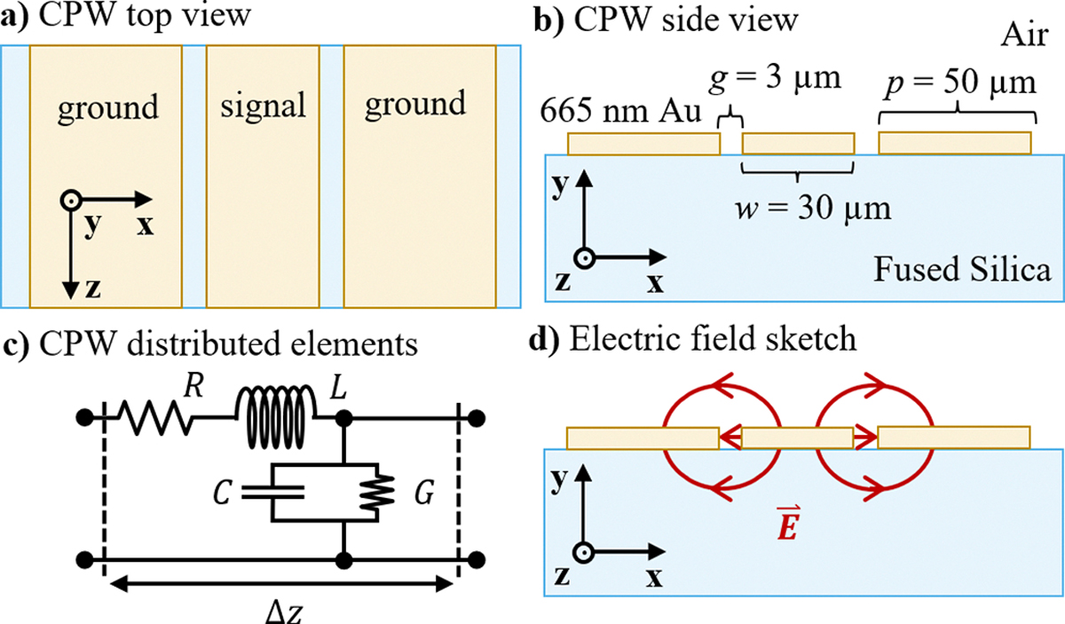
Coplanar waveguides are a type of planar transmission line. They consist of a center conductor electrode of width separated from two ground plane electrodes of width by a gap of width [Figs. 1(a) and 1(b)]. One typically represents a transmission line as a distributed circuit that consists of a resistance , inductance , capacitance , and conductance 20 [Fig. 1(c)] per unit length. These circuit parameters describe how current and voltage propagate along a transmission line. Applying Kirchhoff’s laws to a transmission line, one can derive a characteristic impedance and a propagation constant that describe the distributed attenuation and phase shift,
| (1) |
| (2) |
FIG. 1.

The coplanar waveguide (a) top view, (b) cross-sectional view, (c) representation as a transmission line with distributed resistance R, inductance L, capacitance C, and conductance G, and (d) cross-sectional sketch of the electric field penetrating the substrate.
For better readability, Eqs. (1) and (2) omit the explicit frequency dependence of each circuit parameter. CPWs support a quasi-TEM-mode [Fig. 1(d)]. In this quasi-TEM limit, and depend on the geometry of the electrodes, the conductor properties of the electrodes, and the magnetic properties of the substrate. Conversely, and depend on the geometry of the electrodes and the local dielectric environment (i.e., the substrate permittivity).
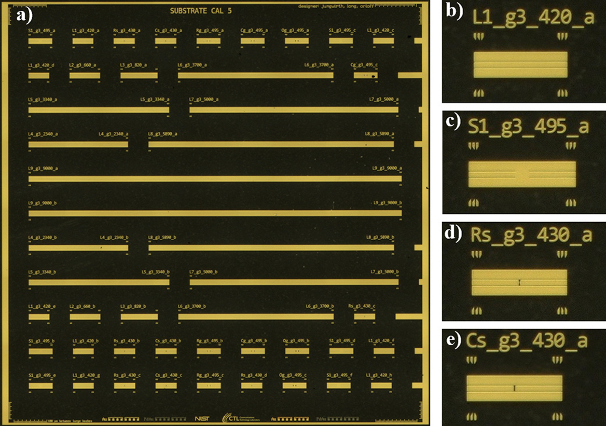
We fabricated CPW transmission lines on a 76.2 mm diameter JGS2 fused silica wafer with conventional lithographic techniques and electron-beam vapor deposition. The electrodes were nominally 500 nm thick gold with a 10 nm titanium adhesion layer. Our chip layout [Fig. 2(a)] includes a set of CPW transmission lines with lengths , and 9.000 mm [Fig. 2(b)] and a short-circuit reflect [Fig. 2(c)] to perform the multiline thru-reflect-line (mTRL) algorithm.21 Our layout includes a series resistor [Fig. 2(d)] fabricated from a PdAu alloy, which is used to estimate the capacitance per unit length22 of the CPW lines. Finally, we include a series capacitor to estimate the parasitic admittances in the series resistor compact circuit model22 [Fig. 2(e)]. We optimized our cross-sectional geometry with a small gap width (3 μm) and small ground planes (50 μm) for the frequencies up to 325 GHz.
FIG. 2.

The chip layout: (a) full view of a die and close views of (b) the thru, (c) the short-circuit reflect, (d) the series resistor, and (e) the series capacitor.
We contacted each CPW device with ground-signal-ground probe tips and measured S-parameters with a vector network analyzer. Beyond measuring S-parameters of the devices, our technique requires some additional measurements. These measurements include the physical dimensions of the CPW cross-sectional geometry and the dc-resistivity of the electrodes. We first measured the lateral dimensions of the center conductor, gaps, and ground plane widths with optical microscopy, which confirmed the nominal lateral geometry within a tolerance of 1 μm. We determined the conductor thicknesses with stylus profilometry. Our conductors were (665 ± 15) nm thick. We measured current and voltage with a source measure unit to extract the center conductor dc-resistance of each CPW. We fit the resistance of each CPW vs their lengths to extract the dc-resistance per unit length of the center conductor, .
We used the mTRL algorithm to determine the propagation constant and its uncertainty based on the measured S-parameters.21 We performed 2D finite-element field simulations of the CPW cross section to extract the distributed resistance and inductance and for the given cross-sectional geometry using the resistivity determined from dc measurements. Combining these results, we can determine and via,
| (3) |
However, this analysis assumes that the 2D simulation of the CPW cross section provides a full description of the conductor in the measurement setup. This approximation is not complete. For instance, our 2D simulations do not include radiation, moding, or crosstalk.
We checked the validity of our assumption by comparing the simulated and to and that we obtained with the series resistor standard.22,23 Measuring the reflectivity of the series resistor allows us to estimate and at low frequencies (<~40 GHz) where the impedance of the series resistor can still be modeled as a lumped element and its value can be assumed equal to the dc measurement, ,24
| (4) |
To compare the data from the series resistor and the simulated and above 40 GHz, we assumed the substrate was nondispersive, which allowed us to set and . We averaged from Eq. (4) between 1 and 10 GHz to get and used the standard deviation of as the uncertainty. Together with , we obtain and ,
| (5) |
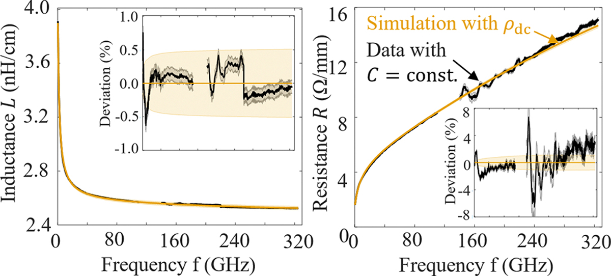
We compared and to and [Figs. 3(a) and 3(b)].
FIG. 3.

Distributed resistance L (a) and inductance R (b): comparison of the cross-sectional simulation and the data extracted from the propagation constant while assuming G = 0, C = constant.
In the 2D simulation of the CPW cross section, we implemented the conductor thickness as measured by stylus profilometry. For the lateral conductor dimensions, we used a semiempirical approach that tuned an offset () in the lateral dimensions in simulation to match R and L below 10 GHz. Heuristically, this offset represents the over- or under-development of the photoresist and corrects the nominal geometry to the physical geometry,
| (6) |
We obtained an over-development of , producing , and . This approach to the lateral dimensions proved more self-consistent with the impedance computed by a series resistor than microscope images alone. We used the -corrected dimensions and the measured distributed dc-resistance to obtain a conductor resistivity of , which is comparable to other reports of electron-beam-deposited gold.25 Using a single parameter to capture the dimensional uncertainty due to fabrication process variation simplified the error analysis and more realistically captured the effect of over or under developing the photoresist. Finally, we used 2D simulations of the CPW cross section with the -corrected dimensions to extract the permittivity from the distributed capacitance [Fig. 4(a)],
FIG. 4.

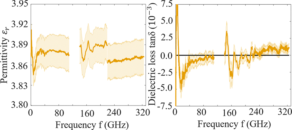
The complex permittivity of fused silica extracted from and the simulated and : (a) real permittivity and (b) loss tangent.
The first term is negative because the air above the CPW also contributes to . We used the relation to extract the dielectric loss tangent [Fig. 4(b)].
We evaluated our results for the CPW in distributed resistance , distributed inductance [Figs. 3(a) and 3(b)], and substrate permittivity and dielectric loss [Figs. 4(a) and 4(b)]. The simulated and both agreed with extracted and within the measurement uncertainty. This agreement supports that the skin effect dominates the frequency trend of and over the whole measured range.26 More interestingly, we conclude that the effect of the dielectric slab mode is negligible, even though most of our measured band is above its critical frequency for our thick fused silica substrate.27 Hence, we conclude that our 2D simulation of the CPW cross section is indeed appropriate, and we proceeded with our evaluation based on and .
Using the simulated and and the extracted from the measured S-parameters, we obtained permittivity and dielectric loss. The extracted permittivity with the respective standard uncertainty is comparable to previous measurements at lower frequencies12 and from optical setups.16 However, fused silica’s permittivity varies with the manufacturing process,9,10 which makes our result representative of what one might expect rather than a sampling of all possible materials. A rigorous comparison of different methods for the same wafer is under way. More interestingly, our measurement is consistent with a dielectric loss over the whole frequency range and is consistent with the approximation that the for most applications. While we do not observe any significant dispersion of the permittivity and our results are consistent with a constant permittivity over the whole frequency range, it is possible that there are loss mechanisms within our uncertainty. By far the biggest contribution to the uncertainty of the permittivity extraction is the systematic uncertainty in the -corrected determination of the lateral geometry of the CPW, which we estimated to be in the fit. The uncertainty in is systematic over the whole frequency range and does not place caveats on our observation that JGS2 fused silica is effectively dispersionless. From a set of three calibrations up to 110 GHz, we estimate the repeatability in the extracted permittivity to be better than 0.5%.
Nonetheless, there are some things we are still working to understand and are the subject of ongoing research. For instance, we attribute the deviations around 160 GHz to an imperfect probe contact rather than an actual dispersion of the substrate permittivity because the imaginary and real parts of the permittivity do not physically relate to each other (i.e., they do not follow Kramers–Kronig relations). The compression in the samplers on the VNA extender heads is another alternative explanation for the peak near 160 GHz. There is also an unphysical dip in the permittivity and the loss around 10 GHz, which is inconsistent with other measurements of the same fused silica with different electrode geometries designed to work at lower frequencies. At present, we think these inconsistencies may indicate systematic errors due to the chosen geometry of our devices rather than the metrology itself. We optimized the geometry for high frequencies, which decreases the lateral dimensions of the CPW to reduce radiation. We suppose that the smaller dimensions and resulting increased conductor loss may imply that it is more difficult to distinguish the dielectric losses from conductor losses. In addition, the chosen geometry is close to limits of our maskless lithography tool (~1 μm), which may have resulted in lithography artifacts that could have a stronger impact than anticipated. Taken together, these results suggest a future study that explores process variation and some comparisons between lithographic techniques. Taking into account the systematic deviations of the geometry in this work, we claim a resolution on the loss tangent above 1 GHz with this geometry (Fig. 4b). Nevertheless, the key result is that this technique provides an extremely broadband technique to observe that fused silica may be considered both dispersion- and lossless for many practical on-wafer applications up to 325 GHz.
In conclusion, the objective of this work was to test an on-wafer approach to extract the complex permittivity of fused silica up to 325 GHz. We chose fused silica because it is a candidate for mmWave applications and there has been a material property measurement gap for frequencies above 110 GHz. Importantly, our measurements used a form factor that is analogous to the end-use applications in 6G electronics, producing data that more closely replicates what others might encounter in mmWave devices. We used 2D simulations to model the conductor properties and extracted the propagation constant of our CPW transmission lines from their S-parameters with the multiline thru-reflect-line algorithm. Our extracted permittivity is consistent over all three measured frequency bands and comparable to previous measurements. As we do not observe any relevant dispersion, we conclude that for most technical applications fused silica can be assumed dispersionless up to 325 GHz. Furthermore, our findings show that it is the Ohmic loss in the conductor that dominates the power loss in CPW transmission lines on fused silica, even at frequencies as high as 325 GHz. In summary, our results support choosing fused silica as basis for semiconductor manufacturing of next-generation communications technology up to 325 GHz.
Acknowledgments
The authors thank the critical review of L. Enright, C. Yung, and J. C. Booth, all with the National Institute of Standards and Technology (NIST), for their critical feedback during this research, and their comments on this paper’s manuscript. This paper is an official contribution of NIST, not subject to copyright in the US. Usage of commercial products herein is for information only; it does not imply recommendation or endorsement by NIST. The data that support the findings of this study are available from the corresponding author upon reasonable request.
Footnotes
Conflict of Interest
The authors have no conflicts to disclose.
DATA AVAILABILITY
The data that support the findings of this study are available from the corresponding author upon reasonable request.
REFERENCES
- 1.Orloff ND, Ubic R, and Lanagan M, “Special topic on materials and devices for 5G electronics,” Appl. Phys. Lett. 120(6), 060402 (2022). [Google Scholar]
- 2.Cai L, Wu J, Lamberson L, Streltsova E, Daly C, Zakharian A, and Borrelli NF, “Glass for 5G applications,” Appl. Phys. Lett. 119(8), 082901 (2021). [Google Scholar]
- 3.Nelson SF, Levy DH, and Shorey AB, in IEEE 70th Electronic Components and Technology Conference (ECTC) (IEEE, Orlando, FL, 2020), pp. 1986–1991. [Google Scholar]
- 4.Shorey A, Nelson S, Levy D, and Ballentine P, in 53rd International Symposium on Microelectronics (IMAPS, 2020), pp. 192–196. [Google Scholar]
- 5.Shorey A, Nelson S, Levy D, and Ballentine P, in 52nd International Symposium on Microelectronics (IMAPS, 2019), pp. 147–151. [Google Scholar]
- 6.Levy DH, Nelson SF, Shorey AB, and Balentine P, in IEEE 71st Electronic Components and Technology Conference (ECTC) (IEEE, San Diego, CA, 2021), pp. 2222–2228. [Google Scholar]
- 7.Letz M, in IEEE MTT-S International Microwave Workshop Series on Advanced Materials and Processes for RF and THz Applications (IMWS-AMP) (IEEE, Bochum, Germany, 2019), pp. 85–87. [Google Scholar]
- 8.Letz M, Engelmann H, Lautenschlager G, Brune N, Bai X, Salski B, and Karpisz T, in 51st European Microwave Conference (EuMC) (IEEE, London, UK, 2022), pp. 103–106. [Google Scholar]
- 9.Rodriguez-Cano R, Perini SE, Foley BM, and Lanagan M, “Broadband characterization of silicate materials for potential 5G/6G applications,” IEEE Trans. Instrum. Meas. 72, 6003008 (2023). [Google Scholar]
- 10.Li L, Fang Y, Xiao Q, Wu YJ, Wang N, and Chen XM, “Microwave dielectric properties of fused silica prepared by different approaches,” Int. J. Appl. Ceram. Technol. 11(1), 193–199 (2014). [Google Scholar]
- 11.Salski B, Cuper J, Karpisz T, Kopyt P, and Krupka J, “Complex permittivity of common dielectrics in 20–110 GHz frequency range measured with a Fabry–Pérot open resonator,” Appl. Phys. Lett. 119(5), 052902 (2021). [Google Scholar]
- 12.Janezic MD and Krupka J, “Split-post and split-cylinder resonator techniques: A comparison of complex permittivity measurement of dielectric substrates,” J. Microelectron. Electron. Packag. 6(2), 97–100 (2009). [Google Scholar]
- 13.Baker-Jarvis J, Geyer RG, Grosvenor JH, Janezic MD, Jones CA, Riddle B, Weil CM, and Krupka J, “Dielectric characterization of low-loss materials a comparison of techniques,” IEEE Trans. Dielect. Electr. Insul. 5(4), 571–577 (1998). [Google Scholar]
- 14.Janezic MD, Kuester EF, and Jarvis JB, in IEEE MTT-S International Microwave Symposium Digest (IEEE, 2004), pp. 1817–1820. [Google Scholar]
- 15.Arz U, Kuhlmann K, Dziomba T, Hechtfischer G, Phung GN, Schmuckle FJ, and Heinrich W, “Traceable coplanar waveguide calibrations on fused silica substrates up to 110 GHz,” IEEE Trans. Microwave Theory Techn. 67(6), 2423–2432 (2019). [Google Scholar]
- 16.Chen S, Nguyen K, and Afsar M, in European Microwave Conference (IEEE, Manchester, UK, 2006), pp. 384–387. [Google Scholar]
- 17.Afsar MN and Button KJ, “Millimeter-wave dielectric measurement of materials,” Proc. IEEE 73(1), 131–153 (1985). [Google Scholar]
- 18.Enright L, Olszewska-Placha M, Hill M, Phommakesone S, Kato D, Hill CA, Kähäri H, Lee C, Chen C-S, Orloff ND, Celuch M, and Ray U, in International Conference on Electronics Packaging (ICEP) (IEEE, Kumamoto, Japan, 2023), pp. 1–2. [Google Scholar]
- 19.See https://www.inemi.org for “International Electronics Manufacturing Initiative (iNEMI) (2024).”.
- 20.Marks RB and Williams DF, “A general waveguide circuit theory,” J. Res. Natl. Inst. Stan. 97(5), 533 (1992). [DOI] [PMC free article] [PubMed] [Google Scholar]
- 21.Marks RB, “A multiline method of network analyzer calibration,” IEEE Trans. Microwave Theory Techn. 39(7), 1205–1215 (1991). [Google Scholar]
- 22.Drisko JA, Chamberlin RA, Booth JC, Orloff ND, and Long CJ, “Optimal series resistors for on-wafer calibrations,” IEEE Trans. Microwave Theory Techn. 68(1), 196–210 (2020). [Google Scholar]
- 23.Williams DF and Walker DK, in 50th ARFTG Conference Digest (IEEE, Portland, OR, 1997), pp. 131–137. [Google Scholar]
- 24.Williams DF and Marks RB, “Transmission line capacitance measurement,” IEEE Microwave Guid. Wave Lett. 1(9), 243–245 (1991). [Google Scholar]
- 25.Sambles JR, Elsom KC, Jarvis DJ, and Blackman M, “The electrical resistivity of gold films,” Philos. Trans. R. Soc., A 304, 365–396 (1982). [Google Scholar]
- 26.Wheeler HA, “Formulas for the Skin effect,” Proc. IRE 30(9), 412–424 (1942). [Google Scholar]
- 27.Spirito M, Arz U, Phung GN, Schmückle FJ, Heinrich W, and Lozar R, “Guidelines for the design of calibration substrates, including the suppression of parasitic modes for frequencies up to and including 325 GHz: EMPIR 14IND02,” (2018). [Google Scholar]
Associated Data
This section collects any data citations, data availability statements, or supplementary materials included in this article.
Data Availability Statement
The data that support the findings of this study are available from the corresponding author upon reasonable request.


