Abstract
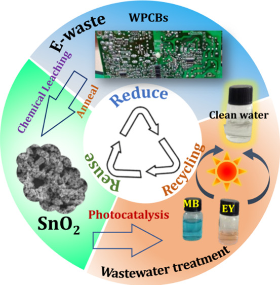
Electronic waste (e-waste) has become a significant environmental concern worldwide due to the rapid advancement of technology and short product lifecycles. Waste-printed electronic boards (WPCBs) contain valuable metals and semiconductors; among them, tin can be recycled and repurposed for sustainable material production. This study presents a potential ecofriendly methodology for the recovery of tin from WPCBs in the form of tin oxide nanostructured powders. The soldering points in the WPCBs are extracted and dissolved in the dilute HNO3 solution, followed by the formation of metastannic acid, which is subsequently transformed into SnO2 nanoparticles. Different characterization techniques (XRD, XPS, FE-SEM, and TEM) are employed to confirm the morphology and composition of nanoparticles. The prepared SnO2 NPs, having a size range of <50 nm, show excellent photocatalytic degradation of cationic (methylene blue, MB) and anionic (eosin Y, EY) dyes for wastewater treatment. The as-synthesized SnO2 can degrade the mixed dyes (MB+EY) under the illumination of natural sunlight at rate constants of 0.0153 and 0.1103 min–1 for MB and EY, respectively. The positive zeta potential and smaller particle size of the SnO2 NPs possess the extra advantage of the adsorption of anionic over cationic dye, resulting in faster degradation of EY, which is further supported by DFT calculation. The synthesis of SnO2 from waste-printed electronic boards offers a dual benefit: It not only provides a sustainable solution for managing electronic waste but also contributes to the production of useful photocatalysts for wastewater treatment. By converting waste into valuable resources, this approach aligns with the principles of the circular economy and mitigates the environmental impact associated with e-waste disposal.
1. Introduction
With the world’s fastest-expanding economies and populations, demand for electrical and electronic equipment (EEE) is increasing. As a result, it is directly instigating a significant amount (50–70 million tons) of electronic waste (e-waste) to be generated globally every year, and it is estimated to increase to 111 million tons per year by 2050.1−3 A considerable amount of e-waste is often exposed to informal recycling procedures or disposed of in landfills, often in violation of required environmental protocols. As a result, precious resources are depleted, and several ecological threats are posed.4,5 Therefore, proper e-waste recycling is one of the state-of-the-art processes that can compete with the problems associated with e-waste. Also, a large amount of base and precious metals can be recovered from e-waste. According to the report, 70% of e-waste is generated from compute devices, 12% from telecom sectors, and 8% from medical equipment6 and merely 17% of the total amount of e-waste generated is disposed of through formal recycling procedures.7,8 Printed circuit boards (PCBs) are one of the important components in EEE that contribute 6 wt % of the total e-waste created globally and expected to grow at a compound annual growth rate of 3.50% during 2023–2030.9 PCBs contains metallic elements such as Cu (12–29%), Sn (1.1–4.8%), Pb (1.3–3.9%), Fe (0.1–11.4%), and Zn (0.1–2.7%) and precious metals like Au (0.0029–0.112%) as well as ∼49% ceramic material and ∼23% plastic, although the actual percentage varies with different classes of PCBs.10,11 So PCBs that comprise both precious and base metals can be regarded as a significant secondary source of valuable metals. Among the different metals found in PCBs, more than 65% tin (95% for Pd-free) was used in solder for connections between elements and tracks on the board.12 However, tin is a relatively scarce element with an abundance in the earth’s crust of about 2 ppm.13,14 Therefore, recovering tin from e-waste would be a beneficial and secondary source for tin compared with traditional mining approaches.
Creating new, useful, marketable goods from waste may be essential to achieving desired products. Different recycling techniques have been used to extract various types of nanomaterials from electronic trash, such as metals (copper, silver, gold, palladium, lead, and tin) and metal oxides (copper oxide, cuprous chloride, copper ferrite, lead oxide, tin oxide, and silicon carbide).15
Metal oxides extracted from electronic waste possess diverse applications, including photocatalysis, supercapacitor materials, and sensors, as reported in several research papers.16−20 Tin oxide (SnO2) is one of the novel n-type semiconductor photocatalysts that gained attention because of its large amount of applications in different fields like catalysis,21 electrocatalytic anodes,22 gas sensing,23,24 optoelectronic devices,25,26 field emission displays,27 humidity sensing,28 dye based-solar cells,29 coatings,30 light-emitting diodes,31 and supercapacitors.32 Different methods such as sol–gel,33 chemical vapor deposition (CVD),34 coprecipitation,35 and hydrothermal method36 were used to synthesize SnO2. Due to its wide bandgap value (3.6 eV), it displays good photocatalytic behavior toward sunlight absorption.37−39
Based on the production processes, industries such as textile and pharmaceuticals generate a lot of contaminants and release the waste into the freshwater. For example, the textile sector produces wastewater containing a variety of dyes. Because of their complex chemical structures, these dyes are extremely stable in ambient conditions, and removal or degradation from effluents is difficult. It directly affects humans or other animals in the environment.40 Different remedial approaches, such as chemical, biological, and physical have been performed.41,42 For decades, photocatalysts have significantly reduced the hazardousness of organic dyes by degrading them into a nonharmful or less hazardous state.43 In this direction, Nascimento et al. showed WPCBs to create polymetallic NPs, including Cu, Zn, Ni, and Fe, which were then used to degrade reactive blue 4 (RB4).44 Khayyam Nekouei et al. investigated methylene blue (MB) removal via direct transformation of WPCBs and reported that 92% of MB was destroyed after 450 min of UV irradiation.45
In the present study, waste PCBs are used as the source of Sn (focusing on the importance of e-waste recycling) to prepare a novel SnO2 nanoparticle for the photodegradation of mixed cationic and anionic dye molecules such as MB and EY, respectively. The solder alloy (Sn and Pb) was collected from WPCBs and treated with concentrated nitric acid to form metastannic acid, followed by SnO2 nanoparticles. The product was characterized using XRD, SEM, TEM, XPS, UV-DRS, and EDS techniques. Later, SnO2 nanoparticles are used as photocatalysts for individual water pollutants (MB, EY, and MB+EY) degradation under direct sunlight, and the process is investigated by a DFT study.
2. Experimental Section
2.1. Preparation of SnO2 Nanoparticles
All of the waste PCBs were collected from our institute. First, the WPCBs were washed with soap water to remove the dirt, followed by sonication in a water/ethanol mixture. Later, the WPCBs were dried in a vacuum oven at 60 °C for overnight. To recover the tin (Sn) from the WPCBs, the soldering points were desoldered manually and separated. Then, the desoldered materials were treated with 5 M HNO3 solution at room temperature with constant stirring (∼400 rpm) overnight. During the leaching process, except Sn, other metals present in the soldered points were dissolved in HNO3 solution and Sn reacted with HNO3 to form a white precipitate in the form of Meta stannic acid (H2SnO3), shown in eqs 1 and 2.46,47
| 1 |
| 2 |
The white solution was centrifuged and washed with distilled water several times. The precipitate was dried under ambient conditions. Later, the white precipitate was mixed with 200 mg of sucrose and transferred to the muffle furnace for 2 h at 800 °C. The faded-yellow product was washed with a water and ethanol mixture and dried in an oven at 60 °C overnight. Finally, SnO2 nanoparticles were formed using eq 3:
| 3 |
2.2. Characterization
The crystallinity, crystallite size, and crystal structure of the synthesized SnO2 NPs were evaluated by the powder X-ray diffraction (XRD) method using a Rigaku Ultima X-ray powder diffractometer with Cu Kα radiation of wavelength 1.5418 Å. The structural features and morphology were confirmed by field emission scanning electron microscopy (FE-SEM) and transmission electron microscopy (TEM; JEOL 200 kV) equipped with energy-dispersive X-ray spectroscopy (EDS) analysis. The optical absorbance property was obtained by ultraviolet–visible diffuse reflectance spectroscopy (UV-DRS) spectra using a Shimadzu spectrophotometer at the range of 200 to 800 nm. The Raman spectroscopy of the catalyst was measured in a confocal Raman spectrophotometer using a HORIBA Jobin Yvon LabRAM Raman microscope with an excitation wavelength of a 532 nm Ar+ laser as a source. X-ray photoelectron spectroscopy (XPS) measurements were carried out using a Thermo Fisher K-Alpha instrument with an Al Kα X-ray source (1486.6 eV). The stability of the SnO2 particles was analyzed with a zeta potential analyzer (Malvern Panalytical).
2.3. Photocatalytic Degradation
The photocatalytic efficiency of the SnO2 catalyst was demonstrated by the degradation experiment of cationic MB dye and anionic eosin yellow (EY) using direct sunlight. A 100 mL solution of MB and EY dyes was taken from stock solution (1 × 10⁻⁵ M) into a 250 mL reaction bottle and treated with 0.5 g L–1 of SnO2 catalyst. The solution was stirred for 30 min in the dark to attain absorption and desorption equilibrium before being exposed to sunlight. The experiment was carried out during daytime from 10 a.m. to 4 p.m. at Kancheepuram district, Tamil Nadu (state), India, with an average light intensity of ∼680–700 W/m2.48 At regular time intervals (1 h for MB and 10 min for EY), 4 mL of sample aliquot was collected and centrifuged at 4000 rpm for 5 min for absorption studies. The absorption spectra were collected using a UV–visible spectrophotometer (PerkinElmer UV–vis Lambda 35). Photocatalytic degradation (PD) efficiency was calculated using eq 4:49
| 4 |
where Co represents the initial absorbance and Ct is the final absorbance of the dye solution before and after the light illumination at a time t, respectively.
The first-order reaction rate constant (k) was calculated using eq 5:
| 5 |
3. Results and Discussion
3.1. Structural Study
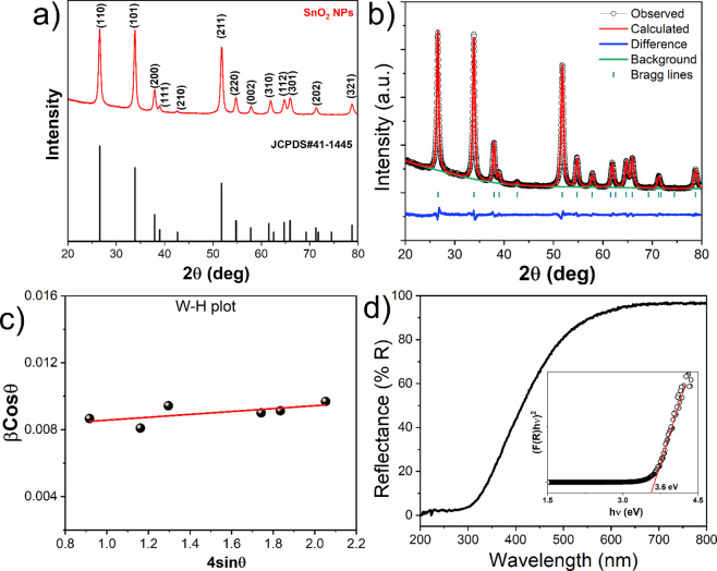
The synthesized SnO2 NPs are subjected to XRD analysis to determine their crystalline nature and phase purity, as shown in Figure 1a. All the diffraction peaks in the XRD pattern correspond to the rutile structure and crystallize in the tetragonal P42/mnm space group, which is further confirmed by JCPDS card no. 41-1445. The XRD patterns of the as-synthesized SnO2 NPs are refined (Figure 1b) using the Profex refinement approach to check the phase purity and ascertain the structural characteristics. The values of structural parameters such as crystal system, space group, lattice constant, χ2, and goodness of fit (GoF) are listed in Table 1. The lattice parameter values of a = 4.737 and c = 3.186 Å, correspond to the same JCPDS card no. as shown in Table 1.
Figure 1.
(a) XRD pattern of as-synthesized SnO2 NPs compared with JCPDS card no. 41-1445. (b) Rietveld refinement profile obtained from the powder diffraction pattern of SnO2 NPs. (c) Willamson–Hall plot for SnO2 NPs. (d) UV-DRS of SnO2 NPs synthesized from E-waste (the inset shows the Kubelka–Munk plot for direct band gap (3.6 eV) energy calculation).
Table 1. Rietveld Refinement Parameters Obtained for SnO2 NPs.
| crystal structure | space group | lattice constant | χ2 | GoF | |
|---|---|---|---|---|---|
| SnO2 NPs | rutile tetragonal | P42/mnm | a = 4.7386 Å | 1.8 | 1.34 |
| c = 3.186 Å | |||||
| crystallite size (D) | microstrain (ε) | dislocation density (δ = 1/D2) | |||
| 17.8 nm | 0.86 × 10⁻³ | 0.0038 nm–2 | |||
The broadening of the XRD peaks is related to the small crystallite size and microstrain present in the crystal structure, and the values can be determined using the Williamson and Hall (W–H) plot, as shown in eq 6:
| 6 |
where β is the full width half maxima of the XRD peak, k is the Scherrer constant, λ is the wavelength of Cu Kα radiation, and θ is the angular position of each XRD peak.
The W–H plot, which is derived from eq 6, is illustrated in Figure 1c. The crystallite size and microstrain are determined to be 17.8 nm and 0.86 × 10⁻³, respectively, by utilizing the intercept and slope of the linear equation (y = mx + c; y = βcosθ, x = sinθ). The results are listed in Table 1. The dislocation density, or the number of dislocations per unit volume of the SnO2 crystal, was determined to be 0.0038 nm–2. The obtained values are comparable to the SnO2 materials synthesized by different methods.50,51
To determine the optical band gap of synthesized SnO2, the UV-DRS technique was employed and the graph is shown in Figure 1d. The spectrum of the SnO2 nanoparticles shows a rapid decrease after 400 nm, related to the optical absorption edge of the material.52 To determine the precise value of the optical band gap of SnO2, the reflectance values were converted to absorbance by application of the Kubelka–Munk function53 using eq 7:
| 7 |
where R is the reflectance and F(R) is the Kubelka–Munk function, respectively.
After that, the band gap value was interpreted directly using eq 8:
| 8 |
where A is a constant for the semiconductor material, hν is the photon energy, and Eg is the optical band gap value. By extrapolating the linear region of the graph to the energy axis, the band gap value of SnO2 NPs is found to be 3.6 eV (inset of Figure 1d), which is comparable to the literature data.37
The detailed top view of the as-synthesized SnO2 NPs from E-waste was investigated using FE-SEM and is depicted in Figure 2a,b at different magnifications. Anisotropic nanoparticles of SnO2 were found at lower (Figure 2a) and higher (Figure 2b) magnifications from the top view of the FE-SEM image. Particle clustering appears to have occurred on the surface.
Figure 2.
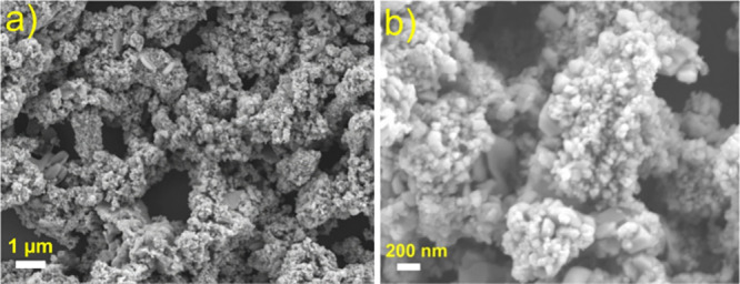
FE-SEM images of SnO2 NPs at lower (a; scale bar = 1 μm) and higher magnifications (b; scale bar = 200 nm).
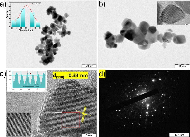
Figure 3a,b presents the bright-field TEM images of the as-synthesized SnO2 nanoparticles. The average size of the SnO2 nanoparticles (inset of Figure 3a) is found to be ∼35 nm. From the higher magnification BF image (Figure 3b), it is evident that as-synthesized SnO2 possesses a platelet-like morphology (inset Figure 3b). The HRTEM image of SnO2 nanoparticles with a well-defined lattice pattern in Figure 3c reveals their crystalline character, which is required for successful photoinjected charge transport. As seen in the inverse FFT of HRTEM image, the SnO2 nanoparticles possess lattice fringes (inset Figure 3c) with an interplanar distance (d-spacing) of 0.33 nm that can be indexed as the (110) plane. The SAED pattern of the SnO2 NPs is shown in Figure 3d, and it is clear from the bright spots that the SnO2 particles are crystalline.
Figure 3.
(a) Bright-field TEM image of as-synthesized SnO2 NPs (scale bar = 100 nm) at low magnification and (b) high magnification (scale bar = 50 nm); the particle size distribution histogram is shown in the inset of (a). The single nanoparticle is displayed in the inset of (b). (c) HRTEM image of SnO2 NPs; inverse FFT of the selected region (red color) of the HRTEM image; the inset shows the line profile for the selected line in its inverse FFT image indicating its d spacing as 0.33 nm. (d) SAED pattern of SnO2 NPs.
EDX is considered for analyzing the elemental composition of the solid sample. Focusing on different areas of the sample, EDX was performed using a copper TEM grid to confirm the spontaneous presence of Sn and oxygen (O). Both tin and oxygen are homogeneously dispersed in the sample depicted from the elemental mapping of Sn and O in Figure S1. The atomic percentages of elemental tin and oxygen were determined from the EDX analysis, revealing tin and oxygen contents of 40 and 60%, respectively. The absence of peak of carbon (C) in the EDX spectrum suggests that sucrose was used as the fuel for synthesis and was not included in the catalyst.
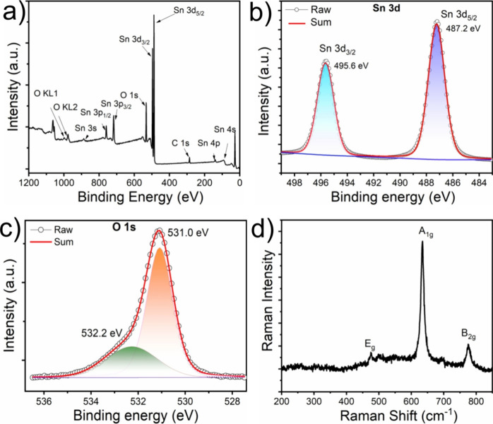
The surface chemistry and chemical composition of the as-synthesized SnO2 obtained from XPS is presented in Figure 4. The survey XPS spectrum of SnO2 is depicted in Figure 4a. The spectrum exclusively identifies carbon, oxygen, and tin; no other elements are detected. The peaks of Sn 3d, 4d, 3p, 4p, and 4s from SnO2 are observed. As shown in Figure 4b, the high-resolution XPS spectrum of Sn 3d exhibits two peaks, Sn 3d3/2 and 3d5/2 with binding energies of 495.6 and 487.2 eV, respectively, due to the spin–orbit coupling of the Sn4+ oxidation state in SnO2. Figure 4c illustrates the high-resolution O 1s XPS spectrum of SnO2, where the deconvoluted oxygen spectra appear in two chemical states at 531.0 and 532.2 eV, respectively. The first peak is related to Sn–O/Sn–O–Sn bonds, and the second one is associated with nonlattice oxygen adsorption in the form of hydroxyl groups. The change in the peak intensities is attributed to the variation of OH groups on the catalyst’s surface.54
Figure 4.
XPS spectra of SnO2 nanoparticles; (a) survey spectrum of SnO2; (b) high-resolution Sn 3d XPS spectrum, (c) high-resolution O 1s XPS spectra; (d) Raman spectrum of SnO2 nanoparticles.
Raman spectroscopy was used to further investigate the crystal structures of SnO2 nanoparticles. The point group of rutile SnO2 is known as D4h. According to the point group, there are 18 vibrational modes; among them, doubly degenerate Eg and nondegenerate A1g, B1g, and B2g are the Raman active modes.55 As shown in Figure 4d, the Raman spectra of the synthesized SnO2 contain three peaks at 475, 634, and 775 cm–1. The Raman band at 475 cm–1 assigned to the Eg mode possesses the vibration of oxygen and 775 cm–1 to the B2g mode. The Raman band at 634 cm–1 attributed to the A1g mode represents the symmetric stretching of Sn–O bond vibration and is the most intense band among Eg, A1g, and B2g. These Raman peak positions are well matched with the reported values at 476 cm–1 (Eg), 635 cm–1 (A1g), and 776 cm–1 (B2g) for the rutile structure of the SnO2 sample with a tetragonal matrix.56,57
3.2. Photocatalytic Dye Degradation
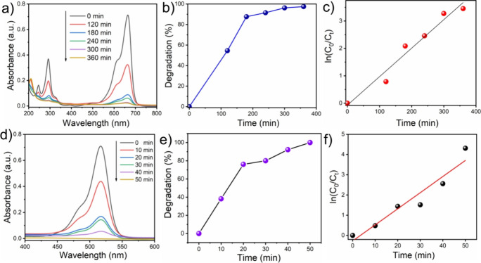
The removal and photocatalytic degradation of dye pollutants by the as-synthesized SnO2 catalyst was qualitatively investigated using a model cationic and anionic dye (at pH ∼ 7) such as MB and EY, respectively. At first, the SnO2 catalyst was dispersed in the MB dye solution (10–5 M) and kept for 30 min under dark conditions to attain the dye adsorption equilibrium. Then, the sample bottle was subjected to keeping under natural sunlight (680–700 W/m2) for a few hours, and the photocatalytic degradation of MB was analyzed. All the data were collected three times (Figure S2), and only the average data points are shown in the plot. Figure 5a shows the changes in the UV–vis spectra during MB photodegradation under sunlight. The absorption peaks with a shoulder between 600 and 700 nm are assigned to the absorption of the heteropolyaromatic linkage of MB, while the peaks close to 300 nm correspond to the absorption of the phenothiazine ring—a polycyclic aromatic structure. The intensity of the maximum absorption peak of 664 nm decreases gradually as the sunlight irradiation time increases, indicating the photocatalytic degradation of the MB dye in the presence of SnO2 catalyst.
Figure 5.
(a) UV–vis absorption spectra of degradation of MB with SnO2 NPs under sunlight irradiation as a function of time. (b) Photocatalytic % of degradation with time for MB solution. (c) Kinetic relationship of ln(Co/Ct) vs irradiation time curve for MB solution (R2 = 0.964). (d) UV–vis adsorption spectra of degradation of EY solution with SnO2 NPs under sunlight irradiation as a function of time. (e) Photocatalytic % of degradation with time for EY solution. (f) Kinetic relationship of ln(Co/Ct) vs irradiation time curve for EY solution.
From Figure 5b, it is observed that approximately 87% of the dye is photodegraded after irradiation of 180 min and further illumination up to 360 min; ∼97.1% of the MB dye is degraded. The near-flattering absorption peaks in the UV–vis spectrum imply that conjugation in the heterocyclic structure is disturbed or might be broken during sunlight irradiation. The decolorization process and the conjugate structure collapse essentially happened at the same time. The two other peaks, at 292 and 246 nm, similarly fell concurrently with the most intense peak, suggesting that hydroxyl radicals attacked the phenothiazine structure and benzene, oxidizing and opening the ring.58 In summary, a shift in dye concentration under dark conditions suggests that dye molecules are physically transferred from the solution to the surface of the adsorbent. Superoxide and hydroxyl radicals are produced by the semiconductor’s production of photo charge carriers (photoelectron and photo hole) at the valence band and conduction band, respectively, under light illumination.59,60 In a nutshell, the photogenerated electrons and holes react in a similar manner found in literature.61
To further illustrate the photocatalytic ability of the SnO2 catalyst toward MB dye, the experimental data was subjected to the Langmuir–Hinshelwood kinetic model. The ln(Co/Ct) versus irradiation time is plotted (Figure 5c) based on eq 5 and follows a linear kinetic relationship. The reaction rate constant for the photodegradation of MB as the slope of the line (regression coefficient, R2 = 0.964) is 0.0104 min–1, which is comparable to the SnO2-based catalyst cited in the literature.62
The kinetic order of the photodegradation was verified at low initial concentrations by examining the ln(Co/Ct) vs time plot, and it is evident from the plot that photocatalytic degradation of the MB dye follows the first-order kinetics as the correlation constant (R2) for the fitted line is found to be greater than 0.95 (0.964).
To understand the photocatalytic degradation activity of MB using as-synthesized SnO2, commercial SnO2 nanoparticles (TCI Chemicals, 99.5%) and SnO2 prepared by conventional methods (hydrothermal)63 are compared and shown in Figure S3. It was shown that the SnO2 as synthesized from WPCBs is nearly equal to the commercial SnO2 particles and degrades the MB dye faster than does SnO2 from the conventional method.
Similarly, photocatalytic degradation of EY (10–5 M) was carried out by using SnO2 nanoparticles under sunlight. Before irradiation, the photocatalytic mixture was kept for 30 min under dark conditions to attain the dye adsorption equilibrium. The intensity of the maximum absorption peak (517 nm) for EY decreased rapidly over time (Figure 5d). After 20 min of sunlight exposure, approximately 75% of the dye is degraded. Within 50 min, the UV–visible spectra (Figure 5d) align with the x-axis, indicating ∼100% degradation of EY. The percentage of degradation vs time graph in the presence of the SnO2 catalyst and sunlight is displayed in Figure 5e. Similarly, the photocatalytic ability of the SnO2 catalyst toward the EY dye is investigated and ln(Co/Ct) versus irradiation time is plotted (Figure 5f). It was found that the photodegradation of EY follows pseudo-first-order kinetics (R2 = 0.924 < 0.95) and the rate constant of EY is found to be 0.0796 min–1.
It is observed from the experiments described above that EY degrades faster than MB by keeping other parameters constant. To understand the interaction of MB and EY on the surface of the NPs, the zeta potential of SnO2 was recorded and are displayed in Figure S4. The zeta potential value for SnO2 nanoparticles is 11.5 mV, indicating an inherently positively charged surface that can strongly attract the negatively charged dye molecules than positively charged dye.
The efficacy of dye pollutant remediation is further validated in a mixed dye solution containing two distinct dyes, MB and EY, respectively. An optical absorbance spectrum of the mixed dye solution with time was acquired and is depicted in Figure 6a, where two distinct absorption maxima were observed at 664 and 516 nm for individual MB and EY, respectively. As anticipated, the SnO2 catalyst effectively eliminated 100% of anionic dye, i.e., EY, and 77% of cationic dye, i.e., MB, from the mixed dye solution upon 60 min of irradiation by sunlight. We observed that in a mixed dye solution, MB shows faster degradation than the individual, and within 180 min of sunlight illumination, it attains 95% degradation. This describes that the as-synthesized photocatalyst exhibits a strong affinity toward anionic dye. It can be speculated that negatively charged EY adsorbs on the positively charged SnO2 surface better than positively charged MB dye. As a result, EY has greater access to the photo charge carrier than MB, leading to faster degradation. Figure 6b shows the Ct/Co vs irradiation time plot, and it exhibits that EY dye photo degraded exponentially with time, whereas MB dye degraded slowly. The ln(Co/Ct) vs time (Figure 6c) plot shows that both dyes follow the pseudo-first-order kinetics, and rate constants for MB and EY are found to be 0.0153 and 0.1103 min–1, respectively. The visible increment of the rate constant for MB in the mixture was the result of the reduction of the electrostatic repulsion between MB and the catalyst.
Figure 6.
(a) UV–vis absorption spectra of degradation of MB and EY with SnO2 NPs under sunlight irradiation at different time intervals. (b) Relative concentration (Ct/Co) vs time plot of MB and EY in mixed dye solution. (c) Kinetic relationship of ln(Co/Ct) vs irradiation time curve for mixed dye (MB and EY) solution.
Under real sunlight conditions, the photothermal effect naturally becomes an integral part of photocatalytic processes due to the broad spectrum of sunlight, which includes not only the ultraviolet (UV) and visible-light regions but also the infrared (IR) region. The photothermal effect also depends on the nature of the dye molecules. To understand the photothermal effect on the photocatalytic process, a set of experiments was performed where two mixed dye solutions were kept under the sunlight with and without catalyst (SnO2), and it was found that the absorbance value (Figure S5) for MB decreased a little (0.44 to 0.41) compared to EY (0.71 to 0.41). However, in the presence of a catalyst, the absorbance values for MB and EY reached 0.37 and 0.11, respectively. This clearly reveals that the photothermal effect has little contribution (on the nature of the dye) in the photocatalytic dye degradation.
Reusability serves as a measure to assess the stability and efficiency of the catalyst. Before being reused, the SnO2 catalyst was cleaned three times with water, and then with ethanol, and dried in a hot air oven at 300 °C for 3 h. Photocatalytic studies were repeated utilizing the recovered catalyst, and there was no significant difference in the % degradation of MB and EY in their single solution after the third consecutive cycle (Figure S6). Such reusability of the SnO2 catalyst clearly defines the efficiency and hence confirms its outstanding performance. To verify the crystal structure and chemical composition of SnO2 after recycling, the material was tested using XRD and XPS and is shown in Figure S7. No changes in peak position for both XRD and XPS imply that synthesized SnO2 is stable enough for the long run.
3.3. DFT Study
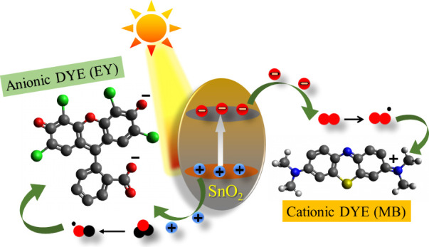
Indeed, the literature reveals the mechanism for dye degradation where it was suggested that when the catalyst surface (SnO2 NPs) is illuminated with light energy higher than its band gap energy, holes (h+) develop in the valence band and electrons (e) reach the conduction band. The electron in the conduction band functions as a reducing agent, reducing the oxygen (O2•) deposited on the surface of the photocatalyst, whereas the holes act as an oxidizing agent, oxidizing the dyes directly or reacting with water to produce hydroxyl radicals (OH•), which further degrade the dyes further. The probable mechanism for the photodegradation of MB and EY dyes using SnO2 photocatalyst can be depicted in Scheme 1.
Scheme 1. Photocatalytic Degradation of MB and EY Using the SnO2 Photocatalyst.
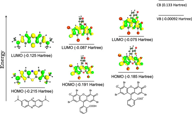
To understand the electronic configuration and spatial orientation of the dyes, a density functional theoretical (DFT) calculation was carried out. The calculation was performed using DFT-D3 (BJ) at the level of B3LYP + COSMO (water) with def2-SVP for every atom using TURBOMOLE Version 7.3 in MAC-OS (see the Supporting Information for the optimized coordinates).64−68 MB and EY crystal structures were considered for the optimization.69,70 Based on the literature, it can be presumed that an electronic transition must be involved from the dye to the material, which eventually degraded the dye. Thus, the primary aim of the calculation was to explore the energy level of different orbitals, especially HOMO and LUMO.
Upon optimization, the HOMO–LUMO gap for MB was observed as −0.09 hartree (Figure 7), whereas for EY, two types of geometry were analyzed considering the overall charge of the molecule as either 1– or 2– charge. Deprotonation of −OH and −COOH was considered for multiple-charge states; double deprotonation would lead to a 2– charge state, whereas for single deprotonation, the overall charge will be 1–. The HOMO–LUMO gap for EY at 1– charge showed −0.104 hartree; at 2– charge, the same was −0.11 hartree. The HOMO–LUMO gap increased for 2– charges, making the electronic transition tougher than that of the single-charged entity. Interestingly, the LUMO of the EY at 2– charge is closer to the valence band of SnO2, thereby making the electron transfer more feasible, whereas considering the MB, the LUMO energy level is lower compared to both charge states of EY. The experimental analysis showed that EY degraded more than 50% within the first hour, whereas MB’s rate was way slower. This can be correlated with the energy levels of dye orbitals and SnO2. Both EY at 1– and 2– showed a closer energy value to the valence band of SnO2; thus, when the holes (h+) act as an oxidizing agent, it can be hypothesized that the electron may transfer from the dye (LUMO) to SnO2 (valence band). Another reason for a lower rate of MB could be the inherent positive charge of MB, which, on the other hand, is negative for EY. Thus, the Coulombic interaction between EY and SnO2 would be higher than MB and SnO2, eventually leading to higher electron transfer.
Figure 7.
HOMO–LUMO electronic distribution of MB and eosin Y, calculated at the levels of B3LYP and def2-SVP with DFT-D3 (BJ).
4. Conclusions
This study presents a method for the retrieval of tin and tin oxide from discarded computer motherboard PCBs, by offering an opportunity for economically viable and sustainable development. Thorough characterization using XRD, SEM, TEM, and XPS confirmed the presence of a pure phase of SnO2 nanoparticles with a size <50 nm. The synthesized SnO2 NPs exhibited excellent photocatalytic degradation of different cationic and anionic dyes such as MB and EY, respectively, under natural sunlight. Moreover, we have shown that the catalyst is capable of degradation (more than 90%) of mixed dyes under similar conditions, considered as an excellent photocatalyst for the photodegradation of other hazardous toxic dyes present in the environment. The reusability of the catalyst nanoparticles was tested for three consecutive cycles and showed good reusability. The idea of using one waste material to remove another waste during wastewater treatment will be greatly impacted by the recovery process for recycling valuable metal from WPCBs. Through interdisciplinary research, this study aims to demonstrate the feasibility and effectiveness of utilizing waste PCBs for the synthesis of SnO2 catalysts for dye degradation. By valorizing e-waste and simultaneously addressing water pollution challenges, this research contributes to the advancement of sustainable technologies for environmental remediation.
Acknowledgments
This work is supported by a Start-up Research Grant. S.S. acknowledges SERB (File No: SRG/2022/001389) for the financial support. S.S. also thanks VIT for providing “VIT SEED GRANT” for carrying out this research work.
Supporting Information Available
The Supporting Information is available free of charge at https://pubs.acs.org/doi/10.1021/acsomega.4c06548.
Elemental mapping of SnO2; EDX analysis; % of dye degradation with an error bar; comparative photocatalytic activities using commercial SnO2; conventional and as-synthesized SnO2; zeta potential of SnO2; photothermal effect on photocatalysis; reusability of the photocatalyst; and post XRD and XPS, and DFT calculation data (PDF)
The authors declare no competing financial interest.
Supplementary Material
References
- Jain M.; Kumar D.; Chaudhary J.; Kumar S.; Sharma S.; Verma A. S. Review on E-waste management and its impact on the environment and society. Waste Manage. Bull. 2023, 1, 34–44. 10.1016/j.wmb.2023.06.004. [DOI] [Google Scholar]
- Liu K.; Tan Q.; Yu J.; Wang M. A global perspective on e-waste recycling. Circular Economy 2023, 2 (1), 100028 10.1016/j.cec.2023.100028. [DOI] [Google Scholar]
- Perkins D. N.; Brune Drisse M.-N.; Nxele T.; Sly P. D. E-waste: a global hazard. Ann. Global Health 2014, 80 (4), 286–295. 10.1016/j.aogh.2014.10.001. [DOI] [PubMed] [Google Scholar]
- Abdelbasir S. M.; El-Sheltawy C. T.; Abdo D. M. Green processes for electronic waste recycling: a review. Journal of Sustainable Metallurgy 2018, 4, 295–311. 10.1007/s40831-018-0175-3. [DOI] [Google Scholar]
- Palanisamy K.; Subburaj R. G. Integration of electronic waste management: a review of current global generation, health impact, and technologies for value recovery and its pertinent management technique. Environmental Science and Pollution Research 2023, 30 (23), 63347–63367. 10.1007/s11356-023-26719-6. [DOI] [PubMed] [Google Scholar]
- Vishwakarma S.; Kumar V.; Arya S.; Tembhare M.; Dutta D.; Kumar S. E-waste in Information and Communication Technology Sector: Existing scenario, management schemes and initiatives. Environ. Technol. Innovation 2022, 27, 102797 10.1016/j.eti.2022.102797. [DOI] [Google Scholar]
- Baldé C. P.; Forti V.; Gray V.; Kuehr R.; Stegmann P.. The global e-waste monitor; United Nations University (UNU), International Telecommunication Union (ITU) & International Solid Waste Association (ISWA): Bonn/Geneva/Vienna, 2017, pp. 1–109. [Google Scholar]
- Liu X.; Liu R.; Lu Y.; Sun Q.; Xue W.; Cheng M.; Yang Y. Efficient and selective gold recovery from e-waste by imidazolium-based poly (ionic liquid) s. Sep. Purif. Technol. 2024, 328, 125049 10.1016/j.seppur.2023.125049. [DOI] [Google Scholar]
- Selvakumar S.; Adithe S.; Isaac J. S.; Pradhan R.; Venkatesh V.; Sampath B.. A Study of the Printed Circuit Board (PCB) E-Waste Recycling Process. In Sustainable Approaches and Strategies for E-Waste Management and Utilization, Rawani A. M., Sahu M. K., Chakarabarti S. S., Singh A. K., Eds.; IGI Global, 2023; pp. 159–184. [Google Scholar]
- Mori de Oliveira C.; Bellopede R.; Tori A.; Marini P. Study of Metal Recovery from Printed Circuit Boards by Physical-Mechanical Treatment Processes. Mater. Proc. 2022, 5 (1), 121. 10.3390/materproc2021005121. [DOI] [Google Scholar]
- Ajekwene K.; Aigbokhan E.; Akindele O.; Yibowei M.; Momoh F.; Ugo U. Electronic Waste (E-Waste): Sources, Proliferation, Effects & Management in Developing Nations. IOSR J. Eng. 2022, 12, 12–27. [Google Scholar]
- Szałatkiewicz J. Metals content in printed circuit board waste. Polym. J. Environ. Stud 2014, 23 (6), 2365–2369. [Google Scholar]
- Killick D.; Fenn T. Archaeometallurgy: the study of preindustrial mining and metallurgy. Annual review of anthropology 2012, 41, 559–575. 10.1146/annurev-anthro-092611-145719. [DOI] [Google Scholar]
- Nagaraj D. R.Minerals recovery and processing. Kirk-Othmer Encycl. Chem. Technol. 2001. DOI: 10.1002/0471238961.1309140514010701.a01. [DOI] [Google Scholar]
- Gautam P.; Behera C. K.; Sinha I.; Gicheva G.; Singh K. K. High added-value materials recovery using electronic scrap-transforming waste to valuable products. Journal of Cleaner Production 2022, 330, 129836 10.1016/j.jclepro.2021.129836. [DOI] [Google Scholar]
- Seif R.; Salem F. Z.; Allam N. K. E-waste recycled materials as efficient catalysts for renewable energy technologies and better environmental sustainability. Environment, Development and Sustainability 2024, 26 (3), 5473–5508. 10.1007/s10668-023-02925-7. [DOI] [PMC free article] [PubMed] [Google Scholar]
- Bhattacharya G.; Fishlock S. J.; McLaughlin J. A.; Roy S. S. Metal-oxide nanomaterials recycled from E-waste and metal industries: A concise review of applications in energy storage, catalysis, and sensing. International Journal of Energy Research 2021, 45 (5), 8091–8102. 10.1002/er.6336. [DOI] [Google Scholar]
- Padha B.; Verma S.; Ahmed A.; Chavhan M. P.; Mahajan P.; Arya S. From trash to treasure: crafting electrochemical supercapacitors with recycled waste materials. Progress in Energy 2024, 6 (1), 012005 10.1088/2516-1083/ad139c. [DOI] [Google Scholar]
- Yang Y.-Y.; Feng H.-P.; Zhang X.-G.; Guo H.; Wen X.-J.; Sui L.; Dong Z.-T.; Yan M.; Niu C.-G. Regulating and protecting of oxygen vacancy endow MoO3-x@Zn2In2S5 S-scheme core–shell heterojunction with high-efficiency organic pollutant removal and bacterial disinfection: Correlation of pollutant active sites to degradation pathways. Chem. Eng. J. 2024, 490, 151309 10.1016/j.cej.2024.151309. [DOI] [Google Scholar]
- Liu H.-Y.; Niu C.-G.; Huang D.-W.; Liang C.; Guo H.; Yang Y.-Y.; Li L. Unravelling the role of reactive oxygen species in ultrathin Z-scheme heterojunction with surface zinc vacancies for photocatalytic H2O2 generation and CTC degradation. Chem. Eng. J. 2023, 465, 143007 10.1016/j.cej.2023.143007. [DOI] [Google Scholar]
- Mallikarjuna K.; Rafiqul Bari G. A. K. M.; Vattikuti S. V. P.; Kim H. Synthesis of carbon-doped SnO2 nanostructures for visible-light-driven photocatalytic hydrogen production from water splitting. Int. J. Hydrogen Energy 2020, 45 (57), 32789–32796. 10.1016/j.ijhydene.2020.02.176. [DOI] [Google Scholar]
- Duverneuil P.; Maury F.; Pebere N.; Senocq F.; Vergnes H. Chemical vapor deposition of SnO2 coatings on Ti plates for the preparation of electrocatalytic anodes. Surf. Coat. Technol. 2002, 151, 9–13. 10.1016/S0257-8972(01)01618-8. [DOI] [Google Scholar]
- Kong Y.; Li Y.; Cui X.; Su L.; Ma D.; Lai T.; Yao L.; Xiao X.; Wang Y. SnO2 nanostructured materials used as gas sensors for the detection of hazardous and flammable gases: A review. Nano Materials Science 2022, 4 (4), 339–350. 10.1016/j.nanoms.2021.05.006. [DOI] [Google Scholar]
- Masuda Y. Recent advances in SnO2 nanostructure based gas sensors. Sens. Actuators, B 2022, 364, 131876 10.1016/j.snb.2022.131876. [DOI] [Google Scholar]
- Dalapati G. K.; Sharma H.; Guchhait A.; Chakrabarty N.; Bamola P.; Liu Q.; Saianand G.; Sai Krishna A. M.; Mukhopadhyay S.; Dey A.; et al. Tin oxide for optoelectronic, photovoltaic and energy storage devices: a review. J.Mater. Chem. A 2021, 9 (31), 16621–16684. 10.1039/D1TA01291F. [DOI] [Google Scholar]
- Pargoletti E.; Hossain U. H.; Di Bernardo I.; Chen H.; Tran-Phu T.; Chiarello G. L.; Lipton-Duffin J.; Pifferi V.; Tricoli A.; Cappelletti G. Engineering of SnO2–graphene oxide nanoheterojunctions for selective room-temperature chemical sensing and optoelectronic devices. ACS Appl. Mater. Interfaces 2020, 12 (35), 39549–39560. 10.1021/acsami.0c09178. [DOI] [PMC free article] [PubMed] [Google Scholar]
- Ma L. A.; Wei Z. H.; Ye X. Y.; Lin J. Y.; Hu L. Q.; Guo T. L. Morphology-controlled synthesis and field-emission properties of patterned SnO2 nanostructures with different morphologies. Ceram. Int. 2017, 43 (8), 6096–6104. 10.1016/j.ceramint.2017.02.002. [DOI] [Google Scholar]
- Pan S.; Gayathri G.; Reshma T. S.; Mangamma G.; Prasad A. K.; Das A. A sensitive humidity sensor at low pressure with SnO2 QDs. Sensors and Actuators A: Physical 2022, 346, 113835 10.1016/j.sna.2022.113835. [DOI] [Google Scholar]
- Wali Q.; Jose R.. Chapter 7 - SnO2 dye-sensitized solar cells. In Nanomaterials for Solar Cell Applications, Thomas S., Sakho E. H. M., Kalarikkal N., Oluwafemi S. O., Wu J., Eds.; Elsevier, 2019; pp. 205–285. [Google Scholar]
- Chen Z.; Yang W.; Chen Y.; Yin X.; Liu Y. Smart coatings embedded with polydopamine-decorated layer-by-layer assembled SnO2 nanocontainers for the corrosion protection of 304 stainless steels. J. Colloid Interface Sci. 2020, 579, 741–753. 10.1016/j.jcis.2020.06.118. [DOI] [PubMed] [Google Scholar]
- Chen M.; Chen X.; Ma W.; Sun X.; Wu L.; Lin X.; Yang Y.; Li R.; Shen D.; Chen Y.; et al. Highly Stable SnO2-Based Quantum-Dot Light-Emitting Diodes with the Conventional Device Structure. ACS Nano 2022, 16 (6), 9631–9639. 10.1021/acsnano.2c02912. [DOI] [PubMed] [Google Scholar]
- Abou- Elyazed A. S.; Hassan S.; Ashry A. G.; Hegazy M. Facile, Efficient, and Cheap Electrode based on SnO2/Activated Carbon Waste for Supercapacitor and Capacitive Deionization Applications. ACS Omega 2022, 7 (23), 19714–19720. 10.1021/acsomega.2c01458. [DOI] [PMC free article] [PubMed] [Google Scholar]
- Patel G. H.; Chaki S. H.; Kannaujiya R. M.; Parekh Z. R.; Hirpara A. B.; Khimani A. J.; Deshpande M. P. Sol-gel synthesis and thermal characterization of SnO2 nanoparticles. Physica B: Condensed Matter 2021, 613, 412987 10.1016/j.physb.2021.412987. [DOI] [Google Scholar]
- Nguyen T. K.; Yu S. H.; Yan J.; Chua D. H. C. SnO2-anchored carbon fibers chemical vapor deposition (CVD) synthesis: effects of growth parameters on morphologies and electrochemical behaviors. J. Mater. Sci. 2020, 55 (32), 15588–15601. 10.1007/s10853-020-05121-4. [DOI] [Google Scholar]
- Divya J.; Pramothkumar A.; Joshua Gnanamuthu S.; Bernice Victoria D. C.; Jobe prabakar P. C. Structural, optical, electrical and magnetic properties of Cu and Ni doped SnO2 nanoparticles prepared via Co-precipitation approach. Physica B: Condensed Matter 2020, 588, 412169 10.1016/j.physb.2020.412169. [DOI] [Google Scholar]
- Zong S.; Zhang Y.; Cao J.; Qin C.; Bala H.; Wang Y. Hydrothermal Synthesis of SnO2 with Different Morphologies as Sensing Materials for HCHO Detection. Langmuir 2024, 40 (20), 10814–10824. 10.1021/acs.langmuir.4c01263. [DOI] [PubMed] [Google Scholar]
- Karmaoui M.; Jorge A. B.; McMillan P. F.; Aliev A. E.; Pullar R. C.; Labrincha J. A.; Tobaldi D. M. One-Step Synthesis, Structure, and Band Gap Properties of SnO2 Nanoparticles Made by a Low Temperature Nonaqueous Sol–Gel Technique. ACS Omega 2018, 3 (10), 13227–13238. 10.1021/acsomega.8b02122. [DOI] [PMC free article] [PubMed] [Google Scholar]
- Jia B.; Jia W.; Wu X.; Qu F. Hierarchical porous SnO2 microflowers photocatalyst. Science of Advanced Materials 2012, 4 (11), 1127–1133. 10.1166/sam.2012.1404. [DOI] [Google Scholar]
- Fatimah I.; Ramanda G. D.; Sagadevan S.; Ghazali S. A. I. S. M.; Ooh W.-C. Ultrasound-assisted phyto-mediated synthesis of SnO2 nanoparticles as photocatalyst in tetracycline photocatalytic oxidation. Inorg. Chem. Commun. 2024, 161, 112096 10.1016/j.inoche.2024.112096. [DOI] [Google Scholar]
- Lellis B.; Fávaro-Polonio C. Z.; Pamphile J. A.; Polonio J. C. Effects of textile dyes on health and the environment and bioremediation potential of living organisms. Biotechnology Research and Innovation 2019, 3 (2), 275–290. 10.1016/j.biori.2019.09.001. [DOI] [Google Scholar]
- Singh A.; Pal D. B.; Mohammad A.; Alhazmi A.; Haque S.; Yoon T.; Srivastava N.; Gupta V. K. Biological remediation technologies for dyes and heavy metals in wastewater treatment: New insight. Bioresour. Technol. 2022, 343, 126154 10.1016/j.biortech.2021.126154. [DOI] [PubMed] [Google Scholar]
- Mahmood A.; Bilal B.; Naeem Z.; Iram S. Physical, chemical, and biological remediation techniques for textile effluents in context with developed and developing countries. Rhizobiont in bioremediation of hazardous waste 2021, 409–441. 10.1007/978-981-16-0602-1_18. [DOI] [Google Scholar]
- Rajeshwar K.; Osugi M.; Chanmanee W.; Chenthamarakshan C.; Zanoni M. V. B.; Kajitvichyanukul P.; Krishnan-Ayer R. Heterogeneous photocatalytic treatment of organic dyes in air and aqueous media. J. Photoch. Photobio. C: photochemistry reviews 2008, 9 (4), 171–192. 10.1016/j.jphotochemrev.2008.09.001. [DOI] [Google Scholar]
- Nascimento M. A.; Castro Cruz J.; dos Reis M. F.; de Carvalho Damasceno O. I.; Lázaro Reis E.; Reis C.; de Oliveira A. F.; Pereira Lopes R. Synthesis of polymetallic nanoparticles from printed circuit board waste and application in textile dye remediation. J. Environ. Chem. Eng. 2018, 6 (4), 5580–5586. 10.1016/j.jece.2018.08.056. [DOI] [Google Scholar]
- Khayyam Nekouei R.; Pahlevani F.; Mayyas M.; Maroufi S.; Sahajwalla V. Direct transformation of waste printed circuit boards into high surface area t-SnO2 for photocatalytic dye degradation. J. Environ. Chem. Eng. 2019, 7, 103133 10.1016/j.jece.2019.103133. [DOI] [Google Scholar]
- Yoo K.; Lee K.; Jha M. K.; Lee J.-C.; Cho K. Preparation of nano-sized tin oxide powder from waste Pb-free solder by direct nitric acid leaching. J. Nanosci. Nanotechnol. 2016, 16 (11), 11238–11241. 10.1166/jnn.2016.13485. [DOI] [Google Scholar]
- Mecucci A.; Scott K. Leaching and electrochemical recovery of copper, lead and tin from scrap printed circuit boards. J. Chem.Technol. Biotechnol. 2002, 77 (4), 449–457. 10.1002/jctb.575. [DOI] [Google Scholar]
- Solar radiation in Chennai https://en.tutiempo.net/solar-radiation/chennai.html.
- Sagadevan S.; Lett J. A.; Alshahateet S. F.; Fatimah I.; Weldegebrieal G. K.; Le M.-V.; Leonard E.; Paiman S.; Soga T. Photocatalytic degradation of methylene blue dye under direct sunlight irradiation using SnO2 nanoparticles. Inorg. Chem. Commun. 2022, 141, 109547 10.1016/j.inoche.2022.109547. [DOI] [Google Scholar]
- Sen S. K.; Hossain M. S.; Roy R.; Alam M. S.; Manir M. S.; Biswas G. G. Size-strain distribution analysis from XRD peak profile of (Mg, Fe) co-doped SnO2 nanoparticles fabricated using chemical co-precipitation route. Ceram. Int. 2024, 50 (21), 44038–44055. 10.1016/j.ceramint.2024.08.254. [DOI] [Google Scholar]
- Deepa S.; Philip A. M.; George A. S.; Prasannakumari K. Microstructural, optical and dielectric variations in SnO2 nanoparticles synthesized via surfactant-assisted sol–gel route. Bull. Mater. Sci. 2021, 44 (4), 283. 10.1007/s12034-021-02567-3. [DOI] [Google Scholar]
- Gesesse G. D.; Gomis-Berenguer A.; Barthe M.-F.; Ania C. O. On the analysis of diffuse reflectance measurements to estimate the optical properties of amorphous porous carbons and semiconductor/carbon catalysts. J. Photochem. Photobiol., A 2020, 398, 112622 10.1016/j.jphotochem.2020.112622. [DOI] [Google Scholar]
- Abdullahi S. S.; Güner S.; Musa Y.; Adamu B. I.; Abdulhamid M. I. Simple method for the determinatıon of band gap of a nanopowdered sample usıng Kubelka Munk theory. NAMP J. 2016, 35, 241–246. [Google Scholar]
- Bonu V.; Das A.; Sardar M.; Dhara S.; Tyagi A. K. Surface functionalization-enhanced magnetism in SnO2 nanoparticles and its correlation to photoluminescence properties. J. Mater. Chem. C 2015, 3 (6), 1261–1267. 10.1039/C4TC02210F. [DOI] [Google Scholar]
- Dieguez A.; Romano-Rodrıguez A.; Vila A.; Morante J. The complete Raman spectrum of nanometric SnO2 particles. J. Appl. Phys. 2001, 90 (3), 1550–1557. 10.1063/1.1385573. [DOI] [Google Scholar]
- Leonardy A.; Hung W.-Z.; Tsai D.-S.; Chou C.-C.; Huang Y.-S. Structural features of SnO2 nanowires and raman spectroscopy analysis. Cryst. Growth Des. 2009, 9 (9), 3958–3963. 10.1021/cg9000957. [DOI] [Google Scholar]
- Peercy P.; Morosin B. Pressure and temperature dependences of the Raman-active phonons in Sn O2. Phys. Rev. B 1973, 7 (6), 2779. 10.1103/PhysRevB.7.2779. [DOI] [Google Scholar]
- Houas A.; Lachheb H.; Ksibi M.; Elaloui E.; Guillard C.; Herrmann J.-M. Photocatalytic degradation pathway of methylene blue in water. Appl. Catal. B: Environmental 2001, 31 (2), 145–157. 10.1016/S0926-3373(00)00276-9. [DOI] [Google Scholar]
- Fan Q.-Q.; Niu C.-G.; Guo H.; Huang D.-W.; Dong Z.-T.; Yang Y.-Y.; Liu H.-Y.; Li L.; Qin M.-Z. Insights into the role of reactive oxygen species in photocatalytic H2O2 generation and OTC removal over a novel BN/Zn3In2S6 heterojunction. J. Hazard. Mater. 2022, 438, 129483 10.1016/j.jhazmat.2022.129483. [DOI] [PubMed] [Google Scholar]
- Zhang X.; Yang P.; Chen H. S.; Jiang S. P. Carbon layer derived carrier transport in Co/g-C3N4 nanosheet junctions for efficient H2O2 production and NO removal. Chem. Eng. J. 2024, 479, 147609 10.1016/j.cej.2023.147609. [DOI] [Google Scholar]
- Kalaycıoğlu Z.; Özuğur Uysal B.; Pekcan Ö.; Erim F. B. Efficient Photocatalytic Degradation of Methylene Blue Dye from Aqueous Solution with Cerium Oxide Nanoparticles and Graphene Oxide-Doped Polyacrylamide. ACS Omega 2023, 8 (14), 13004–13015. 10.1021/acsomega.3c00198. [DOI] [PMC free article] [PubMed] [Google Scholar]
- Sagadevan S.; Anita Lett J.; Alshahateet S. F.; Fatimah I.; Weldegebrieal G. K.; Le M.-V.; Leonard E.; Paiman S.; Soga T. Photocatalytic degradation of methylene blue dye under direct sunlight irradiation using SnO2 nanoparticles. Inorg. Chem. Commun. 2022, 141, 109547 10.1016/j.inoche.2022.109547. [DOI] [Google Scholar]
- Chiu H.-C.; Yeh C.-S. Hydrothermal Synthesis of SnO2 Nanoparticles and Their Gas-Sensing of Alcohol. J. Phys. Chem. C 2007, 111 (20), 7256–7259. 10.1021/jp0688355. [DOI] [Google Scholar]
- TURBOMOLE V.7.3, a development of University of Karlsruhe and Forschungszentrum Karlsruhe GmbH, 1989–2007. In TURBOMOLE GmbH, 2007. [Google Scholar]
- Ghosh P.; Maayan G. A Water-Soluble Peptoid that Can Extract Cu2+ from Metallothionein via Selective Recognition. Chem. - Eur. J. 2021, 27 (4), 1383–1389. 10.1002/chem.202003711. [DOI] [PubMed] [Google Scholar]
- Halder S.; Barma A.; Rizzoli C.; Ghosh P.; Roy P. Density Functional Theory Analysis of Host–Guest Interactions in Cu(II)-Based Metal–Organic Frameworks for Pesticide Detection. ACS Appl. Nano Mater. 2019, 2, 5469–5474. 10.1021/acsanm.9b01067. [DOI] [Google Scholar]
- Ghosh P.; Ruan G.; Fridman N.; Maayan G. Amide bond hydrolysis of peptoids. Chem. Commun. 2022, 58 (71), 9922–9925. 10.1039/D2CC02717H. [DOI] [PubMed] [Google Scholar]
- Ghosh P.; Maayan G. A rationally designed peptoid for the selective chelation of Zn2+ over Cu2+. Chem. Sci. 2020, 11 (37), 10127–10134. 10.1039/D0SC03391J. [DOI] [PMC free article] [PubMed] [Google Scholar]
- Caldeweyher E.; Bannwarth C.; Grimme S. Extension of the D3 dispersion coefficient model. J. Chem. Phys. 2017, 147 (3), 034112 10.1063/1.4993215. [DOI] [PubMed] [Google Scholar]
- Quint V.; Morlet-Savary F.; Lohier J.-F.; Lalevee J.; Gaumont A.-C.; Lakhdar S. Metal-free, visible light-photocatalyzed synthesis of benzo [b] phosphole oxides: synthetic and mechanistic investigations. J. Am. Chem. Soc. 2016, 138 (23), 7436–7441. 10.1021/jacs.6b04069. [DOI] [PubMed] [Google Scholar]
Associated Data
This section collects any data citations, data availability statements, or supplementary materials included in this article.


