Abstract
Monocrystalline graphene growth has always been an intriguing research focus. Argon (Ar) is merely viewed as a carrier gas due to its inert chemical properties throughout the whole growth procedure by the chemical vapor deposition method. In this work, the influence of Ar on temperature and flow fields was investigated in consideration of its physical parameter difference among all involved gases. Results by experimental characterization and fluid dynamics simulation showed that the temperature elevated, and the velocity of the mixed gas increased as the Ar flow rates rose. Furthermore, the deposition rate of C on the Cu surface, representing graphene generation rate, was studied as the Ar flow rate changed in combination with CH4 decomposition reaction. Based on the effects made by Ar, a method was proposed, where the Ar flow rate was dynamically regulated to break monocrystalline graphene growth cessation. The graphene size was enlarged, and the nucleation site density was reduced remarkably compared with a common consistent Ar flow. It is believed that this work would provide a new perspective in two-dimensional material preparation by combining basic properties with temperature and field distribution in the whole reaction system.
Introduction
Graphene, as a two-dimensional material with excellent electrical, thermal, and mechanical properties, has demonstrated a wide range of applications in the fields of energy, electronics, optics, and biomedicine.1−9 The prerequisite for realizing these applications was to grow high-quality graphene with tunable sizes. Since the single graphene sheet was first isolated, research studies on various graphene-based applications have been studied extensively.10−12 The successful preparation of semiconductor graphene provides the possibility for the transition of the integrated circuit field from traditional silicon-based devices to carbon-based devices.13 Although the mechanical exfoliated graphene has a high quality,14 its industrial application is limited by the micrometer size. Numerous methods have been employed for synthesizing large-size graphene.15−17 Among them, chemical vapor deposition (CVD) based on a metal substrate has become the most favored method to prepare graphene materials due to its convenience and cost-friendliness.18−24 Based on the low carbon solubility, the growth of graphene on Cu substrates follows the surface adsorption mechanism, and large-area uniform monolayer graphene films were successfully synthesized by Ruoff’s group in 2009.18,25 Nevertheless, the growth of graphene on metallic Cu substrates is a typical self-reconfiguration process of uncorrelated nucleation sites, and the properties of graphene are severely weakened by the presence of grain boundaries.26−28 Controlling the formation of grain boundaries and synthesizing high-quality monocrystalline graphene are regarded to be important tasks in the graphene preparation process.
At present, large-size monocrystalline graphene obtained by stitching multiple graphene domains with uniform orientation on the Cu substrate has been developed by researchers.18,29−32 However, the complexity of Cu substrate preparation and the tiny mismatch for this method restricted its application in industrial production. In addition, sustained growth of individual graphene domains by eliminating the density of nucleation sites is another strategy for obtaining high-quality monocrystalline graphene.33−37 The key to this strategy lies in passivating the density of graphene on the Cu substrate and enhancing the graphene growth rate. In recent years, the nucleation density of graphene was decreased by controlling growth parameters, including temperature, pressure, gas flow rate, substrate, and so on.38−44 Herein, the gas flow plays a crucial role in regulating substance transport and surface chemistry during the CVD process. A large number of studies have focused on the significance of the carbon source gas CH4 and the reaction gas H2 for the growth of single-crystal graphene. Li’s team demonstrated that the nucleation density of graphene decreases with CH4 flow rate, which is incompatible with generating the lateral growth rates necessary for rapid graphene growth.45 Eres et al. described the balance between the nucleation density and the lateral graphene growth rate, and 0.5 sccm CH4 was considered as an optimum balance inflection point for graphene growth.46 Wu et al. employed a CH4 gradient supply method, initially introducing lower CH4 fluxes to form fewer nucleation sites at the beginning of growth and gradually increasing CH4 fluxes over time to provide abundant carbon source and enhance graphene growth rates.35 In addition, the role of H2 in CVD growth of single-crystal graphene has been investigated and a dual role of H2 as an activator of the surface-bound carbon and an etching reagent that controls the size of graphene domains were revealed.47,48 Referring to Ar, the quantity of Ar flow directly has an impact on regulating CH4 partial pressure. Except this, it is merely viewed as a carrier gas because of its inert chemical quality. Hence, the Ar flow is maintained at a specific value throughout the growth process, and few studies concerned its effect on graphene synthesis.
In this paper, based on the basic physical properties and diversity of gases participating in the reaction, the temperature and material fields at different Ar flow rates are investigated by experiments and computational fluid dynamics (CFD) simulation. Under the guidance of the numerical computation, an Ar regulation method (ARM) was designed to offer a growth driving force for graphene synthesis.
Materials and Methods
Graphene Synthesis
To flatten the substrate surface, a commercial Cu foil (50 μm, 99.9%, ZHAOHUI copper) was placed in the phosphoric acid electrolyte and electrochemically polished using an electrochemical polishing station with a voltage of 1.8 V for 30 min. The Cu foil was rinsed with deionized water and ethanol and dried with an Ar flow. The preprocessed Cu foil was placed in a quartz boat to maintain quasi-static equilibrium, which was pushed in the heating zone of the quartz tube in the furnace, and then the tube was vacuumed by a mechanical pump. 500 sccm Ar was introduced, and the pressure was controlled at 0.5 atm in the chamber by a vacuum valve. The tube was heated to 1050 °C at a ramp rate of 10 °C/min, and 10 sccm H2 was injected to anneal the Cu substrate for 60 min. During the graphene growth, methane gas (0.1% in Ar) at 30 sccm was flown as the carbon source. As the Ar flow changed, the vacuum valve was adjusted to maintain a constant pressure in the furnace. After graphene growth, the CH4 supply was cut off, and the furnace chamber was exposed to air for cooling to room temperature rapidly while under the same Ar and H2 flow.
Graphene Transfer
The grown graphene on Cu foil was transferred to the target substrate (e.g., SiO2/Si, Cu grid) by the poly(methyl methacrylate) (PMMA)-assisted wet method. First, PMMA was uniformly coated on the surface of the graphene/Cu samples at 3000 rpm. Second, the samples were heated for 5 min at 120 °C, and then, the PMMA/graphene/Cu structure was placed on the surface of the etching solution (10 wt % FeCl3) for 2 h. After etching, the sample was cleaned three times with deionized water. Next, the floating PMMA/graphene layer was scooped using the target substrate and dried in air for 12 h. Finally, the PMMA layer was dissolved away by acetone solution to expose the graphene surface.
Characterization of Graphene
The morphological images of graphene on Cu foil and SiO2/Si substrate were taken by an optical microscope (OM, OLYMPUS BX53M). Raman spectra and maps of graphene were obtained using a Raman system (LabRAM HR spectrometer, HORIBA) with a 532 nm excitation laser to analyze the quality and uniformity of the graphene layers. The graphene on 200 mesh Cu grids was characterized by transmission electron microscopy (TEM, JEM-2100F). Atomic force microscopy (AFM, Dimension Icon, Bruker) was used to measure the mechanical strength of graphene in the peak force tapping mode.
CFD Numerical Simulation
Commercial software ANSYS Fluent was used to perform CVD simulations. The CVD geometric model was developed by SolidWorks, where the reaction surface with material properties defined as Cu was created to simulate the graphene deposition process. The geometric model contains 1.8 million grid cells, which were generated by Fluent Meshing. Laminar flow was applied as the physical model, and the numerical calculations based on energy, component transport, and chemical surface reaction equations were employed to investigate temperature field, flow field, and concentration field in a tube furnace. Pressure Implicit with Splitting of Operators (PISO) solver was set, which significantly improved convergence speed. After calculation, CFD-post was used for postprocessing.
Results and Discussion
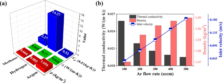
The basic physical properties of Ar, H2, and CH4 including gas density (ρ), thermal conductivity (λ), and specific heat capacity at constant pressure (Cp) are shown in Figure 1a. Under standard conditions, the gas density of H2 (0.083 kg/m3) is only one-twentieth that of Ar (1.654 kg/m3). It means that the small mass of H2 molecules owned faster diffusion rate compared to Ar molecules in a horizontal furnace. λ and Cp are most important thermal properties and play a key role in the temperature distribution during graphene growth. The Cp values of the gas were represented by the blue chart, which showed that the H2 [14.27 kJ/(kg K)] ranks the highest, Ar [0.52 kJ/(kg K)] owns the lowest, and CH4 [2.27 kJ/(kg K)] is in the middle. In addition, the λ of Ar [0.018 W/(m K)] was almost one-tenth of that of H2 [0.17 W/(m K)]. From the comparison of value, it can be elucidated that under same growth temperature, changing the reaction gases ratio would make great effect on both temperature and fluid field distribution. The influence of the Ar gas flow rate variation on the physical parameters of the mixed gas was investigated and is shown in Figure 1b. For thermal properties, thermal conductivity λ is mainly discussed as thermal conductivity λ is in proportion to Cp according to the equation λ = α•ρ•Cp. The thermal conductivity λ of the mixed gas is negatively correlated with the Ar flow rate which decreased from 0.026 to 0.020 W/(m K) as the Ar flow rate ranges from 100 to 500 sccm. On the contrary, the density of mixed gas displayed a positive relation to Ar flow rate. Therefore, lower Ar flow rate is supposed to possess higher heat transfer and faster diffusion rates. The inlet velocity of the mixed gas was calculated and is shown by the blue line in Figure 1b, and the lower flow rate allows the carbon source to remain on the substrate surface for a longer period of time. Based on the above results, it is believed that the Ar flow rate variation will simultaneously affect the temperature distribution of the furnace besides the common sense as a carrier gas for carbon source.
Figure 1.
(a) Basic physical parameter comparison of three gases used for CVD graphene synthesis under standard conditions. The red, green, and blue bars correspond to the density, thermal conductivity, and constant pressure specific heat capacity of the gas, respectively. (b) Physical parameters of the mixed gas and inlet flow velocity of the furnace chamber at different Ar flow rates.
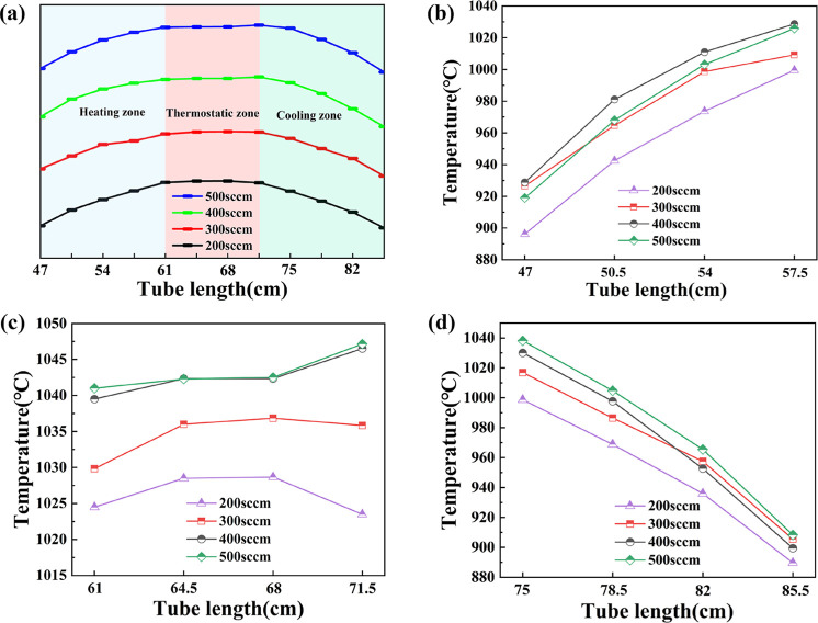
Figure 2a shows the temperature field distribution in the whole furnace at different Ar flow rates through experimental measurement. Except for the Ar flow, the rest of all parameters were kept the same: the furnace temperature was set at 1050 °C, which was the commonly used graphene growth temperature; the pressure was set at 1 atm, and H2 flow was maintained at 10 sccm.
Figure 2.
(a) Temperature field distributions corresponding to four different Ar flow rates. (b–d) Temperature values of different furnace zones under four typical Ar flow rates measured in experiments.
The same temperature distribution at four different Ar flow rates exhibited the same trend in Figure 2a, which corresponded to the heating zone, thermostatic zone, and cooling zone of the tube furnace, respectively. In the two-heater furnace we used in this paper, the length of the thermostatic zone was about 10 cm. As the Ar flow rates increased from 200 to 500 sccm, the measured temperature went up with the maximum temperature raising from 1027 to 1047 °C. The heating and cooling zones away from the center of the heater displayed almost identical trend, as shown in Figure 2b and d. The experimental measurement proved that the change in Ar flow rate indeed impacted the temperature field directly. Lower Ar flow rate was accompanied by lower temperature as higher thermal conductivity λ takes away the heat quickly within the furnace.
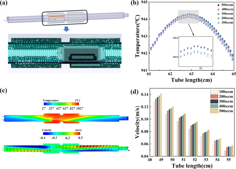
A three-dimensional CFD model with chemical reactions was performed to evaluate the temperature and flow field distribution as shown in Figure 3. The size and assembling of simulation models were constructed strictly based on the tube furnace CVD system and quartz boat for domain-limited reactions. As shown in Figure 3a, fluent meshing was used to mesh the model, and the grids around the quartz boat were encrypted to improve the computational accuracy. The temperature and velocity contour around the furnace model when the Ar flow rate was 500 sccm are displayed in Figure 3c. Given the feature difference and gravity influence on the gas flow, an uneven temperature distribution within the furnace was observed. The profile of the quartz boat reactor was represented by the white line in the contour. The temperatures of different Ar flow rate conditions within the furnace were simulated. Temperature values inside the square quartz boat at different Ar flow rates were extracted and are shown in Figure 3b, and the inset shows enlarged view of the selected area, which corresponds to the Cu foil location area. Apparently, as the Ar flow rates decreased, the maximum temperature values within the quartz boat became lower, which was in good agreement with that experimentally observed. Figure 3c displays the temperature and corresponding gas flow contour, where the magnitude and direction of the gas flow were represented by the black arrows. The gas flow distribution showed a faster gas flow rate near the wall of the furnace chamber, which decreased as the gas flow passed in front of the quartz boat. As shown in Figure 3c, the gas flow rate in the quartz boat reactor was extremely low, and the graphene growth proceeded under the condition of suppressing local reactants nearby the Cu surface.49 Gas velocity distribution before quartz boat at different Ar flow rates is displayed in Figure 3d. Apparently, the gas velocity was proportional to the Ar flow rate at a given position. The gas velocity ascended approximately 0.01 m/s as the flow increased from 100 to 500 sccm. Because of the confinement effect made by the quartz boat reactor, the gas velocities at different Ar flow rates were gradually reduced as getting closer to it. Taking the gas flow of 500 sccm for example, gas velocity declined from 0.14 to 0.06 m/s.
Figure 3.
(a) Schematic of the quartz tube model used for graphene growth and details of the meshing of the heating zone. (b) Simulation results of temperature field inside the quartz boat at different argon flow rates. (c) Contour maps of temperature and velocity distribution with 500 sccm Ar flow rate; the direction of gas flow in the furnace chamber was indicated by a black arrow. Carbon deposition rates on the reaction surface. (d) Velocity comparison before the quartz boat at different Ar flow rates.
In order to further combine simulation to actual graphene growth by the CVD method, two mechanistic processes were performed during the fluid simulations: component transport and reactive deposition of CH4 on the surface, respectively. Gas species reached the reactor surface over the boundary layer, where hydrocarbon precursors decomposed to C species at the reaction surface and then formed a graphene film. The effect of variations in Ar flow rate on the surface deposition rate was investigated, and only the total reaction process of CH4 depositing carbon on the reaction surface was considered. The surface chemical reaction equation during the simulation can be described as
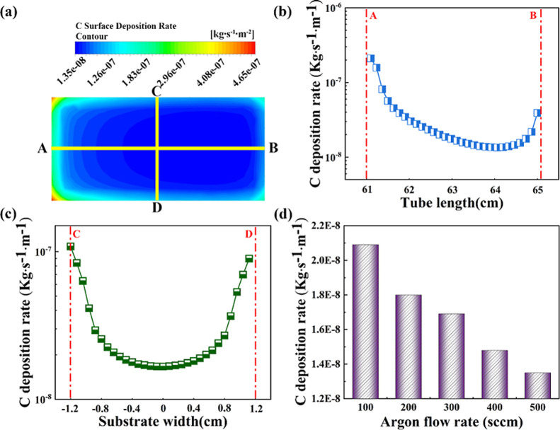
where Cu represent the catalytic effect of the metal substrate on the decomposition of CH4 and Ks is a chemical reaction rate constant whose value is related to the temperature of the reaction surface and the activation energy of the reaction. Figure 4a shows the simulation results of the C surface deposition rate on Cu location area when the Ar flow rate was 500 sccm, where the deposition rate was faster at the boundary of the reaction surface, with a maximum of 4.65 × 10⁻⁷ kg s–1 m–2, and the deposition rate in the middle region of the reaction surface dropped by an order of magnitude to 1.35 × 10⁻⁸ kg s–1 m–2. The distribution of C deposition rates along the horizontal and vertical yellow lines is shown in Figure 4b and c. The highest value emerged at position A, which was closer to the gas inlet. Figure 4c shows a virtually symmetrical distribution of C deposition rates in the vertical direction of the reaction surface. The minimum value of the C deposition rate is indicated by blue color in Figure 4a, and the value was employed to analyze the difference at various Ar flow rates. Figure 4d shows that the C deposition rate increased with decreasing Ar flow rate. Compared to 500 sccm Ar (1.3 × 10⁻⁸ kg s–1 m–2), the C deposition rate increased 1.5 times at 100 sccm Ar (2.1 × 10⁻⁸ kg s–1 m–2), which was attributed to the comprehensive effect of higher CH4 partial pressure, lower temperature, and flow velocity at a low Ar flow rate.
Figure 4.
(a) Contour maps of C deposition rates on the reaction surface. (b,c) Distribution of C deposition rates along the horizontal and vertical lines in (a). (d) Variation tendency of carbon deposition rate at different argon flow rates on the reaction surface.
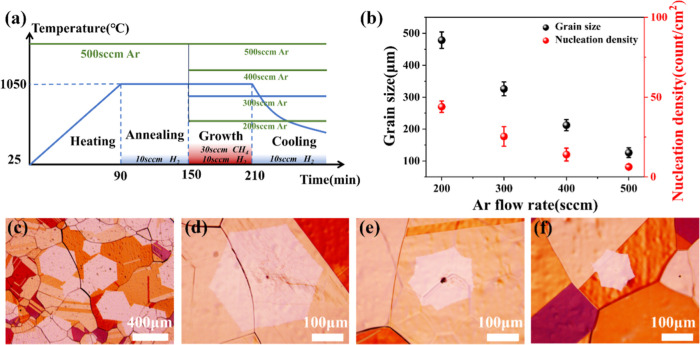
Based on the above theoretical guidance, the growth habit of graphene under a stable Ar gas flow was first investigated. The most conventional hot-wall CVD equipment was employed to improve the applicability of graphene preparation. Figure 5a shows a schematic of the temperature and gas flow during graphene growth over time. CH4 and H2 gas were kept constant at the growth phase, while four different Ar fluxes (200, 300, 400, and 500 sccm) were injected into the quartz tube, and chamber pressure was maintained at 0.5 atm by adjusting the vacuum valve. To visualize the graphene domains, the samples were oxidized in air on a hot plate at 200 °C for 2 min. Figure 5c–f shows the results of graphene grown on Cu with the Ar flow increased from 200 to 500 sccm, and the lower magnification OM images from various locations are shown in Figure S1. It is obvious that the graphene dimension had a great difference after growth for 60 min. The graphene sizes at four different Ar flow rates were 450, 320, 200, and 120 μm, respectively. As shown in Figure 4d, when the Ar flow rate was 500 sccm, numerical simulations displayed the lowest C deposition rate (1.3 × 10⁻⁸ kg s–1 m–2) on the substrate with higher temperature (1042 °C). Conversely, the C deposition rate elevated (2.1 × 10⁻⁸ kg s–1 m–2) when the Ar flow rate was reduced to 200 sccm, which was consistent with the results observed in the experiments. During graphene growth, carbon precursor concentration played a key role in the nucleation and growth rate of graphene, which is usually affected by the Ar flow rates. As shown in Figure 5b, although the grain size of graphene increased when the flow of Ar decreased from 500 to 200 sccm, higher graphene nucleation sites (∼48/cm2) and coverages make adjacent graphene grains interconnected, which is detrimental to the diameter expansion growth of individual graphene domains. Both graphene size and nucleation density were inversely proportional to Ar flow rates, as shown in Figure 5b. This result was attributed to the diluting effect of Ar on CH4, the gas flow rate with high Ar flux was faster, and the CH4 concentration was lower, and few C species were adsorbed on the surface of Cu substrates for nucleation and growth, insulating a low nucleation density and growth rate of graphene. A decrease in Ar flow showed the opposite results; lower Ar flow generated a higher nucleation density and a larger grain size. Based on the above results, it can be seen that under a stable Ar gas flow, the graphene growth will reach equilibrium and terminated to expand in size dimension as it was situated in a fixed temperature and flow field distribution. Consequently, the stable conditions were not the optimal conditions for expansion growth of monocrystalline domain graphene.
Figure 5.
(a) Schematic diagram of the graphene growth process including temperature and gas flow over time. (b) Graphene nucleation density and grain size under four different Ar flow rates (three reduplicate experimental results contained under each Ar flow rate condition). (c–f) OM images of graphene domains grown on Cu substrates corresponding to Ar fluxes of 200, 300, 400, and 500 sccm, respectively.
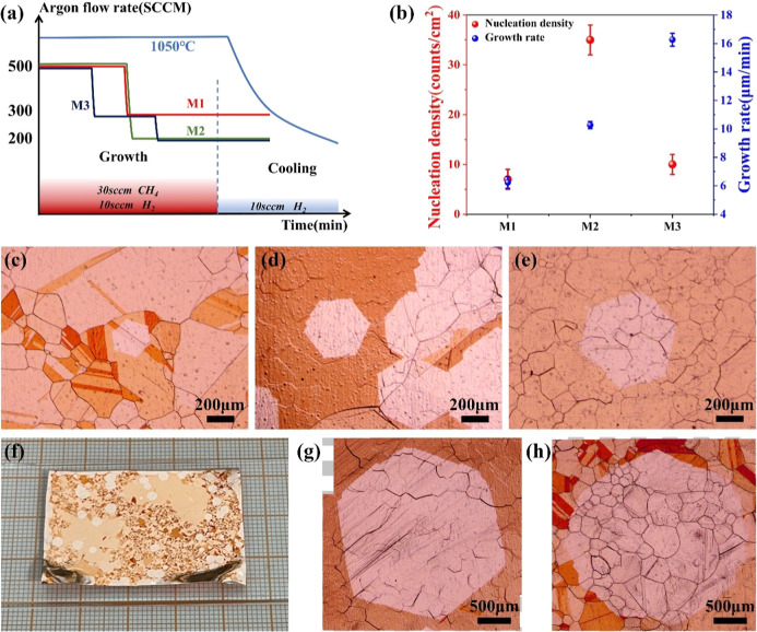
Aiming at providing growth drive force and simultaneously reducing graphene nucleation density, a strategy (Ar-regulation method, ARM) was developed by dynamically modulating Ar flow rate variations during the growth stage. As shown in Figure 6a, three different Ar flow regulation methods were adjusted from high to low Ar flow rate in view of low nucleation density in 500 sccm Ar flow. After growth for 30 min, two of these procedures were performed with argon flow directly reduced from 500 to 300 sccm (M1) and 200 sccm (M2), respectively. And the remaining method is a gradient descent of the Ar flow from 500 to 300 sccm and then 200 sccm (M3). Figure 6c–e shows the optical images of Cu-based graphene prepared by three regulation methods. Except for the dynamic adjustment of the Ar flow rate, the other growth conditions of graphene were kept consistent with the steady flux. The sample sizes obtained from three different regulation methods were 380, 600, and 950 μm, respectively. The corresponding nucleation densities and growth rates are shown in Figure 6b. The highest nucleation density (∼35/cm2) was observed in M2, corresponding to a growth rate that was at a medium level, which differed from growth results under stable Ar flow rates. A possible explanation for this might be that when the Ar flux was reduced to 200 sccm, the concentration of C species within the gas stream increased dramatically, and the nucleation rate of graphene was accelerated by greater supersaturation, which inhibited the diameter expansion of an individual crystalline domain. Despite the lowest nucleation density of the M1 approach, the graphene growth rate was only ∼6 μm/min. OM images at different locations showed same phenomenon on the whole sample, as shown in Figure S2. Compared to the rest of the methods, M3 simultaneously achieved low nucleation density (∼10/cm2) and high growth rate (∼16 μm/min). A digital photograph of the graphene sample grown on a Cu substrate is shown in Figure 6f. When the growth time was extended, large single-crystal graphene domains with a diameter of 3.2 mm were prepared using the M3 method, as shown in Figures 6g,h. The SEM result of the millimeter size domain of graphene and an enlarged detailed image are further characterized in Figure S3.
Figure 6.
(a) Schematic diagram of different dynamic regulation methods of Ar flow rate. (b) Graphene nucleation density and growth rate under three different methods (three reduplicate experimental results contained under each method). (c–e) OM images of the grown graphene by the method of M1, M2, and M3, respectively. (f) Digital image of graphene grown on the Cu substrate by the M3 method. (g,h) OM images of the monocrystalline graphene with a diameter of ∼3 mm.
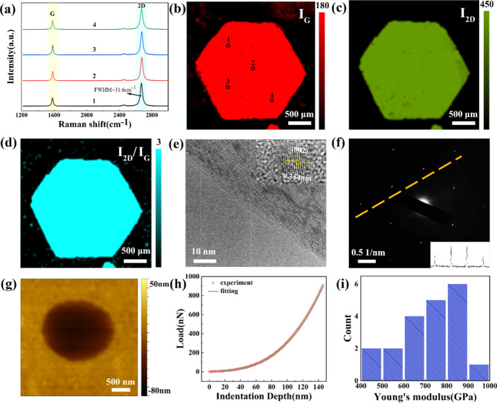
Raman spectroscopy, HRTEM, and AFM were employed to determine the quality of the graphene crystal domains. The samples transferred on the SiO2/Si substrate were subjected to Raman analysis. Figure 7a shows the four Raman spectra extracted from four regions in the mapped area. The Raman shifts of the G and 2D bands were 1583 and 2680 cm–1, respectively, which are two typical Raman features of graphene. The full width at half-maxima of the 2D band was 31.6 cm–1, indicating the monolayer property of the prepared graphene.50 The D peak at 1350 cm–1 was absent, which proves that the graphene possesses a high quality. Raman intensity mapping of the G band (IG), 2D band (I2D), and I2D/IG is shown in Figures 7b–d. The red area in Figure 7b exhibits the typical hexagonal structure of monocrystalline graphene domain. In particular, the uniform Raman signal in the Raman mapping on the graphene sample suggested their uniform qualities. The high I2D/IG ratio (>2) in Figure 7d indicated that the graphene is a monolayer. The morphology of graphene was further observed by HRTEM. Figure 7e shows the edge morphology of graphene after transferring to the Cu gird, the edge shown as a straight line, indicating that the transferred graphene was mainly a single layer. The inset clearly showed the graphene lattice stripes with a crystallographic direction of (002), and the lattice spacing was 0.354 nm, which exhibited a typical characteristic of graphene. The SAED pattern shown in Figure 7f displays a hexagonal diffraction, and the diffraction spot intensity distribution along the orange dotted line is shown in the inset of Figure 7f. The result showed that the diffraction spot intensity ratio (inner to outer) was approximately 2, which further confirmed the monolayer of graphene. The AFM nanoindentation was employed to measure the mechanical properties of graphene. Graphene suspended on the circular hole with a diameter of 2 μm was loaded by the probe tip, and the load—displacement curve was obtained to calculate the Young’s modulus of graphene. After being loaded by a force of 2 μN, the height difference between the graphene film at the center of the hole and the substrate was about 60 nm (Figure 7g). A representative load—displacement curve of the graphene is shown in Figure 7h, which has been well fitted by the quasi-empirical polynomial form.51 The experimental and fitted data were displayed by red boxes and a green solid line, respectively, as shown in Figure 7h. The cubic term fitting parameter yields an elastic modulus E2D of 275 N/m, with a theoretical graphene thickness of 0.335 nm, and the 3D Young’s modulus of graphene was calculated to be 821 GPa, near that of the intrinsic graphene(∼1TPa). Measurement data of 20 freestanding graphene samples were recorded in order to obtain statistical data on elastic stiffness. Figure 7i shows a histogram of mechanical strength, and the Young’s modulus data focused on 700–900 GPa demonstrated the uniformity of the high mechanical strength of monocrystalline graphene.
Figure 7.
(a) Raman spectral data obtained from randomly selected points of the graphene domain in (b). (b–d) Raman mappings of millimeter-scale graphene synthesized by ARM: (b) IG, (c) I2D, and (d) I2D/IG. (e) HRTEM image of the edge morphology of graphene transferred to the Cu gird. The inset clearly shows the graphene lattice stripes with the crystallographic direction of (002). (f) SAED patterns of random location in the graphene sample; the inset shows the diffraction spot intensity distribution along the dotted line. (g) AFM image of free-standing monolayer graphene after loading with 2 μN force. (h) Typical curve of force measured with 900 nN force on grown graphene. (i) Histogram of Young’s modulus of the graphene sample.
In order to elaborate the mechanism of graphene synthesized underneath ARM, boundary layer δ and surface chemical reaction rates K based on the temperature and fluid field distributions were calculated. The boundary layer was formed by the velocity gradient of gas between the bulk gas stream and the surface near the substrate. The thickness of δ is affected by the fluid Reynolds number (Re), which can be expressed by the equation52
where d is the characteristic length of the flow field, ν is the fluid velocity, and ρ and μ are fluid density and dynamic viscosity, respectively. The average thickness of δ over a substrate of length L is related to the Re by equation52
The values of Re and δ at different Ar flow rates listed in Table 1 showed that the thickness of δ became thicker as the Ar flow rate decreased.
Table 1. Values of Re, δ, K, and C Deposition Rate under Different Ar Flow Rates.
| 500 sccm | 300 sccm | 200 sccm | |
|---|---|---|---|
| V (m/s) | 0.014 | 0.013 | 0.012 |
| Re | 19.31 | 17.77 | 16.23 |
| δ (cm) | 3.03 | 3.16 | 3.31 |
| K (s–1) | 0.108 | 0.096 | 0.083 |
| C deposition rate (kg s–1 m–2) | 1.3 × 10⁻⁸ | 1.7 × 10⁻⁸ | 1.8 × 10⁻⁸ |
The surface chemical reaction constant K is calculated using the Arrhenius equation53
where Ea is the activation energy of CH4 decomposition with a value of 2.6 ± 0.5 eV,54T is the surface temperature of the Cu substrate, and A is the prefactor. The values at three Ar flow rates are displayed in Table 1.
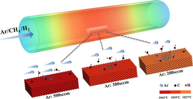
Taking the calculated results into account, the mechanism of ARM graphene synthesis is illustrated as shown in Figure 8. The three Ar flow rates in the experiment were represented by different numbers of Ar molecules at the inlet of the quartz tube. The velocity of the Ar stream was represented by the length of the molecular tail, and consistent CH4 and H2 flows were carried by Ar flow to the substrate surface. At the beginning of graphene growth, the Ar flow rate was set to 500 sccm, and the temperature of the substrate surface was higher (1042 °C), as shown in Figure 2c. Although the thickness of the boundary layer was relatively thin (3.03 cm), the CH4 molecules in the gas stream were diluted to a greater extent, corresponding to a lower C deposition rate, which was conducive to reducing the nucleation sites of graphene. According to the Arrhenius formula, K is affected by the temperature of the system. When the Ar flow rate was reduced to 300 sccm, the substrate surface temperature decreased to 1035 °C, accompanied by a reduction in the K from 0.108 to 0.096 s–1, and the thickness of δ increased from 3.03 to 3.16 cm, which inhibited graphene multipoint nucleation. In addition, the C deposition rate increased, and active carbon atoms would preferentially attach to the edges of nucleated graphene domains. As the Ar flow rate reduced to 200 sccm, the mixed gas flow in the tube was gentle, and the substrate surface temperature was decreased to 1027 °C; the K value reduced to 0.083 s–1, and the thickness of δ was further elevated to 3.31 cm, which were beneficial for maintaining a lower nucleation density and preventing connection into polycrystalline films. Meanwhile, a larger C deposition rate shown in Table 1 derived from higher CH4 concentrations provided a sufficient driving force for graphene domain expansion. In consequence, the proposed ARM is available for breaking the reaction cessation existing in a common consistent method.
Figure 8.
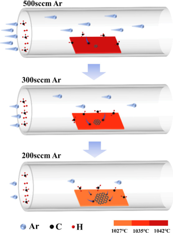
Schematic diagram of graphene prepared by ARM.
Conclusions
In summary, the effect of Ar on temperature and flow fields was revealed based on the different physical parameters of the gases involved in graphene growth. Both experimental characterization and numerical simulation demonstrated that the temperature and gas flow rate within the reaction system became lower as the Ar flow rate decreased. CFD simulation proved that when the Ar flow rate decreased from 500 to 100 sccm, the C deposition rates increased by 1.5 times, which is attributed to the diluting effect of Ar on CH4. By dynamic regulation of the Ar flow rate, and the growth habit of graphene was optimized. As the gradient descent of the Ar flow rate from 500 to 200 sccm by an ARM graphene growth, the nucleation density on polycrystalline Cu substrates is suppressed, while the graphene growth rate is dramatically increased. Millimeter-scale monocrystalline graphene with high mechanical strength (821 GPa Young’s modulus) was prepared. Multitudinous characterizations confirm that the grown graphene was of high crystalline quality. The proposed ARM in this work may provide a new idea for the preparation of high-quality graphene and other two-dimensional materials.
Acknowledgments
This work was supported by funding Shandong Provincial Youth Innovation Science and Technology Support Program for Colleges and Universities (2022KJ032), the Key R&D Plan of Shandong University (2022ZLGX02), the Shandong Provincial Natural Science Foundation (ZR2024QE463), the Natural Science Foundation of Shandong Province (ZR2022MF229), and the Open Project of State Key Laboratory of Crystal Materials, Shandong University (KF2014).
Supporting Information Available
The Supporting Information is available free of charge at https://pubs.acs.org/doi/10.1021/acsomega.4c06728.
OM images of graphene samples under different Ar flow rates; OM images of graphene prepared by three Ar regulation methods; and SEM images of the monocrystalline graphene domain (PDF)
The authors declare no competing financial interest.
Supplementary Material
References
- Ganguli A.; Faramarzi V.; Mostafa A.; Hwang M. T.; You S.; Bashir R. High sensitivity graphene field effect transistor-based detection of DNA amplification. Adv. Funct. Mater. 2020, 30 (28), 2001031. 10.1002/adfm.202001031. [DOI] [Google Scholar]
- Cao M.-S.; Wang X.-X.; Cao W.-Q.; Yuan J. Ultrathin graphene: electrical properties and highly efficient electromagnetic interference shielding. J. Mater. Chem. C 2015, 3 (26), 6589–6599. 10.1039/C5TC01354B. [DOI] [Google Scholar]
- Morozov S. V.; Novoselov K. S.; Katsnelson M. I.; Schedin F.; Elias D. C.; Jaszczak J. A.; Geim A. K. Giant intrinsic carrier mobilities in graphene and its bilayer. Phys. Rev. Lett. 2008, 100 (1), 016602. 10.1103/PhysRevLett.100.016602. [DOI] [PubMed] [Google Scholar]
- Balandin A. A. Thermal properties of graphene and nanostructured carbon materials. Nat. Mater. 2011, 10 (8), 569–581. 10.1038/nmat3064. [DOI] [PubMed] [Google Scholar]
- Papageorgiou D. G.; Kinloch I. A.; Young R. J. Mechanical properties of graphene and graphene-based nanocomposites. Prog. Mater. Sci. 2017, 90, 75–127. 10.1016/j.pmatsci.2017.07.004. [DOI] [Google Scholar]
- Deng B.; Hou Y.; Liu Y.; Khodkov T.; Goossens S.; Tang J.; Wang Y.; Yan R.; Du Y.; Koppens F. H. L.; et al. Growth of ultraflat graphene with greatly enhanced mechanical properties. Nano Lett. 2020, 20 (9), 6798–6806. 10.1021/acs.nanolett.0c02785. [DOI] [PubMed] [Google Scholar]
- Bruna M.; Borini S. Optical constants of graphene layers in the visible range. Appl. Phys. Lett. 2009, 94 (3), 031901. 10.1063/1.3073717. [DOI] [Google Scholar]
- Raccichini R.; Varzi A.; Passerini S.; Scrosati B. The role of graphene for electrochemical energy storage. Nat. Mater. 2015, 14 (3), 271–279. 10.1038/nmat4170. [DOI] [PubMed] [Google Scholar]
- Shangguan Q.; Chen Z.; Yang H.; Cheng S.; Yang W.; Yi Z.; Wu X.; Wang S.; Yi Y.; Wu P. Design of ultra-narrow band graphene refractive index sensor. Sensors 2022, 22, 6483. 10.3390/s22176483. [DOI] [PMC free article] [PubMed] [Google Scholar]
- Novoselov K. S.; Geim A. K.; Morozov S. V.; Jiang D.; Zhang Y.; Dubonos S. V.; Grigorieva I. V.; Firsov A. A. Electric field effect in atomically thin carbon films. Science 2004, 306 (5696), 666–669. 10.1126/science.1102896. [DOI] [PubMed] [Google Scholar]
- Mohan V. B.; Lau K.-t.; Hui D.; Bhattacharyya D. Graphene-based materials and their composites: A review on production, applications and product limitations. Composites, Part B 2018, 142, 200–220. 10.1016/j.compositesb.2018.01.013. [DOI] [Google Scholar]
- Akinwande D.; Huyghebaert C.; Wang C. H.; Serna M. I.; Goossens S.; Li L. J.; Wong H. P.; Koppens F. H. L. Graphene and two-dimensional materials for silicon technology. Nature 2019, 573 (7775), 507–518. 10.1038/s41586-019-1573-9. [DOI] [PubMed] [Google Scholar]
- Zhao J.; Ji P.; Li Y.; Li R.; Zhang K.; Tian H.; Yu K.; Bian B.; Hao L.; Xiao X.; et al. Ultrahigh-mobility semiconducting epitaxial graphene on silicon carbide. Nature 2024, 625 (7993), 60–65. 10.1038/s41586-023-06811-0. [DOI] [PubMed] [Google Scholar]
- Novoselov K. S.; Geim A. K.; Morozov S. V.; Jiang D.; Katsnelson M. I.; Grigorieva I. V.; Dubonos S. V.; Firsov A. A. Two-dimensional gas of massless Dirac fermions in graphene. Nature 2005, 438 (7065), 197–200. 10.1038/nature04233. [DOI] [PubMed] [Google Scholar]
- Zhang J.; Lin L.; Jia K.; Sun L.; Peng H.; Liu Z. Controlled growth of single-crystal graphene films. Adv. Mater. 2020, 32 (1), 1903266. 10.1002/adma.201903266. [DOI] [PubMed] [Google Scholar]
- Choi S. H.; Yun S. J.; Won Y. S.; Oh C. S.; Kim S. M.; Kim K. K.; Lee Y. H. Large-scale synthesis of graphene and other 2D materials towards industrialization. Nat. Commun. 2022, 13 (1), 1484. 10.1038/s41467-022-29182-y. [DOI] [PMC free article] [PubMed] [Google Scholar]
- Quellmalz A.; Wang X.; Sawallich S.; Uzlu B.; Otto M.; Wagner S.; Wang Z.; Prechtl M.; Hartwig O.; Luo S.; et al. Large-area integration of two-dimensional materials and their heterostructures by wafer bonding. Nat. Commun. 2021, 12 (1), 917. 10.1038/s41467-021-21136-0. [DOI] [PMC free article] [PubMed] [Google Scholar]
- Li X. S.; Cai W. W.; An J. H.; Kim S.; Nah J.; Yang D. X.; Piner R.; Velamakanni A.; Jung I.; Tutuc E.; et al. Large-area synthesis of high-quality and uniform graphene films on copper foils. Science 2009, 324 (5932), 1312–1314. 10.1126/science.1171245. [DOI] [PubMed] [Google Scholar]
- Wang M.; Huang M.; Luo D.; Li Y.; Choe M.; Seong W. K.; Kim M.; Jin S.; Wang M.; Chatterjee S.; et al. Single-crystal, large-area, fold-free monolayer graphene. Nature 2021, 596 (7873), 519–524. 10.1038/s41586-021-03753-3. [DOI] [PubMed] [Google Scholar]
- Zhang X.; Guo X.; Sun X. C.; Su Z.; Sun L.; Wang P.; Li Y. L.; Yu F. P.; Zhao X. Roles of CuO and Cu2O in graphene growth on a copper substrate. Appl. Surf. Sci. 2022, 576, 151812. 10.1016/j.apsusc.2021.151812. [DOI] [Google Scholar]
- Li X.; Colombo L.; Ruoff R. S. Synthesis of graphene films on copper foils by chemical vapor deposition. Adv. Mater. 2016, 28 (29), 6247–6252. 10.1002/adma.201504760. [DOI] [PubMed] [Google Scholar]
- Sun L.; Yuan G.; Gao L.; Yang J.; Chhowalla M.; Gharahcheshmeh M. H.; Gleason K. K.; Choi Y. S.; Hong B. H.; Liu Z. Chemical vapour deposition. Nat. Rev. Methods Primers 2021, 1 (1), 5. 10.1038/s43586-020-00005-y. [DOI] [Google Scholar]
- Vlassiouk I. V.; Stehle Y.; Pudasaini P. R.; Unocic R. R.; Rack P. D.; Baddorf A. P.; Ivanov I. N.; Lavrik N. V.; List F.; Gupta N.; et al. Evolutionary selection growth of two-dimensional materials on polycrystalline substrates. Nat. Mater. 2018, 17 (4), 318–322. 10.1038/s41563-018-0019-3. [DOI] [PubMed] [Google Scholar]
- Chen C. Y.; Dai D.; Chen G. X.; Yu J. H.; Nishimura K.; Lin C. T.; Jiang N.; Zhan Z. L. Rapid growth of single-layer graphene on the insulating substrates by thermal CVD. Appl. Surf. Sci. 2015, 346, 41–45. 10.1016/j.apsusc.2015.03.204. [DOI] [Google Scholar]
- Li X. S.; Cai W. W.; Colombo L.; Ruoff R. S. Evolution of Graphene Growth on Ni and Cu by Carbon Isotope Labeling. Nano Lett. 2009, 9 (12), 4268–4272. 10.1021/nl902515k. [DOI] [PubMed] [Google Scholar]
- Geng D. C.; Wang H. P.; Yu G. Graphene single crystals: Size and morphology engineering. Adv. Mater. 2015, 27 (18), 2821–2837. 10.1002/adma.201405887. [DOI] [PubMed] [Google Scholar]
- Ma R.; Huan Q.; Wu L.; Yan J.; Guo W.; Zhang Y. Y.; Wang S.; Bao L.; Liu Y.; Du S.; et al. Direct four-probe measurement of grain-boundary resistivity and mobility in millimeter-sized graphene. Nano Lett. 2017, 17 (9), 5291–5296. 10.1021/acs.nanolett.7b01624. [DOI] [PubMed] [Google Scholar]
- Wu J.; Li Y.; Pan D.; Jiang C.; Jin C.; Song F.; Wang G.; Wan J. Effect of grain boundaries on charge transport in CVD-grown bilayer graphene. Carbon 2019, 147, 434–440. 10.1016/j.carbon.2019.03.029. [DOI] [Google Scholar]
- Luo D.; Wang M.; Li Y.; Kim C.; Yu K. M.; Kim Y.; Han H.; Biswal M.; Huang M.; Kwon Y.; et al. Adlayer-free large-area single crystal graphene grown on a Cu(111) foil. Adv. Mater. 2019, 31 (35), 1903615. 10.1002/adma.201903615. [DOI] [PubMed] [Google Scholar]
- Wang Y.; Qing F.; Jia Y.; Duan Y.; Shen C.; Hou Y.; Niu Y.; Shi H.; Li X. Synthesis of large-area graphene films on rolled-up Cu foils by a “breathing” method. Chem. Eng. J. 2021, 405, 127014. 10.1016/j.cej.2020.127014. [DOI] [Google Scholar]
- Zhang X. F.; Wu T. R.; Jiang Q.; Wang H. S.; Zhu H. L.; Chen Z. Y.; Jiang R.; Niu T. C.; Li Z. J.; Zhang Y. W.; et al. Epitaxial Growth of 6 in. Single-Crystalline Graphene on a Cu/Ni (111) Film at 750 °C via Chemical Vapor Deposition. Small 2019, 15 (22), 1805395. 10.1002/smll.201805395. [DOI] [PubMed] [Google Scholar]
- Deng B.; Liu Z.; Peng H. Toward mass production of CVD graphene films. Adv. Mater. 2019, 31 (9), 1800996. 10.1002/adma.201800996. [DOI] [PubMed] [Google Scholar]
- Zhang Y.; Zhang H.; Li F.; Shu H.; Chen Z.; Sui Y.; Zhang Y.; Ge X.; Yu G.; Jin Z.; et al. Invisible growth of microstructural defects in graphene chemical vapor deposition on copper foil. Carbon 2016, 96, 237–242. 10.1016/j.carbon.2015.09.041. [DOI] [Google Scholar]
- Lin L.; Sun L.; Zhang J.; Sun J.; Koh A. L.; Peng H.; Liu Z. Rapid growth of large single-crystalline graphene via second passivation and multistage carbon supply. Adv. Mater. 2016, 28 (23), 4671–4677. 10.1002/adma.201600403. [DOI] [PubMed] [Google Scholar]
- Wu T.; Zhang X.; Yuan Q.; Xue J.; Lu G.; Liu Z.; Wang H.; Wang H.; Ding F.; Yu Q.; et al. Fast growth of inch-sized single-crystalline graphene from a controlled single nucleus on Cu-Ni alloys. Nat. Mater. 2016, 15 (1), 43–47. 10.1038/nmat4477. [DOI] [PubMed] [Google Scholar]
- Ding D.; Solís-Fernández P.; Yunus R. M.; Hibino H.; Ago H. Behavior and role of superficial oxygen in Cu for the growth of large single-crystalline graphene. Appl. Surf. Sci. 2017, 408, 142–149. 10.1016/j.apsusc.2017.02.250. [DOI] [Google Scholar]
- Su Z.; Sun X.; Liu X.; Zhang J.; Sun L.; Zhang X.; Liu Z.; Yu F.; Li Y.; Cheng X.; et al. A strategy to prepare high-quality monocrystalline graphene: Inducing graphene growth with seeding chemical vapor deposition and Its mechanism. ACS Appl. Mater. Interfaces 2020, 12 (1), 1306–1314. 10.1021/acsami.9b16549. [DOI] [PubMed] [Google Scholar]
- Chaitoglou S.; Bertran E. Effect of temperature on graphene grown by chemical vapor deposition. J. Mater. Sci. 2017, 52 (13), 8348–8356. 10.1007/s10853-017-1054-1. [DOI] [Google Scholar]
- Huet B.; Raskin J.-P. Pressure-controlled chemical vapor deposition of single-layer graphene with millimeter-size domains on thin copper film. Chem. Mater. 2017, 29 (8), 3431–3440. 10.1021/acs.chemmater.6b04928. [DOI] [Google Scholar]
- Wu T.; Ding G.; Shen H.; Wang H.; Sun L.; Jiang D.; Xie X.; Jiang M. Triggering the continuous growth of graphene toward millimeter-sized grains. Adv. Funct. Mater. 2013, 23 (2), 198–203. 10.1002/adfm.201201577. [DOI] [Google Scholar]
- Huang M.; Deng B.; Dong F.; Zhang L.; Zhang Z.; Chen P. Substrate engineering for CVD growth of single crystal graphene. Small Methods 2021, 5 (5), 2001213. 10.1002/smtd.202001213. [DOI] [PubMed] [Google Scholar]
- Hedayat S. M.; Karimi-Sabet J.; Shariaty-Niassar M. Evolution effects of the copper surface morphology on the nucleation density and growth of graphene domains at different growth pressures. Appl. Surf. Sci. 2017, 399, 542–550. 10.1016/j.apsusc.2016.12.126. [DOI] [Google Scholar]
- Kostogrud I. A.; Trusov K. V.; Smovzh D. V. Influence of gas mixture and temperature on AP-CVD synthesis of graphene on copper foil. Adv. Mater. Interfaces 2016, 3 (8), 1500823. 10.1002/admi.201500823. [DOI] [Google Scholar]
- Huet B.; Raskin J. P. Role of Cu foil in-situ annealing in controlling the size and thickness of CVD graphene domains. Carbon 2018, 129, 270–280. 10.1016/j.carbon.2017.12.043. [DOI] [Google Scholar]
- Li X.; Magnuson C. W.; Venugopal A.; An J.; Suk J. W.; Han B.; Borysiak M.; Cai W.; Velamakanni A.; Zhu Y.; et al. Graphene films with large domain size by a two-step chemical vapor deposition process. Nano Lett. 2010, 10 (11), 4328–4334. 10.1021/nl101629g. [DOI] [PubMed] [Google Scholar]
- Eres G.; Regmi M.; Rouleau C. M.; Chen J. H.; Ivanov I. N.; Puretzky A. A.; Geohegan D. B. Cooperative island growth of large-area single-crystal graphene on copper using chemical vapor deposition. ACS Nano 2014, 8 (6), 5657–5669. 10.1021/nn500209d. [DOI] [PubMed] [Google Scholar]
- Vlassiouk I.; Regmi M.; Fulvio P. F.; Dai S.; Datskos P.; Eres G.; Smirnov S. Role of hydrogen in chemical vapor deposition growth of large single-crystal graphene. ACS Nano 2011, 5 (7), 6069–6076. 10.1021/nn201978y. [DOI] [PubMed] [Google Scholar]
- Xiao R.; Luo Q.; Cao Z.; Tian C.; Wang S.; Zhao S.; Zhang G.; Li Z.; Zhang Y.; Shu H.; et al. Hydrogen-modulation method for wafer-scale few-layer single-crystal graphene growth. Carbon 2023, 213, 118289. 10.1016/j.carbon.2023.118289. [DOI] [Google Scholar]
- Chen C.-C.; Kuo C.-J.; Liao C.-D.; Chang C.-F.; Tseng C.-A.; Liu C.-R.; Chen Y.-T. Growth of large-area graphene single crystals in confined reaction space with diffusion-driven chemical vapor deposition. Chem. Mater. 2015, 27 (18), 6249–6258. 10.1021/acs.chemmater.5b01430. [DOI] [Google Scholar]
- Huang M.; Bakharev P. V.; Wang Z. J.; Biswal M.; Yang Z.; Jin S.; Wang B.; Park H. J.; Li Y.; Qu D.; et al. Large-area single-crystal AB-bilayer and ABA-trilayer graphene grown on a Cu/Ni(111) foil. Nat. Nanotechnol. 2020, 15 (4), 289–295. 10.1038/s41565-019-0622-8. [DOI] [PubMed] [Google Scholar]
- Lee C.; Wei X. D.; Kysar J. W.; Hone J. Measurement of the elastic properties and intrinsic strength of monolayer graphene. Science 2008, 321 (5887), 385–388. 10.1126/science.1157996. [DOI] [PubMed] [Google Scholar]
- Lewis A. M.; Derby B.; Kinloch I. A. Influence of gas phase equilibria on the chemical vapor deposition of graphene. ACS Nano 2013, 7 (4), 3104–3117. 10.1021/nn305223y. [DOI] [PubMed] [Google Scholar]
- Lin L.; Deng B.; Sun J. Y.; Peng H. L.; Liu Z. F. Bridging the gap between reality and ideal in chemical vapor deposition growth of graphene. Chem. Rev. 2018, 118 (18), 9281–9343. 10.1021/acs.chemrev.8b00325. [DOI] [PubMed] [Google Scholar]
- Kim H.; Mattevi C.; Calvo M. R.; Oberg J. C.; Artiglia L.; Agnoli S.; Hirjibehedin C. F.; Chhowalla M.; Saiz E. Activation energy paths for graphene nucleation and growth on Cu. ACS Nano 2012, 6 (4), 3614–3623. 10.1021/nn3008965. [DOI] [PubMed] [Google Scholar]
Associated Data
This section collects any data citations, data availability statements, or supplementary materials included in this article.


