

Abstract
This paper proposed a hybrid switched-capacitor inverter to reduce the number of components and achieve automatic capacitor balancing. The proposed structure combines a switched capacitor (SC) unit with a flying capacitor (FC). Significant advantages of the proposed design include a reduced number of components, simple control, voltage boosting capability, and limitation of the inrush current during capacitor charging. The proposed structure used only eleven switches and three capacitors to generate 13 levels. Compared to other 13-level switched-capacitor inverters, the proposed structure utilizes fewer components, capacitors with lower maximum voltage, and fewer conduction components. The flying capacitor used in the proposed design can naturally balance at half of the input DC voltage (0.5Vdc), enabling sensor-free operation. Therefore, with simple control over the inherent voltage balancing of the capacitors, the structure requires only six switching signals, which reduces the overall system cost. Circuit performance analysis, automatic capacitor balancing, and the charging and discharging processes are introduced. Subsequently, a numerical comparison is made with recently proposed 13-level switched-capacitor inverters, demonstrating the advantages of reduced active components, simplified control, cost-effectiveness, and low power losses. Finally, simulation results are presented to confirm the performance of the proposed structure.
Keywords: Multilevel inverter, Switched capacitor, Voltage boosting, Automatic balancing, Reduced components, Inrush current limitation
Subject terms: Engineering, Electrical and electronic engineering
Introduction
Recently, the emergence of multilevel inverters (MLIs) has provided extensive solutions for DC/AC electrical energy conversion systems1. The advantages of multilevel inverters include improved output voltage with low total harmonic distortion (THD), reduced voltage stress on switches, less need for filters, low dv/dt stress, and high modularity. These features make this type of inverter suitable for applications such as connecting renewable energy sources to the grid, electric vehicles, and other distributed AC generation systems2. Conventional inverters are generally divided into three categories: Cascaded H-Bridge (CHB), Neutral Point Clamped (NPC), and Flying Capacitors (FCs). The conventional inverters mentioned have applications in some industrial fields. However, there are drawbacks associated with these inverters. The CHB structure requires isolated DC sources and expensive, bulky phase-shifting transformers. The flying capacitor structure requires many DC capacitors, which leads to the problem of capacitor voltage balancing. NPC inverters also need a large number of diodes to achieve higher levels. The complexity of controlling the DC link capacitor voltage balance with conventional modulation techniques also emerges as a significant issue3.
Various research efforts have been undertaken to address the shortcomings of conventional multilevel structures. Reference4 reported a multilevel structure that cannot attributed to traditional inverters. Compared to conventional multilevel inverters, these structures can produce more voltage levels with fewer switches. The hybrid modulation method used additional switching states to balance the capacitor voltages. However, they inevitably require sensors for voltage/current detection, which increases system costs and control complexity. The 11-level structure in5 features automatic balancing and requires 12 switches and four capacitors. The switches control the capacitors operating status to enable the conversion and transfer of electrical energy.
In some structures, DC-AC voltage conversion is performed using an H-bridge circuit, while the switches in the H-bridge must withstand the maximum output voltage6. The structure in7 inherently can change the polarity of the output voltage without the need for an H-bridge module, thereby reducing the voltage stress on the switches. The maximum capacitor voltage stress in the 13-level switched capacitor inverter presented in8 is one-third of the maximum output voltage. Although this structure has a high boosting factor, it has many components. In the 13-level structure of9, the maximum capacitor voltage is one-sixth of the maximum output voltage, yet it still has many components. In the structure from10, the maximum voltage stress on the semiconductors is half of the maximum output voltage. While the boosting factor is high, the number of components and the maximum capacitor voltage stress are high, and a high-voltage capacitor is required. Also, the eight switches’ voltage stress is half the maximum output voltage. In the 13-level structure presented in11, the maximum capacitor voltage is one-sixth of the maximum output voltage and requires nine switching signals. However, this structure needs two input sources and also has a large number of components. Moreover, the structure in12, despite reducing the voltage stress on the structural elements, has many complex control signals and a higher average of conduction devices across more levels.
Inrush current is one of the significant challenges in developing multilevel switched-capacitor inverters, and failure to limit it can cause stress on the inverter components. One method to reduce inrush current is to add an inductor unit in parallel with a diode, with its value determined based on the maximum continuous discharge time and the capacitance of the relevant capacitor13,14. In the 17-level structure of9, the inrush current has been reduced using inductance in series with the source. However, this structure has 14 switches and two diodes and requires a high-voltage level capacitor. The 13-level structure of14 utilized additional switching states, reducing voltage ripple and inrush current during capacitor charging. However, this structure has a large number of components and also requires a high-voltage level capacitor. Despite reducing the maximum voltage stress on the components, nine of the switches still endure the maximum voltage stress, which leads to an increase in the total switching voltage (TSV).
This paper proposes a structure that generates a 13-level output voltage with only 11 switches and three capacitors. The proposed structure requires minimal signals for the switch drivers and does not require high-voltage capacitors. Additionally, the average number of active components needed to generate each voltage level is meager, resulting in minimal conduction losses for the switching devices. In this structure, using a limiting inductor unit reduced the inrush current. The structure of the subsequent sections of the paper is as follows. Section “Proposed structure” explains the proposed circuit structure, operating states, proposed modulation scheme, balancing analysis, and capacitor design. Section “Component stress analysis” analyzes current stress, determines the limiting inductor value, and determines voltage stress on the components. Section “Loss calculation” examined the losses. Section “Comparative evaluation” presents the analysis and comparative study of the proposed structure with recent switched capacitor multilevel inverters. Section “Results and discussion” provided simulation and experimental results. Finally, Sect. 8 presented the conclusion.
Proposed structure
Structure and operation of the proposed topology
The proposed structure, as shown in Fig. 1, includes 11 switches (Sa, Sʹa, …, Sc, Sʹc) and three capacitors (C1–C3), with the maximum capacitor voltage being one-third of the maximum output voltage. This structure consists of a threefold multiplier section and a flying capacitor branch, which has a boosting factor of 3.
Fig. 1.
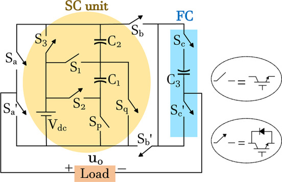
Proposed 13-level inverter structure.
The input DC source voltage (Vdc) charged capacitors C1 and C2 separately; the voltage across capacitor C3 is half the input voltage (0.5Vdc). The proposed structure needs 6 gate signals for switching. The most minor state changes occur in a switching period for Sb and Sʹb. The remaining switches also experience minimal state changes. According to the switching states listed in Table 1, the values “1” and “0” correspond to the on and off states of the switches, respectively. Table 1 also shows the number of devices conducted for each level. According to Table 1, three semiconductors conduct at two levels, four semiconductors conduct at three levels, and five switches conduct at eight levels, which is a reasonable amount compared to similar structures. The number of active devices at each level directly impacts conduction losses. The average number of semiconductors conducting at each level is 4.4 devices, which is very suitable and low compared to similar structures.
Table 1.
Switching logic for generating different levels in the proposed structure.
| Level | Sa | Sb | Sc | S1, Sp | S2 | S3, Sq | Active switches |
|---|---|---|---|---|---|---|---|
| + 3Vdc | 1 | 0 | 0 | 0 | 1 | 0 | Sc’, Sb’, S2, Sa |
| + 2.5Vdc | 1 | 0 | 1 | 0 | 1 | 0 | Sc, Sb’, S2, Sa |
| + 2Vdc | 1 | 0 | 0 | 1 | 0 | 0 | Sc’, Sb’, S1, Sp, Sa |
| + 1.5Vdc | 1 | 0 | 1 | 1 | 0 | 0 | Sc, Sb’, S1, Sp, Sa |
| + Vdc | 1 | 0 | 0 | 0 | 0 | 1 | Sc’, Sb’, Sq, S3, Sa |
| + 0.5Vdc | 1 | 0 | 1 | 0 | 0 | 1 | Sc, Sb’, Sq, S3, Sa |
| 0 | 0 | 0 | 0 | 0 | 0 | 0 | Sc’, Sb’, Sa’ |
| − 0.5Vdc | 1 | 1 | 1 | 0 | 0 | 0 | Sa, Sb, Sc |
| − Vdc | 0 | 1 | 0 | 0 | 0 | 1 | Sa’, Sb, Sc’, Sq, S3 |
| − 1.5Vdc | 0 | 1 | 1 | 0 | 0 | 1 | Sa’, Sb, Sc, Sq, S3 |
| − 2Vdc | 0 | 1 | 0 | 1 | 0 | 0 | Sc’, Sb, S1, Sp, Sa’ |
| − 2.5Vdc | 0 | 1 | 1 | 1 | 0 | 0 | Sc, Sb, S1, Sp, Sa’ |
| − 3Vdc | 0 | 1 | 0 | 0 | 1 | 0 | Sc’, Sb, S2, Sa’ |
Table 2 shows the number of state changes in the control signals of the switches required to create the next level. This parameter directly affects switching losses and control simplicity. According to Table 2, the average number of state changes in the signals during level transitions is 2.1, which is very reasonable and results in lower switching losses and more straightforward control in the proposed structure.
Table 2.
Number of state changes in the control signals of the switches for level change.
| Level change | − 3 − 2.5 |
− 2.5 − 2 |
− 2 − 1.5 |
− 1.5 − 1 |
− 1 − 0.5 |
− 0.5 0 |
0 0.5 |
0.5 1 |
1 1.5 |
1.5 2 |
2 2.5 |
2.5 3 |
|---|---|---|---|---|---|---|---|---|---|---|---|---|
| The number of state changes in the control signals | 3 | 1 | 3 | 1 | 3 | 3 | 3 | 1 | 3 | 1 | 3 | 1 |
Operating states
Figure 2 shows the different conduction states of the devices for generating the desired levels during the positive half-period. The blue line represents the path for powering the load through the source and capacitors, while the green line indicates the path for charging the capacitors. The modulation scheme controls the switch gate to maintain the capacitor voltage balance during level generation, and the capacitor voltage ripple remains within an acceptable range of less than 10 percent.
Fig. 2.

Device conduction states for generating levels during the positive half-period.
Modified phase shift modulation
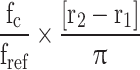
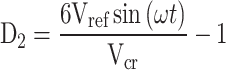
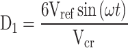
The proposed structure used sinusoidal pulse width modulation (SPWM) to create the switching pattern for the proposed 13-level inverter. The switching behavior and the on/off states of the seven control signals for the ten switches of the proposed inverter and the capacitor voltage ripple are shown in Fig. 3. According to this Figure, the proposed modulation method automatically balances the capacitor voltages. The balanced voltages of capacitors C1, C2, and C3 are Vdc, Vdc, and 0.5Vdc, respectively. For the phase shift modulation in the proposed multilevel inverter, a comparison is made between a reference sinusoidal waveform with a maximum value of one and 12 carriers with the same frequency and amplitude but with phase shifts. Equation (1) shows the phase difference between the carriers, and Eq. (2) illustrates the relationship between the inverter frequency, the component frequencies, and the phase-shifted carrier switching frequency. In these equations, k represents the number of carrier signals required, φcr is the phase of the carrier signals, fsw,inv is the equivalent switching frequency of the inverter and fsw,dev is the switching frequency of the components of the structure.
Fig. 3.
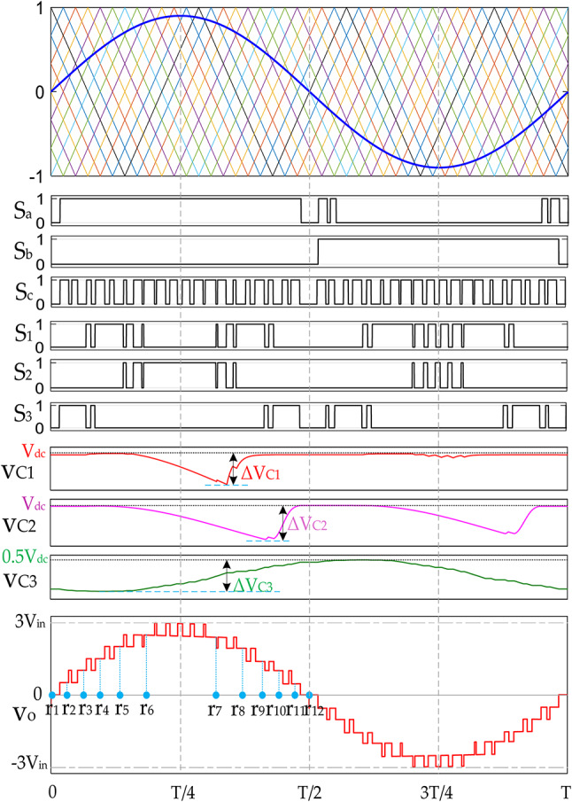
Modulation of the proposed structure.
 |
1 |
 |
2 |
According to Fig. 3, switches Sa and Sʹa and Sb and Sʹb experience the least stress, while switches Sc and Sʹc are subjected to higher switching stress than the other switches in the structure.
Capacitor balancing
Figure 4 and Table 3 show the charging and discharging patterns of the capacitors. Charging and discharging periods ensured The automatic balancing of the capacitors. Capacitor C3 is charged during the positive half-period and discharged during the negative half-period, with equal charging and discharging durations. This capacitor is initially connected to a pre-charging circuit and charged to the required voltage, after which it can be used easily. The voltage balance of the other two capacitors in the structure is maintained through appropriate charging and discharging during level generation using the proposed modulation, with a permissible voltage ripple of less than 10 percent. State “C” indicates the charging condition, and ”D” represents discharging. The guiding components in the capacitor’s charging loop at each level are also specified. At levels 0 and − 0.5, capacitors C1 and C2 are in a no-change (N) state, meaning they are neither charged nor discharged, and the load path is established through the half-bridges or along with the capacitor in series with the switch (C3).
Fig. 4.

Charging and discharging patterns of capacitors.
Table 3.
Charging and discharging patterns of capacitors.
| Level | Charge loop switches | C1 | C2 | C3 |
|---|---|---|---|---|
| + 3 | – | D | D | N |
| + 2.5 | – | D | D | D |
| + 2 | S1, Sp | C | D | N |
| + 1.5 | S1, Sp | C | D | D |
| + 1 | Sq, S3 | N | C | N |
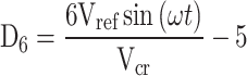
| + 0.5 | Sq, S3 | N | C | D |
| 0 | – | N | N | N |
| − 0.5 | – | N | N | C |
| − 1 | Sq, S3 | N | C | N |
| − 1.5 | Sq, S3 | N | C | C |
| − 2 | S1, Sp | C | D | N |
| − 2.5 | S1, Sp | C | D | C |
| − 3 | – | D | D | N |
Appropriate sequences of charging and discharging in each period achieved the automatic voltage balancing of capacitors C1 and C2. Capacitor C3 discharges at levels + Vdc/2, + 3Vdc/2, and + 5Vdc/2, and symmetrically charges at levels − Vdc/2, − 3Vdc/2, and − 5Vdc/2. As a result, the voltage of the flying capacitor C3 automatically balances over one fundamental period. The next part discussed the details and related equations for capacitor balancing. Figure 4 shows the charging and discharging regions of each capacitor.
Balancing of capacitor C3
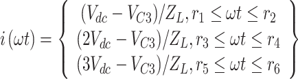
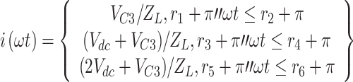
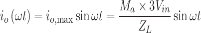
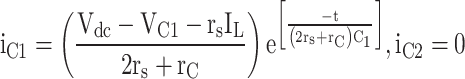
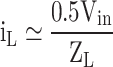
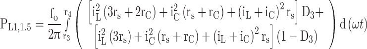
As shown in Fig. 4, Ladder modulation with unit steps can calculate the minimum required capacitance to achieve the desired voltage ripple. The capacitance calculation using ladder modulation represents the worst-case scenario, and the necessary capacitance in pulse width modulation is smaller than that obtained from ladder modulation. Considering ladder modulation, Eq. (3) expressed the load current ZL at levels + Vdc/2, + 3Vdc/2, and + 5Vdc/2. In this equation, i(ωt) represents the load current as a function of time, ω is the angular frequency, and r1 to r6 is the time points corresponding to the changes in the output voltage levels.
 |
3 |
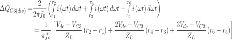
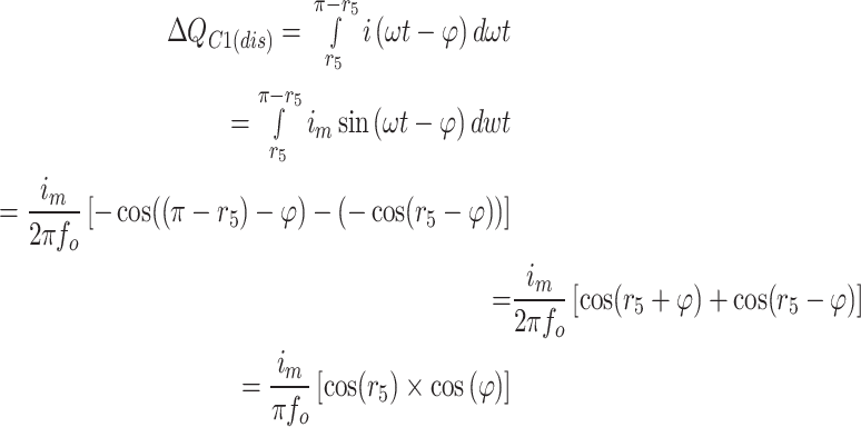
Equation (4) represents the total discharge current of capacitor C3 over one fundamental period. Due to the waveform’s symmetry and the capacitor’s discharge in two-time intervals, 0 to π\2 and π\2 to π, the discharge current for one interval is calculated as half a half-period and doubled. As a result, the total discharge current of capacitor C3 over one fundamental period can be expressed as follows, where fo is the output voltage frequency.
 |
4 |
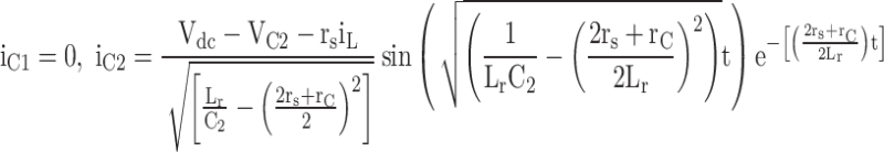
the output load current at negative levels − Vdc/2, -3Vdc/2, and − 5Vdc/2 can be calculated according to Eq. (5).
 |
5 |
The total charge current of capacitor C3 at negative levels during the output period can be expressed according to Eq. (6). Similar to Eq. (4), the calculations in Eq. (6) are performed for half a half- period due to the existing symmetry, and the result is then doubled.
 |
6 |
Equation (7) expresses the total charge of capacitor C3 resulting from charging and discharging over one output period.
 |
7 |
Given that the charge and discharge amounts for the floating capacitor C3 are equal, the primary component of the net charge over one period is effectively zero. Consequently, according to the ampere-second balance law and based on Eq. (7), the voltage of capacitor C3 must be balanced at + Vdc/2.
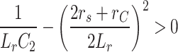
Capacitor design and voltage ripple determination
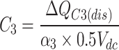
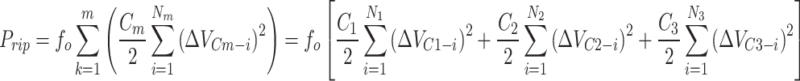
The proposed structure has three capacitors, which can be divided into two design sections: The first consists of the capacitors in the level-building unit (threefold multiplier unit), and the second part includes the series capacitor with the half-bridge switch. For capacitor design, various influencing factors must be considered, including the amount of energy during discharge periods, the allowable voltage ripple of the capacitor, the input voltage, the load impedance, and the modulation index. The capacitance of C3 can be calculated according to Eq. (8), where α3 represents the permissible percentage of voltage ripple for capacitor C3.
 |
8 |
Capacitor C3 discharges during the positive half-period and charges during the negative half-period. As a result, adding inductance to the load and consequently creating a phase shift in the current waveform relative to the voltage does not significantly affect the value of this capacitor. As shown in Fig. 4, the discharge load is first calculated for the two capacitors in the level-building unit, and then the capacity can be determined accordingly. In equations, the phase angle φ considered to obtain a comprehensive relation for different types of output loads. As the load becomes more inductive, this angle approaches 90 degrees. The capacitor values for the level-building unit in the proposed structure have been calculated for a resistive-inductive load. The maximum discharge load of capacitor C1 is calculated based on the maximum discharge time and maximum current, following a similar approach to Eq. (4), as shown in Eq. (9). This calculation is then used to determine the capacitance value in Eq. (10).
 |
9 |
 |
10 |
Calculating the capacitance of capacitor C2 is similar to that of the first capacitor. The maximum discharge charge is calculated in Eq. (11) and then used in Eq. (12) to determine the capacitance of capacitor C2. Capacitor C2 has a longer maximum discharge time than C1 and, therefore, requires a larger capacitance to achieve the same voltage ripple.
 |
11 |
 |
12 |
Figure 5 shows the required capacitance for each capacitor in the structure to achieve specific ripple percentages for a pure resistive load with an input voltage of 100 V and a modulation index of 0.92. The graph plots the voltage ripple percentages ranging from 3 to 10%. According to the calculations, the capacitance ratios for capacitors C1, C2, and C3 for a given voltage ripple are approximately 1:1.7:2.5. As the voltage increases, the percentage of ripple remains unchanged because, according to Eq. (12), the capacitance required for a specific voltage ripple remains constant as the input voltage and output load current increase proportionally.
Fig. 5.

Minimum capacitance requirements for voltage ripple with a pure resistive load.
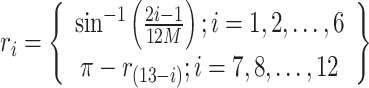
The minimum required capacitance for the specified condition is obtained based on the above relationships. In these relations, α represents the desired voltage ripple, and Vdc is the input link voltage. The timing points for level changes can also be calculated according to relation (13). In this relation, M denotes the modulation index, and ri represents the level change point in Fig. 4.
 |
13 |
Component stress analysis
Current stress analysis
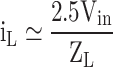
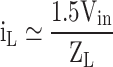
Capacitor C1 is in relatively good condition regarding inrush current due to its appropriate charging periods. In the worst-case scenario, its maximum consecutive discharge occurs across only two levels, resulting in a lower voltage ripple. Assuming the same voltage ripple percentage, C1 has the most negligible capacitance among the three capacitors in the proposed structure. Therefore, increasing the capacitance of this capacitor, which results in a voltage ripple of less than 5%, can significantly reduce the inrush current. Capacitor C2 causes the primary inrush current, as its maximum continuous discharge is greater than that of capacitor C1. Adding a series inductor with switch Sq in the charging loop of this capacitor controls the inrush current. The inrush charging current of the flying capacitor C3 in the proposed structure is practically negligible due to load impedance in its charging path.
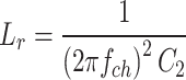
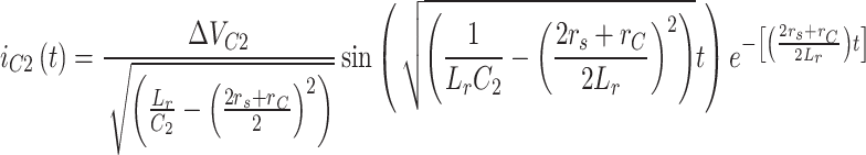
Consequently, this capacitor does not generate an inrush current during charging. The charging circuit of capacitor C1 is illustrated when S1 and Sp are turned on, as shown in Fig. 6a. The equivalent circuit of charging the C2 is depicted during the on and off states of switches S3 and Sq in Fig. 6b and c, respectively. If a small inductor is used in the charging path of capacitor C2, its value for limiting the inrush current of this capacitor can be calculated using Eq. (14). In this equation, fch represents the capacitor charging frequency, and Lr is the required inductance to limit the inrush current of capacitor C215.
 |
14 |
Fig. 6.

Equivalent circuit for the capacitor charging process. (a) Charging circuit for capacitor C1, (b) Charging circuit for capacitor C2, (c) Additional Diode Path, (d) Charging circuit for capacitor C3.
The charging path of capacitor C1 is shown in Fig. 6a. In these figures, the red path corresponds to the typical path for the load and capacitor charging, which, in more precise calculations, causes a voltage drop across the capacitor. Additionally, as shown in Fig. 6b, capacitor C2 is placed in series with Lr during charging, so soft charging occurs when S3 is turned on. In Fig. 6c, when S3 is turned off, the freewheeling diode Dr provides a path for the inductor current, allowing the inductor current to be diverted through the inductor and diode loop to protect the other components of the structure.
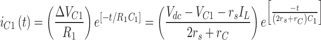
The charging path for capacitor C3 is shown in Fig. 6d. The charging current of capacitor C3 is always equal to the load current since the load impedance is in its path. Despite the appropriate charging sequence of capacitor C1 and the maximum discharge occurring only at two levels, 2.5Vdc and 3Vdc, the charging current of capacitor C1 is limited, as presented in Eq. (15). In this Equation, ΔVC1 represents the voltage ripple of capacitor C1, R1 is the equivalent resistance of the charging loop, and rs and rc are the resistances of the switch and capacitor, respectively.
 |
15 |
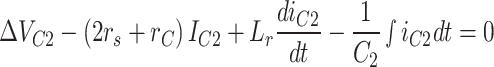
For the current of capacitor C2, the presence of an inductor limits the inrush current. According to Fig. 6b, in the case where the inductor is in the circuit, an RLC circuit is effectively derived from this circuit, and Eq. (16) is derived from this circuit.
 |
16 |
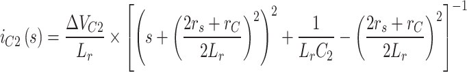
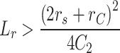
By solving the equation in relation (16) using the Laplace transform, the current response of capacitor C2 is obtained, as shown in relation (17). According to relation (17), the current of capacitor C2 exhibits an overdamped response when the general limits of the parasitic resistances rs and rc of the charging loop, the capacitance of capacitor C2, and the inductance Lr satisfy the condition in relation (18).
 |
17 |
 |
18 |
As a result, the inductance value is determined according to Eqs. (14) and (19). In this case, the instantaneous charging current of capacitor C2, following Eq. (16), exhibits an overdamped response, and its value can be expressed as shown in Eq. (20).
 |
19 |
 |
20 |
Additionally, using Eqs. (21) and (22) and substituting them into Eq. (20), the instantaneous charging current of capacitor C2 simplifies Eq. (23). In these equations, α represents the time constant or damping coefficient, and ω is the damped angular frequency.
 |
21 |
 |
22 |
 |
23 |
Figure 7 shows the inrush current of capacitors C1, C2, and C3 during one main period. In this Figure, with capacitor values of C1 = 1500 µF, C2 = 1800 µF, and C3 = 2200 µF, the maximum ripple percentages are 2.4%, 3.9%, and 4.2% respectively. The inrush current of the capacitors is analyzed with an inductance value of 50 µH. According to this Figure, despite the presence of an inductor in the charging circuit of capacitor C2, the charging current exhibits a damped response, and the inrush current is effectively suppressed. Additionally, capacitor C1, despite having a smaller capacitance and not requiring a limiting inductor in its charging loop, has a relatively low inrush current, indicating no significant need for an inductor in its charging path.
Fig. 7.

Charging currents of the capacitors: Charging current of capacitor C1 (blue curve), charging current of capacitor C2 with limiting inductor (red curve), and charging current of capacitor C3 (brown curve).
Voltage stress analysis
The maximum voltage stress on the proposed structure’s devices is detailed in Table 4. Four switches handle the maximum voltage stress of 3Vdc. Two switches experience a maximum voltage stress of 2Vdc, while three switches and two capacitors endure a maximum voltage stress of Vdc. Additionally, two switches and one capacitor are subjected to a voltage stress of 0.5Vdc. Given the relatively low number of components and the maximum voltage stress on the devices in the proposed structure, capacitors’ total blocking voltage and total voltage are within desirable limits. Consequently, the cost of the devices is expected to be reasonable.
Table 4.
Voltage stress on the components of the proposed structure.
| Semiconductor | Voltage stress |
|---|---|
| Sc, Sc’, C3 | 0.5Vdc |
| S1, Sp, Sq, C1, C2 | Vdc |
| S2, S3 | 2Vdc |
| Sa, Sa’, Sb, Sb’ | 3Vdc |
Loss calculation
In the proposed inverter, similar to other switched capacitor multilevel inverters, charging and discharging the capacitors periodically occurs. During the charging process, losses are mainly due to the voltage ripple of the capacitors. In this case, the capacitor voltage ripple causes the charging current to pass through the parasitic resistance of the charging loop. In the discharge process, losses are mainly due to the load current passing through the parasitic resistances of the discharge loop. Additionally, delays in the switching of the switches also lead to losses. Therefore, the losses in switched capacitor multilevel inverters are categorized into three types: switching losses (Psw), ripple-induced losses (Prip), and conduction losses (Pcond). According to Eq. (24), the total inverter losses are the sum of these three components. In the following section, the losses of the proposed structure are analyzed.
Switching losses
Switching losses occur in a power switch during the on and off processes. During these on-and-off transitions, the voltage across the switch and the current passing through it are non-zero, leading to switching losses in the power switch. Switching losses are evaluated over one main period. When a switch is off and turns on or transitions from on to off, there is a limited time known as the switching delay. toff denotes the switch’s turn-off delay, and the switch’s turn-on delay is denoted by ton. The number of state changes of the switches (NSi) in one main period must be assessed to evaluate switching losses. Table 5 shows the number of state changes for each switch during one main period, based on the switch state transitions according to the information in Table 1.
Table 5.
Number of state changes for each switch in one main period.
| Switch | Number of state changes |
|---|---|
 |
 |
 |
 |
 |
 |
 |
 |
 |
 |
 |
 |
Calculating switching losses requires precise information about the voltage across the switch and the current passing through the switch during the on-time (ton) and off-time (toff) intervals. Analyzing losses based on the switch datasheet can be complex. To simplify the analysis, switching losses are examined using a linear approximation method for the voltage across the switch and the current passing through the switch during the delay times of the turn-on and turn-off processes. Figure 8 illustrates the voltage and current of the switch during the turn-on and turn-off intervals.
Fig. 8.
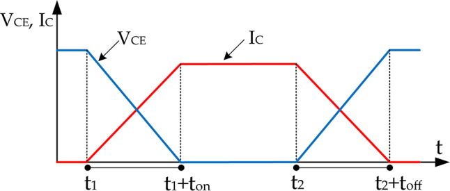
Waveform of voltage and current through the switch during the turn-on and turn-off processes.
Equations (25) and (26) can be used to calculate the switch’s energy losses during the turn-on and turn-off processes, respectively.
 |
24 |
 |
25 |
Given the total number of switch state changes in one main period (NSi) and with reasonable approximation, the number of turn-on (Non) and turn-off (Noff) events can be considered equal and is given by NSi/2, as shown in Eq. (27). To calculate the switching losses of a power switch, the product of the energy dissipated in the switch for each turn-on and turn-off event, multiplied by the number of turn-on and turn-off events and the base frequency, is used according to Eq. (28). By substituting Eqs. (25) and (26) into Eq. (28), the switching loss power of each switch in one main period is obtained according to Eq. (29).
 |
26 |
 |
27 |
 |
28 |
In Eq. (29), the current passing through the power switch is calculated according to Eq. (30) from the sum of the load current at the corresponding level and the charge current.
 |
29 |
Ripple losses
Ripple losses in capacitors arise from the difference between the equilibrium and instantaneous capacitor voltage. These losses depend on the parasitic resistance of the capacitor and its charging path. The ripple voltage of the capacitor is first measured during each continuous discharge period to calculate ripple losses. Then, the amount of ripple loss caused by it is obtained by placing it in the ripple loss equation. The ripple voltages of capacitor Cm for different continuous discharges during the main component’s period are calculated according to the relationship (31). In this Equation, ΔVCm(dis) is the ripple voltage, and ΔQCm(dis) is the discharge load of capacitor Cm. The power loss due to ripple voltage for a capacitor during a single discharge is calculated using Eq. (32). This equation uses the product of the main component frequency and the capacitor’s loss energy. By substituting the ripple values obtained from the discharges of each capacitor over one main component period and aggregating them, the power loss due to the ripple voltage of a capacitor in a switched capacitor structure is obtained according to Eq. (33). In this Equation, Nm represents the number of charging processes of capacitor Cm during one period of the fundamental component.
 |
30 |
 |
31 |
 |
32 |
Conduction losses
Conduction losses arise from the conduction of semiconductor devices such as switches or diodes to create each output voltage level. During the generation of levels, the load current encounters parasitic elements such as the resistance in the switch state (rs), the resistance in the on state of the diode (rd), the forward bias voltage of the diode (Vd), and the internal resistance of the capacitor. (rc). Table 6 shows the equivalent parasitic resistance of the levels in terms of the switch’s on-state resistance and the capacitor’s equivalent resistance, considering the load current and voltage. Figure 9 illustrates the equivalent circuit for creating the levels in the proposed structure. This circuit shows the calculation of conduction losses for each level during the active time of the level in question.
Table 6.
Equivalent parasitic resistance at different levels.
| Output voltage | Parasitic resistance |
|---|---|
 |
 |
 |
 |
 |
 |
 |
 |
 |
 |
Fig. 9.

Equivalent parasitic circuit.
Figure 10 shows the different conduction modes of semiconductor devices to create different voltage levels in the output load. According to this Figure, conduction losses are caused by the passage of load or charge current through parasitic resistances of devices and capacitors. Consequently, both currents must be calculated for different voltage levels.
Fig. 10.

Equivalent circuit of parasitic resistances of circuit devices during the positive half-period of level creation.
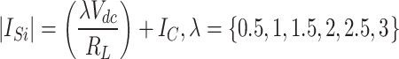
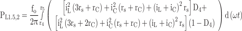
Table 7 specifies the equations for calculating each level’s load current and charging current. Equation (34) calculates the load current, where Ma is the modulation index, and ZL is the load impedance.
 |
33 |
Table 7.
Load current and instantaneous charging current for different positive half-period levels.
| Output voltage | Load current | Charge current |
|---|---|---|
 |
 |
 |
 |
 |
 |
 |
 |
 |
 |
 |
 |
 |
 |
 |
 |
 |
 |
On some levels, the inrush current is suppressed due to the presence of inductors. In other levels where the inductor is not in the capacitor charging path, the ripple voltage of the capacitor is low due to the proper charging sequence, resulting in limited inrush current.
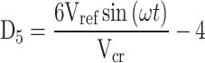
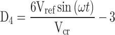
The parasitic resistance of the conducting components at each level and the capacitors in the load or charge path cause conduction losses, and the amount of load current or charging current passing through it is calculated based on the power equation. In these equations, Dk represents the duty period of the k-th level.
Including all four positive and negative half-periods to calculate the conduction losses over a whole period, the total conduction losses calculated from Table 8 are multiplied by 4, as shown in Eq. (35).
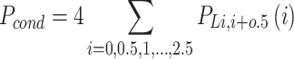 |
34 |
Table 8.
Conduction power losses during switching intervals between two consecutive levels.
| Output voltage | Duty cycle | Conduction losses |
|---|---|---|
 |
 |
 |
 |
 |
 |
 |
 |
 |
 |
 |
 |
 |
 |
 |
 |
 |
 |
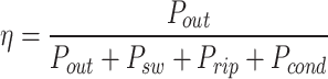
Finally, Eq. (36) can be used to calculate the efficiency of the proposed structure by calculating all the losses in the circuit and having the output power.
 |
35 |
In the following, the loss distribution analysis on the various components of the proposed 13-level switched-capacitor inverter is performed. Therefore, the distribution of losses in each capacitor and switch, including switching, ripple, and conduction losses, is shown in Fig. 11. According to this Figure, the highest percentage of losses in the components of the structure under review occurs in the devices that are part of the capacitor charging loop. In particular, capacitor C2 has a higher voltage ripple than the other two capacitors. Switches Sq and S3, which are in the charging loop of capacitor C2, also have more losses because the charging current of C2 passes through them.
Fig. 11.

Distribution of losses in the components of the proposed structure.
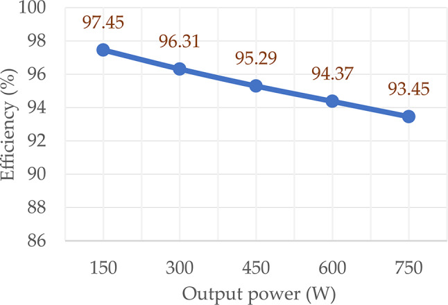
In the following, Fig. 12 shows the efficiency of the proposed inverter for different power levels with an input voltage of 100 V and capacitor values of C1 = 1500 µF, C2 = 1800 µF, and C3 = 2200 µF at various output powers. As shown in the Figure, with increasing output power, the current passing through the semiconductor devices rises, and the proportion of power losses relative to the output power increases. Consequently, the efficiency of the converter decreases. The highest efficiency observed in the tested range is approximately 97.45%.
Fig. 12.
Efficiency chart at different power levels.
Comparative evaluation
This section compares the proposed inverter structure with other recently introduced switched-capacitor inverters. The comparison is based on various parameters, and the results are summarized in Table 9. The structures in references9 and11 have capacitors with a maximum of one-sixth of the peak output voltage. However, they require two DC sources and have many components. The structure in reference8 requires four capacitors and has many control signals for its components, making the control process more complex. The structures in references10 and15 have a gain factor of 6, and the maximum voltage stress on the switches (MBV) is half of the peak output voltage, with a suitable total standing voltage (TSV). However, the number of active components at each level is higher than other structures. Also, the switches that endure the maximum voltage stress include 8 in reference10 and 9 in reference15, which is a relatively high number. Also, the maximum capacitor voltage in the reference structure16 is half of the maximum output voltage, requiring capacitors with a high voltage rating. Reference17 has a relatively low number of switches; however, it includes eight diodes, and its main drawback is the need for two DC input sources. With a single DC source, the proposed structure offers the advantages of having the fewest components (switches, diodes, capacitors) and fewer separate control signals compared to similar structures, making its control implementation simpler.
Table 9.
Comparative evaluation of the proposed structure with similar structures.
| Structure | NSW | NDD | NDr | NC | NComp | NDC | NCo | B | MBVpu | TSVpu | NMBV | VCmax /Vmax | TCDav | CF α = 0.5 |
|---|---|---|---|---|---|---|---|---|---|---|---|---|---|---|
| 8 | 12 | 4 | 11 | 4 | 31 | 1 | 9 | 6 | 0.67 | 5.66 | 2 | 1/3 | 7.1 | 2.6 |
| 9 | 14 | 2 | 14 | 4 | 34 | 2 | 11 | 3 | 1 | 6.66 | 4 | 1/6 | 6.4 | 5.74 |
| 10 | 12 | 4 | 12 | 3 | 31 | 1 | 8 | 6 | 0.5 | 5.83 | 8 | 1/2 | 7.4 | 2.61 |
| 11 | 16 | 2 | 16 | 4 | 38 | 2 | 9 | 6 | 1 | 6 | 4 | 1/6 | 7.5 | 6.31 |
| 12 | 12 | 1 | 12 | 3 | 28 | 1 | 10 | 3 | 0.67 | 5.66 | 2 | 1/3 | 7.2 | 2.45 |
| 13 | 13 | 3 | 13 | 3 | 32 | 1 | 10 | 3 | 0.5 | 6.16 | 4 | 1/3 | 7.3 | 2.70 |
| 16 | 13 | 2 | 13 | 3 | 31 | 1 | 9 | 6 | 0.5 | 5.83 | 9 | 1/2 | 7.9 | 2.60 |
| 17 | 8 | 8 | 8 | 4 | 28 | 2 | 7 | 3 | 1 | 4.5 | 4 | 1/3 | 5.1 | 2.33 |
| Proposed | 11 | 0 | 11 | 3 | 25 | 1 | 6 | 3 | 1 | 6.66 | 4 | 1/3 | 4.4 | 2.16 |
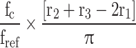
Number of switches (NSW)—Number of drivers (NDr)—Number of diodes (NDD)—Number of capacitors (NC)—Total number of structural elements (NComp)—Number of voltage sources (NDC)—Number of control signals (NCo)—Gain factor (B)—the maximum voltage stress of the switches per unit (MBVpu)—the total blocking voltage per unit (TSVpu)—the number of devices with the maximum voltage stress (NMBV)—the maximum rated voltage of the capacitors of the structure (VCmax)—the average of the conducting devices during the creation of each level (TCDav)—Cost Function (CF).
Moreover, this structure has the fewest active components per level, which leads to reduced conduction losses. The maximum voltage across the capacitors is one-third of the maximum output voltage, eliminating the need for high-voltage capacitors. In comparison Table 9, a cost function is used to evaluate the structures, which is defined by Eq. (37) [20]. According to Table 9, the cost function value in the proposed structure is lower than all the compared structures, indicating the advantage and superiority of the proposed structure over similar 13-level switched capacitor structures. Alongside the various benefits of the proposed structure compared to the other structures, this design requires four power switches with a maximum voltage equal to the peak output voltage, which limits its use for high-voltage applications. However, the proposed structure is highly suitable for lower voltage applications, such as distribution-level grid applications.
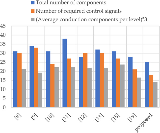
Figure 13 presents a graphical comparison between the proposed structure and recently presented similar structures based on parameters including the number of signals required for driving switches, the total number of components in the structure, and the average number of conducting semiconductors needed to produce different output voltage levels per level. According to this Figure, the proposed structure offers favorable comparison conditions.
Fig. 13.
Comparison of recent 13-level switched capacitor structures.
Also, Fig. 14 compares the proposed structure with the recent structures regarding the number of conduction devices along each of the 13 output levels. According to this Figure, the proposed structure has fewer conduction devices along the surfaces. As a result, it has a minimal value in conduction losses, especially conduction losses due to load current, compared to the recent structures. Figure 15 also compares the proposed structure with the recent structures regarding the number of state changes of separate control signals for each level change in the output voltage, according to which the proposed structure has more straightforward control and less change.
Fig. 14.

Comparison of the proposed structure with recent 13-level structures in terms of the number of Conduction devices across different levels.
Fig. 15.
Comparison of the proposed structure with recent 13-level structures in terms of the number of state changes in control signals between two levels.
Results and discussion
Simulation results
The proposed structure has been simulated using Simulink in MATLAB. The parameter values used in the simulation are listed in Table 10. The assumed values for the simulation have been kept the same as those used in the laboratory implementation to ensure that the simulation results closely match the experimental results and to allow for proper validation.
Table 10.
Parameter values.
| Parameter | Value |
|---|---|
| fref | 50 Hz |
| fSW | 2100 kHz |
| VDC | 100 V |
| Ma | 0.92 |
| C1 | 1500 uF |
| C2 | 1800 uF |
| C3 | 2200 uF |
| Ron | 0.05 Ω |
| R-L load | 200Ω ,200mH |
| R load | 160 Ω |
Figure 16 shows the simulation results for voltage, load current, and current drawn from the source over five periods of the fundamental component. According to this Figure, the output voltage has 13 voltage levels with a step of 50 V, and the maximum value is 300 V; thus, the structure’s three-fold incremental capability is characterized. In this case, with a load of 200mH + 200 , the current reaches a maximum value of 1.4 amperes, and the maximum instantaneous current drawn from the source is 19 amperes, approximately 13 times the maximum output load current. Figure 17 shows the proposed structure’s output voltage, voltage ripple, and current stress on capacitors C1 and C2. According to this Figure, capacitor C1 has a voltage of 96.5 V with a voltage ripple of 2.3%, and capacitor C2 has a voltage of 98.5 V with a ripple of 3.9%. The ripple for both capacitors is below 5% and is considered suitable. The maximum charging current for capacitor C1 is 16 amperes, while the inrush current for capacitor C2 is limited to 11 amperes by an inductor. Additionally, it is observed that in each period, the charging current for capacitor C1 spikes once, and for capacitor C2, it spikes twice. The voltage ripple for the capacitors also follows a similar trend.
Fig. 16.

Voltage and load current and input source current stress.
Fig. 17.

The output voltage, voltage ripple, and current stress of capacitors C1 and C2.
In Fig. 18, the performance of the proposed structure under dynamic load conditions is examined. Initially, the proposed structure operates under no-load conditions. At time t = 0.12 s, it is connected to a resistive-inductive load of 200mH + 200Ω, and finally, at t = 0.24 s, it is subjected to a pure resistive load of 160Ω. Figure 18 shows that the proposed structure’s 13-level output voltage is accurately generated under dynamic load conditions, and no disturbances occur in the structure’s performance. Also, in the no-load condition, the output current is zero. When switching to an RL load, the peak current increases to 1.4 amperes. Finally, under a pure resistive load of 160Ω, the load current rises to 1.9 amperes, and its waveform becomes similar to the output voltage waveform.
Fig. 18.

Voltage and current output under different loads.
Changes in voltage and load current by adjusting the dynamic modulation index are shown in Fig. 19. According to this Figure, as the modulation index increases from 0.72 to 0.92, output voltage levels rise from 11 to 13. Similarly, the load current increases from a maximum of 1.1 to 1.4 amperes. In this case, the output voltage step remains constant at 50 V. Then, as the modulation index decreases from 0.92 to 0.4, levels drop from 13 to 7. The maximum load current decreases from 1.4 to 0.6 amperes due to reduced output voltage. According to Fig. 19, the performance of the proposed structure is not disrupted by changes in the modulation index, and the voltage levels are created correctly.
Fig. 19.

Voltage and load current with dynamic changes in the modulation index.
Ripple voltage and current stress on capacitor C3 are shown in Fig. 20. The minimum and maximum voltages of capacitor C3 are 48 V and 50.1 V, respectively. As seen in the Figure, the voltage of capacitor C3 has stabilized. Based on the abovementioned values, the ripple voltage of capacitor C3 is 4.2%, which is considered acceptable. In this Figure, the current through capacitor C3 is proportional to the load current. Additionally, the voltage across this capacitor is alternately charged during one half-period and discharged during the subsequent half-period.
Fig. 20.

Voltage stress and current of capacitor C3.
Laboratory results
A laboratory prototype with an output power of 235 watts has been implemented to verify the proposed structure’s performance. Table 11 shows the specifications and components used for testing and evaluating the laboratory prototype. Additionally, Fig. 21 displays a picture of the laboratory prototype of the proposed switched capacitor 13-level inverter structure.
Table 11.
Parameters of the laboratory prototype of the proposed inverter.
| Parameter | Value |
|---|---|
| fref | 50 Hz |
| fsw | 2100 kHz |
| Vdc | 100 V |
| Ma | 0.92 |
| C1 | 1500 uF |
| C2 | 1800 uF |
| C3 | 2200 uF |
| Ron | 0.05 Ω |
| R-L load | 200 Ω,200 mH |
| R load | 160 Ω |
| Lr | 50 uH |
| Switch | FMW57N60S1HF |
| Diode | SFF200-04 |
| Driver | TLP250 |
| Controller | Arduino mega 2560 |
| Gate driver voltage | 15 V |
Fig. 21.

Picture of the laboratory prototype of the proposed structure.
Figure 22 shows the control and driving of the switches in the laboratory prototype. Since the voltage of the pulses produced by the microcontroller is 5 V, and the optimal voltage for the MOSFET gate signal is 15 V; as a result, this voltage is increased to 15 V by using an optocoupler, and finally, the necessary amount is provided for the activation of the switch gate signal.
Fig. 22.

Control schematic of TLP250 driver.
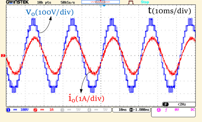
Figure 23 shows the voltage across the resistive-inductive load and its current for five periods of the fundamental component. According to this Figure, the 13 output voltage levels with a step of 50 V and a maximum output voltage three times the input, i.e., 300 V, are correctly generated. With a load of 200mH + 200 the output current also reaches a peak of 1.4 amperes.
Fig. 23.
Voltage and current across the output load with resistive-inductive load.
Figure 24 examines the correctness of the structure’s performance under dynamic changes in the output load. With a resistive load of 160 , the load current reaches a maximum value of 1.9 amperes, and the current waveform resembles the output voltage waveform. With the dynamic change from a resistive load to an inductive-resistive load of 200mH + 200
 , the maximum load current decreases to 1.4 amperes. The structure generates 13 output levels successfully, and the load current becomes more sinusoidal.
Fig. 24.

Output voltage and current with load change from resistive to resistive-inductive.
Figure 25 shows different capacitors’ input and charging currents over 2.5 primary cycles. As shown in Fig. 25a, the charging current of capacitor C1, in the normal state and without a limiting inductor, is not excessively high due to this capacitor’s capability and proper charging sequence. In Fig. 25b, with an inductor limiter in the capacitor C2 loop, its charging current is limited and reaches a maximum of 11 amperes. The charging current of capacitor C3, which is in series with switch Sc, is shown in Fig. 25c and is similar to the load current. Due to the load impedance in the charging path of capacitor C3, this capacitor does not experience significant current stress, and the output load current passes through it.
Fig. 25.

Charging current stress of capacitors; (a) Current stress on capacitor C1, (b) Current stress on capacitor C2, (c) Current stress on capacitor C3.
The voltage of the capacitors in the proposed structure is shown in Fig. 26. In Fig. 26a, the average voltage of the capacitors is shown, with the values for capacitors C1, C2, and C3 being 100, 100, and 50 V, respectively. Figure 26b displays the ripple voltage of the capacitors in the proposed structure. The voltage ripple of capacitor C1 is 2.3 V, which is 2.3%; the ripple voltage of capacitor C2 is 3.7 V, equivalent to 3.7%, and finally, the ripple voltage of capacitor C3 is 1.9 V and is equal to 3.8%. According to the results in this Figure, the voltage ripple for all three capacitors is within the acceptable range, less than 5%.
Fig. 26.

Voltage of the capacitors in the proposed structure: (a) Average capacitor voltage, (b) Voltage ripple of the capacitors.
Figure 27 analyzes the voltage across the proposed structure’s power switches. According to this Figure, the maximum voltage stress in four power switches is equal to 300 V; in three power switches, it is equal to 200 V; in two switches, it is equal to 100 V; and finally, in two power switches it is equal to 50 V. In addition, the switching frequency of the power switches is also observable in this Figure. Switches Sc and Sʹc experience continuous stress from frequent switching on and off compared to the other power switches; however, the other switches do not undergo significant stress in constant switching.
Fig. 27.

Voltage stress of the components in the proposed structure.
Conclusion
In this paper, a single-source switched capacitor 13-level inverter with a three-fold voltage gain has been presented. This converter can maintain capacitor voltage balance throughout the positive and negative half-period of the output voltage. The proposed structure has fewer components than 13-level inverters and requires fewer switch control signals without high-voltage capacitors. Based on recent studies, a comparative evaluation of the proposed structure shows that its advantages and cost function are lower than those of similar structures. Reducing current conductor components per level indicates lower conduction losses in the proposed structure. Also, when transitioning from one level to the next, the proposed structure requires fewer state-changing signals, which results in more straightforward control and reduced switching losses. The balance of capacitor voltages, the details of their values, and the various losses present in the proposed inverter have been thoroughly examined. A small limiting inductance is used in series with the capacitor and the components within its charging path to decrease the magnitude of the inrush current. Finally, the modulation strategy and performance of the proposed structure were evaluated and simulated in the Matlab/Simulink environment. Experimental results for the proposed inverter have also been provided. The obtained results demonstrate the high quality of the output waveforms of the proposed converter, confirming both theoretical and simulation analyses for both steady and dynamic states.
Author contributions
All authors reviewed the manuscript. H. M. designed and performed all the experiments, data analysis, and documentation. M. H. designed and performed the experiment, data analysis, and documentation. A. S. designed as well as participated in the experimental design and tests. M. S. performed the data analysis and supervision.
Data availability
All data generated and analysed during the current study are available from the corresponding author on reasonable request.
Declarations
Competing interests
The authors declare no competing interests.
Footnotes
Publisher’s note
Springer Nature remains neutral with regard to jurisdictional claims in published maps and institutional affiliations.
References
- 1.Siddique, M. D., Mekhilef, S., Shah, N. M., Ali, J. S. M. & Blaabjerg, F. A new switched capacitor 7L inverter with triple voltage gain and low voltage stress. IEEE Trans. Circuits Syst. II Express Briefs67(7), 1294–1298 (2020). [Google Scholar]
- 2.Bhatnagar, P., Singh, A. K., Gupta, K. K. & Siwakoti, Y. P. A switched-capacitors-based 13-level inverter. IEEE Trans. Power Electron.37(1), 644–658 (2022). [Google Scholar]
- 3.Goel, R., Davis, T. T. & Dey, A. Thirteen-level multilevel inverter structure having single DC source and reduced device count. IEEE Trans. Ind. Appl.58(4), 4932–4942 (2023). [Google Scholar]
- 4.Sheng, W. & Ge, Q. A novel seven-level ANPC converter topology and its commutating strategies. IEEE Trans. Power Electron.33(9), 7496–7509 (2017). [Google Scholar]
- 5.Lee, S. S., Lim, C. S. & Lee, K. B. Novel active-neutral-point-clamped inverters with improved voltage-boosting capability. IEEE Trans. Power Electron.35(6), 5978–5986 (2019). [Google Scholar]
- 6.Liu, J., Wu, J., Zeng, J. & Guo, H. A novel nine-level inverter employing one voltage source and reduced components as high-frequency AC power source. IEEE Trans. Power Electron.32(4), 2939–2947 (2016). [Google Scholar]
- 7.Lee, S. S. Single-stage switched-capacitor module (S 3 CM) topology for cascaded multilevel inverter. IEEE Trans. Power Electron.33(10), 8204–8207 (2018). [Google Scholar]
- 8.Panda, K. P., Bana, P. R. & Panda, G. A reduced device count single DC hybrid switched-capacitor self-balanced inverter. IEEE Trans. Circuits Syst. II Express Briefs68(3), 978–982 (2020). [Google Scholar]
- 9.Roy, T. & Sadhu, P. K. A step-up multilevel inverter topology using novel switched capacitor converters with reduced components. IEEE Trans. Industr. Electron.68(1), 236–247 (2020). [Google Scholar]
- 10.Ye, Y., Zhang, G., Wang, X., Yi, Y. & Cheng, K. W. E. Self-balanced switched-capacitor thirteen-level inverters with reduced capacitors count. IEEE Trans. Industr. Electron.69(1), 1070–1076 (2021). [Google Scholar]
- 11.Roy, T., Sadhu, P. K. & Dasgupta, A. Cross-switched multilevel inverter using novel switched capacitor converters. IEEE Trans. Industr. Electron.66(11), 8521–8532 (2019). [Google Scholar]
- 12.Bhatnagar, P., Singh, A. K., Gupta, K. K. & Siwakoti, Y. P. A switched-capacitors-based 13-level inverter. IEEE Trans. Power Electron.37(1), 644–658 (2021). [Google Scholar]
- 13.Islam, S., Siddique, M. D., Iqbal, A. & Mekhilef, S. A 9-and 13-level switched-capacitor-based multilevel inverter with enhanced self-balanced capacitor voltage capability. IEEE J. Emerging Select. Topics Power Electron.10(6), 7225–7237 (2022). [Google Scholar]
- 14.Barzegarkhoo, R., Forouzesh, M., Lee, S. S., Blaabjerg, F. & Siwakoti, Y. P. Switched-capacitor multilevel inverters: A comprehensive review. IEEE Trans. Power Electron.37(9), 11209–11243 (2022). [Google Scholar]
- 15.Singh, A. K. & Mandal, R. K. A novel 17-level reduced component single DC switched-capacitor-based inverter with reduced input spike current. IEEE J. Emerging Selected Topics Power Electron.10(5), 6045–6056 (2022). [Google Scholar]
- 16.Sandeep, N. A 13-level switched-capacitor-based boosting inverter. IEEE Trans. Circuits Syst. II Express Briefs68(3), 998–1002 (2020). [Google Scholar]
- 17.Foti, S., Scimone, T., Oteri, A., Scelba, G. & Testa, A. A reduced switch count, self-balanced, 13-level inverter based on a dual T-type configuration. IEEE Trans. Power Electron.38(9), 11010–11022 (2023). [Google Scholar]
- 18.Peddapati, S. & Kumar, B. A voltage-boosting seven-level switched capacitor multilevel inverter with reduced device count. IEEE J. Emerging Select. Topics12(1), 743–753 (2024). [Google Scholar]
Associated Data
This section collects any data citations, data availability statements, or supplementary materials included in this article.
Data Availability Statement
All data generated and analysed during the current study are available from the corresponding author on reasonable request.