Abstract
Vanadium dioxide (VO2) exhibits exceptional phase transition characteristics that enable dynamic manipulation of electromagnetic wave. In this study, a novel design of bilayer isotropic metasurface is introduced. It leverages insulating-to-metallic phase transition of VO2 to enable broadband holography for terahertz wave. For the metallic VO2, the upper VO2 antennas reflect incident terahertz wave and generate hologram. For the insulating VO2, incident wave is reflected by the lower gold antennas and the same hologram is generated with frequency doubling. Working frequencies of the designed holograms are 1.2 THz for metallic VO2 and 1.9 THz for insulating VO2. Due to the broadband performance under each state, the proposed metasurface can achieve holography within 1.0-2.1 THz. It is noteworthy that the generated holograms under two states of VO2 remain entirely independent, and another metasurface that achieves frequency-multiplexed holograms is presented. Our design may have possible applications in holographic display and information encryption.
Keywords: Metasurface, Hologram, Terahertz, VO2
Subject terms: Nanophotonics and plasmonics, Metamaterials
Introduction
Electromagnetic (EM) waves are widely employed across numerous scientific fields, serving as our pivotal tools for comprehending and harnessing intricacies of the world. Within EM spectrum, terahertz waves occupy a distinctive position, delineated by wavelengths spanning from 3000 to 30 micrometers, which fall between microwave and infrared radiation. Nonetheless, people’s comprehension of terahertz waves has historically lagged that of microwave and infrared technologies due to their idiosyncratic attributes. Yet, the 21st century has witnessed a burgeoning recognition of the significance of terahertz waves1–3. Meanwhile, terahertz waves have shown enormous potential in fields such as biomedicine4,5 and wireless communication6,7. Terahertz waves exhibit an expanded broadband capacity and heightened spectrum utilization, thus emerging as a pivotal technology underpinning the evolution of sixth generation wireless systems8,9. However, the burgeoning complexity of application scenarios underscores an imperative for terahertz devices to embody attributes of diminutive size, multifaceted channel support, and broadband capability. This necessitates a paradigm shift towards the development of compact, multi-channel, and broadband-enabled terahertz devices to effectively navigate the exigencies of contemporary application landscapes.
In recent years, the limitations posed by the intrinsic complexity of natural materials have spurred interest in alternative approaches for precise control over terahertz waves. Metamaterials have emerged as a prominent artificial counterpart, garnering considerable attention owing to their exceptional EM properties. Through the deliberate design of specialized element arrays, metamaterials manifest unique EM responses, including but not limited to, negative refractive index phenomena10. However, due to its high loss and difficulty in production, metasurface as two-dimensional counterpart has become the preferred choice for people. In comparison to metamaterial counterparts, metasurfaces offer a compelling alternative, characterized by simplified structure, diminished loss, and enhanced cost-effectiveness. These attributes have significantly broadened the scope of their application domains. Metasurfaces wield the capacity to flexibly modulate various EM attributes such as polarization, amplitude, and phase11–13. This flexibility stems from the optimization of geometric parameters of the constituent meta-atoms. Through meticulous engineering, metasurfaces have achieved a myriad of functionalities including planar focusing14–17, vortex beam18,19, and broadband absorption20,21. Moreover, the augmentation of degrees of freedom has facilitated multi-channel reuse, thereby promoting the realization of multifunctional integration and enabling advanced applications such as information encryption22. In essence, metasurfaces epitomize a paradigm shift in EM manipulation, affording the unprecedented versatility and efficacy across diverse application landscapes.
Achievements of metasurfaces in holography are remarkable. Holography, by measuring amplitude as well as phase characteristics of wave, enables the presentation of three-dimensional images, thereby yielding more authentic and visually immersive effects. In contrast to conventional imaging techniques, holography boasts a richer detail. Holography requires high clarity and resolution, and metasurfaces are capable of precisely adjusting amplitude as well as phase of EM waves. Therefore, metasurface holography has high application value. In recent years, this technology has made many breakthroughs. In 2013, Ni et al. introduced a novel structural paradigm to effectively generate holograms under visible light incidences, thus demonstrating a practical avenue for complex hologram production utilizing metasurfaces23. In 2015, Zheng et al. devised a geometric metasurface that substantially augmented diffraction efficiency of holograms engendered by circularly polarized incident light to an impressive 80%24. Concurrently, Wen et al. pioneered the integration of multiplexing concepts into holography, thereby enhancing the information capacity of metasurface25. Arbabi et al. refined the design methodologies pertaining to transmissive metasurfaces, thereby bolstering their efficacy in polarization and phase control26. In 2016, Liu et al. delved into the realm of anisotropic metasurfaces, unveiling their robust proficiency in manipulating terahertz waves27. Wang et al. presented a dielectric metasurface constructed from silicon nano-blocks, facilitating the simultaneous wavefront manipulation of three primary color lights28. In 2021, Bao et al. presented a strategy that breaks the traditional constraint of four degrees of freedom, resulting in a six-degree-of-freedom metasurface with the impressive performance in metasurface holography29. So far, there are still many breakthroughs in metasurface holography, which is one of the hot research areas related to metasurfaces.
Generally, once a metasurface sample is fabricated, it is challenging to alter its internal structural parameters. However, if methods can be developed to allow changes in physical properties of metasurface, its range of potential applications would be significantly broadened. Currently, the dynamic metasurface represents a frontier approach to achieving this goal30,31. Dynamic metasurface can modulate electromagnetic response through mechanisms such as electrical control32. The incorporation of phase-change materials (PCMs) is a promising method for realizing dynamic metasurfaces. PCMs are those that alter their state in response to external conditions without changing their fundamental structure. These materials exhibit distinct physical properties in different states, which is advantageous for multifunctional integration. Since the inception of metasurface research, many PCMs have been successfully applied to metasurfaces, including liquid crystal33, doped semiconductor34, GeSbTe35, and graphene36. Among numerous materials, VO2 stands out as a prominent PCM due to simple phase-change conditions and excellent performances. VO2 is capable of reversible switching between metallic and insulating states. At room temperature, VO2 exhibits insulating properties, whereas it behaves as a metal as temperature rises above 68 °C. Electrical conductivity of VO2 differs by three orders of magnitude between two states, leading to significant changes in properties such as optical and electrical characteristics. Moreover, the transition of VO2 states can be induced by electrical or light stimulation37,38. Extensive research has been conducted to harness unique properties of VO2. In 2018, Ding et al. presented a broadband metasurface using VO2, allowing it to switch from an absorber to a reflecting half-wave plate39. Two years later, Zhang et al. designed a multifunctional metasurface by using properties of VO2, which enabled polarization state conversion and wide-range absorption40. Building upon this foundation, Liu and colleagues simultaneously utilized graphene and VO2 to design a composite-configured dual-tunable absorption modulator41. These applications demonstrate the potential of PCMs like VO2 and pave the way for new applications in dynamic modulation and tunable functional devices.
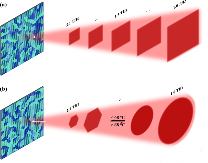
This study presents the design of VO2 metasurfaces to achieve broadband holography for terahertz wave. The proposed metasurfaces can achieve holography within 1.0-2.1 THz. By exploiting the capacity to switch dielectric condition of VO2, EM waves are redirected to different positions within the bilayer structure, enabling to generate holograms across distinct frequency bands. Notably, holograms produced in two states of VO2 are found to be independent. Through careful alignment of center frequencies of imaging bands in both states, the metasurface demonstrates the capability for broadband holography. To optimize performance, four meta-atoms with phase difference of 90° are meticulously designed for each VO2 state, ensuring comprehensive phase coverage and thereby enhancing the clarity and resolution of the resultant holograms. To elucidate operational principles of the designed metasurfaces, functional diagrams are provided in Fig. 1. In Fig. 1a, a square broadband hologram is designed with the center frequency of the imaging band at 1.2 THz for the metallic VO2 and 1.9 THz for the insulating VO2. Successful generation of broadband holograms at 1.0-2.1 THz is achieved. To illustrate the impact of VO2 state switching and the independence of upper- and lower-layer images, a secondary sample is devised in Fig. 1b. This sample features a circular hologram for the metallic VO2 and a hexagonal hologram for the insulating VO2. Variation in temperature leads to corresponding alterations in the resulting holograms, further confirming the versatility and functionality of the proposed metasurface design.
Fig. 1.
Schematic diagrams of the designed metasurfaces, which achieves holography within 1.0-2.1 THz. (a) A square broadband hologram achieved by designing the same image for two states of VO2. (b) Broadband holograms achieved by designing different images for two different states of VO2.
Principle and design
The meta-atom is made of a bilayer structure. Each layer consists of three components including a designed antenna positioned in the upper section, a dielectric spacer in the middle, and a metallic substrate located in the lower section. This structure can form a metal-insulator-metal (MIM) space. Terahertz waves are capable of strongly engaging with MIM structure and being controlled by the specially designed antenna. VO2 possesses excellent phase transition capabilities, allowing for the modulation of its conductivity by controlling temperature. Generally, at temperatures below 68 °C, VO2 exhibits a conductivity of approximately 200 S/m, signaling an insulating state. In contrast, at temperatures above 68 °C, VO2 exhibits a conductivity of approximately  S/m, signaling a metallic state. Working state of the upper MIM cavity is controlled by VO2, enhancing control capabilities of meta-atoms over terahertz waves. For the metallic VO2, substrate of the upper MIM structure can be approximated as metal substrate, thereby preventing transmission of incident wave and allowing only the upper MIM structure to function. Conversely, for the insulating VO2, the influence of the upper MIM structure on incident wave can be neglected, effectively making only the lower MIM structure operational.
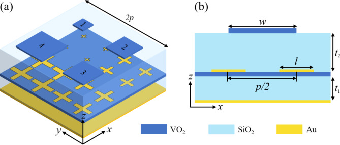
Figure 2 illustrates the proposed meta-atoms. Figure 2a presents a three-dimensional view of a localized meta-atom array, showcasing structural parameters utilized for achieving broadband terahertz holography. Period of p = 100.0 μm is used for meta-atom. The proposed meta-atom consists of two MIM structures. For the upper MIM, the antenna is square-shaped, and both the antenna and the substrate are composed of VO2. For the lower MIM, the antenna is cross-shaped, and both the antenna and the substrate are gold. The advantage of this isotropic bilayer structure lies in its ability to nearly eliminate cross polarization and coupling effect between each layer. The dielectric material for both MIM spacers is silicon dioxide (SiO2). The thickness of VO2 layers is tv = 1.0 μm, while that of gold layers is tg = 0.5 μm. The thickness of the upper SiO2 spacer is t2 = 19.0 μm, and that of the lower SiO2 spacer is t1 = 10.0 μm. These parameters are presented in Fig. 2b.
Fig. 2.
(a) A three-dimensional view of a  array of meta-atoms, showcasing antenna parameters for two sets of antennas within two MIM cavities. The square VO2 antennas have widths of w1 = 12.0 μm, w2 = 45.5 μm, w3 = 51.6 μm, and w4 = 74.0 μm, while dimensions of the cross-shaped gold antenna with an aspect ratio of 5:1 are given as l1 = 5.0 μm, l2 = 29.8 μm, l3 = 34.6 μm, and l4 = 45.0 μm. (b) The side view of the designed meta-atom, which is segmented into six components in two MIM structures.
Within this bilayer structure, gold antenna is embedded in the dielectric spacer of upper MIM structure, and it is distributed centrally in square regions with the period of p/2. Gold antenna is isotropic with a length-to-width ratio of 5:1. Through simulation, four meta-atoms are achieved, and each exhibits a 90° phase difference as VO2 is insulator. Four values of the length of gold antenna are l1 = 5.0 μm, l2 = 29.8 μm, l3 = 34.6 μm, and l4 = 45.0 μm. The upper VO2 square antenna is positioned at the center of each meta-atom. Similarly, for the metallic VO2, four meta-atoms are achieved and each exhibits a 90° phase difference. As illustrated in Fig. 2a, four values of the width of VO2 square antenna are w1 = 12.0 μm, w2 = 45.5 μm, w3 = 51.6 μm, and w4 = 74.0 μm. Dielectric constant of SiO2 is 3.85. Gold is a lossy metal with a conductivity of  S/m. Drude model is commonly used to describe dielectric constant of VO2. Drude model is
  , where
  ,
,  with
with  ,
,  , and
, and  42–44. In simulation, the conductivity of VO2 is
  as it is metallic (insulating).
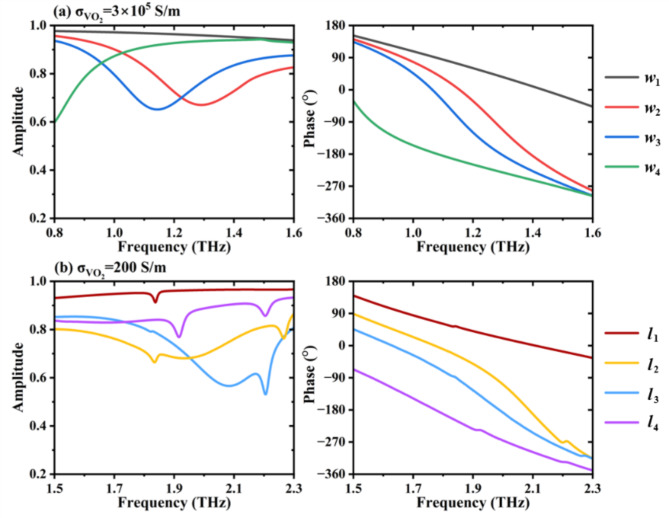
To achieve clear holograms, the proposed meta-atoms should exhibit 270° phase coverage with high reflectivity. Additionally, to enhance imaging efficiency, the number of meta-atom type should be kept to a minimum. Finite element method is employed in this study. Meta-atoms are arranged with periodic boundary conditions in x and y directions. Figure 3 illustrates simulation results of amplitudes and phases of meta-atoms under two states of VO2. For the metallic VO2 with w1 = 12.0 μm, w2 = 45.5 μm, w3 = 51.6 μm, and w4 = 74.0 μm as four suitable parameters, the desired effects are achieved by varying the width of the upper square VO2 antennas. Conversely, for the insulating VO2 with l1 = 5.0 μm, l2 = 29.8 μm, l3 = 34.6 μm, and l4 = 45.0 μm as four suitable parameters, the desired effects are attained by altering length and width of gold crosses. As depicted in Fig. 3a, amplitudes with four parameters are above 0.65 within 1.0-1.4 THz, and phase coverage with four parameters approximately meets 270°. We choose 1.2 THz as the center frequency for broadband imaging when VO2 is metallic. In Fig. 3b, amplitudes are above 0.68 within 1.4–2.1 THz, and 90° phase difference is achieved between each meta-atom, indicating a broader bandwidth for achieving high-definition holography. We choose 1.9 THz as the center frequency for broadband imaging when VO2 is insulating. Roles of two sets of parameters are independent of each other. For the metallic VO2, the choice of the length of gold antenna doesn’t affect characteristics of meta-atoms, while for the insulating VO2, the choice of the width of VO2 antenna is similarly inconsequential. It is worth mentioning that there is still room for optimization. Uniform quality of broadband holography is realized based on the 90o discrete phase coverage of meta-atoms. The different phase response in the frequency band should be optimized to be more parallel for better broadband performance. Optimization algorithm such as gradient descent method could be further used.
Fig. 3.
Simulation results of basic characteristics of the designed meta-atoms for two states of VO2. (a) For the metallic VO2, simulated basic responses of the designed meta-atoms. (b) For the insulating VO2, simulated basic responses of the designed meta-atoms.
Results and discussion
The key to the design of metasurface hologram lies in determining phase distribution of the metasurface. This design process, known as phase retrieval, obtains corresponding phase distribution from a known amplitude distribution of image. This work adopts Gerchberg-Saxton (GS) algorithm for phase retrieval due to its suitability for computational technique, avoiding the need for complex setups and thus rendering phase search process highly efficient and accurate.
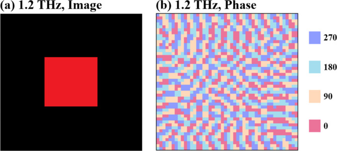
Based on GS algorithm, we design a terahertz metasurface comprising 46 × 46 meta-atoms for generating broadband holograms. Far-field monitors are placed with 0.1 THz interval at 1.0-2.1 THz. Image of the desired hologram in far field at 1.2 THz is illustrated in Fig. 4a. Based on this image, phase distribution of metasurface is obtained after iterations of GS algorithm in Fig. 4b. Within 1.0-1.4 THz, VO2 is metal. When incident wave travels, only upper MIM structure is active for each meta-atom. This is because VO2 substrate of upper MIM structure reflects the most part of incident wave, thereby preventing it from interacting with lower MIM structure. At this point, basic characteristics of metasurface are influenced by upper VO2 antenna. Four designed square VO2 antennas yield four different phase responses of reflected wave, serving as basic elements for phase distribution of the designed metasurface as VO2 is metallic in Fig. 4b. Within 1.5–2.1 THz, VO2 is insulator. At this stage, VO2 structures in upper MIM do not reflect incident wave. Incident wave transmits through upper MIM, leaving only lower MIM structure active. At this point, basic characteristics of metasurface depend on lower cross-shaped gold antenna. Four designed cross-shaped gold antennas yield four different phase responses of reflected wave, serving as basic elements for phase distribution of the designed metasurface as VO2 is insulating in Fig. 4b.
Fig. 4.
(a) The ideal amplitude of far-field hologram at 1.2 THz. (b) The ideal phase distribution of the metasurface at 1.2 THz.
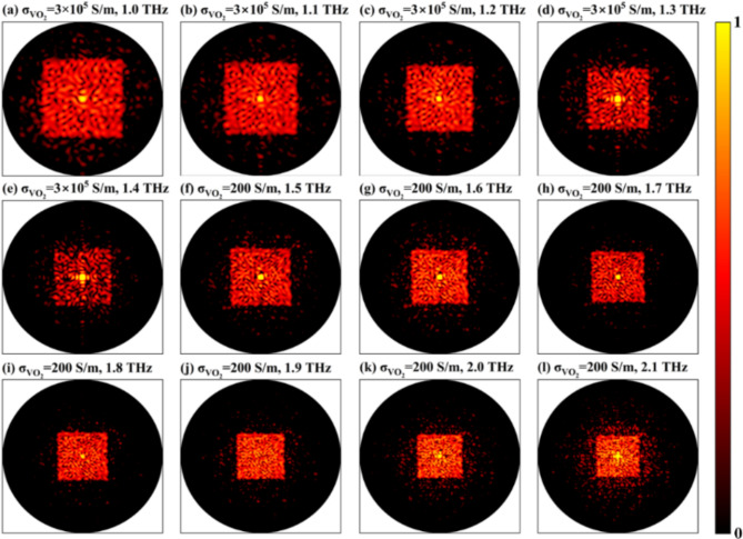
Simulated holograms are presented with the normalized intensity in Fig. 5. Figure 5a–e correspond to simulated results as VO2 is metallic, while Fig. 5f–k correspond to simulated results as VO2 is insulating. Imaging quality is optimized at center frequencies of 1.2 THz and 1.9 THz for these two frequency bands. Evaluation of hologram efficiency is carried out by calculating the far-field power ratio between the proposed metasurface and a metal mirror. At 1.2 THz, hologram efficiency is 55.6%. Compared with the original image, root mean square error (RMSE) represents the quantified fidelity of hologram. Calculated RMSE for hologram is 0.058 at 1.2 THz, and it indicates higher fidelity. Holograms at other frequencies also exhibit sufficient clarity and integrity. However, the quality of holograms at 1.4 THz and 2.1 THz is somewhat inferior compared to others. It aligns with results in Fig. 3. Despite this, the produced holograms are relatively acceptable.
Fig. 5.
The simulated holograms within 1.0-2.1 THz. (a–e) The obtained holograms as VO2 are metallic. (f–l) The obtained holograms as VO2 are insulating.
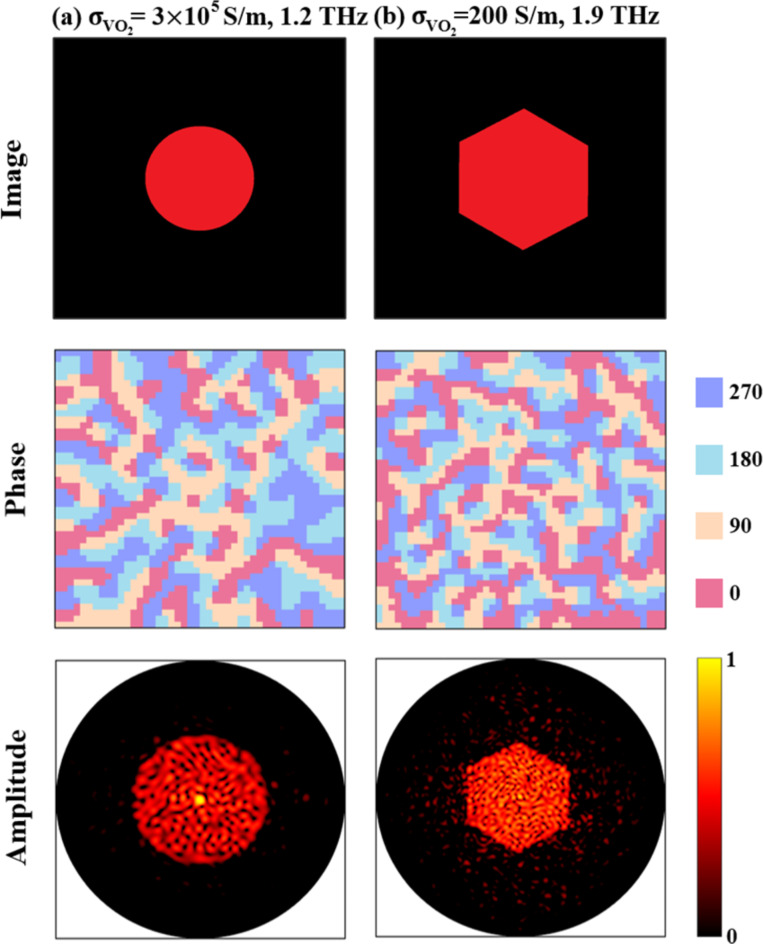
Our work also presents another metasurface to generate frequency-multiplexed broadband hologram, demonstrating the independence of two broadband terahertz holograms. In simulation, this metasurface comprises 46 × 46 meta-atoms, and simulation method and setup of far-field monitors are consistent with those used for the previous metasurface. In contrast to the previous case, holograms generated by this metasurface are circular when VO2 is metallic, while those generated are hexagonal when VO2 is insulating. We present images of holograms at center frequencies for both states of VO2 in Fig. 6. Design method of hologram remains the same as that of the previous metasurface. We arrange square VO2 antennas of upper MIM according to phase distribution in Fig. 6a and cross-shaped gold antennas of lower MIM according to phase distribution in Fig. 6b. This allows us to obtain two independent sets of holograms within 1.0-2.1 THz, which are solely controlled by the state of VO2. Obtained holograms at 1.2 THz and 1.9 THz are displayed in Fig. 6. It is seen that the quality of both holograms is acceptable. Simulated hologram efficiencies are 55.7% and 85.9% for these two center frequencies, indicating the efficient performance. Compared with their original images, RMSEs are calculated as 0.053 and 0.052.
Fig. 6.
(a) The ideal amplitude of far-field hologram, phase distribution of the metasurface, and actual amplitude of the circular hologram as VO2 is metallic at 1.2 THz. (b) The ideal amplitude of far-field hologram, phase distribution of the metasurface, and actual amplitude of the hexagonal hologram as VO2 is insulating at 1.9 THz.
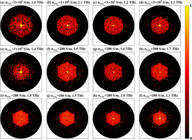
Furthermore, Fig. 7 shows obtained broadband holograms within 1.0-2.1 THz. Figure 7a–e represent simulated results when VO2 is metallic, and Fig. 7f–k represent simulated results when VO2 is insulating. It is evident that high-resolution holograms are produced within 1.0-2.1 THz even when image is altered. By varying the state of VO2, it is possible to switch images across different frequency bands, thereby achieving frequency-multiplexed broadband holograms. This demonstrates the independence of the proposed broadband holograms.
Fig. 7.
Broadband terahertz frequency-multiplexed holograms. (a–e) The obtained circular holograms as VO2 are metallic. (f–l) The obtained hexagonal holograms as VO2 are insulating.
Potential sample manufacturing and experimental measurement
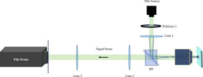
The possible sample manufacturing steps for our designs mainly include lithography and deposition techniques. The lateral view of a single meta-atom in Fig. 8 provides a detailed representation of manufacturing process. Beginning with a SiO2 substrate, a gold substrate and a SiO2 spacer are deposited one after another. Subsequently, a VO2 film is sputtered onto the structure and annealed. Next, a layer of photoresist is spin-coated onto the surface and patterned using optical lithography to define the shape of cross-like patches for the lower MIM structure. A gold layer is then deposited over the patterned photoresist using electron beam evaporation. The lift-off process is employed to dissolve the photoresist, removing the excess gold and leaving behind the desired patterned gold patches. Then, another SiO2 layer is deposited via electron beam evaporation. A second layer of photoresist is applied and shaped using optical lithography to define the square-shaped patches for the upper MIM structure. VO2 is sputtered over the patterned photoresist, and another lift-off process is used to remove the photoresist and the extra VO2 layer, leaving the final VO2 patches. These remaining patches are then annealed to achieve the fabrication of the metasurface. Potential hologram measurement system is shown in Fig. 9. The entire system consists of a source, three lenses, an objective lens, a beam splitter, a linear polarizer, and a detector. In the measurement of far-field hologram, terahertz wave is emitted from the terahertz source and polarized by a linear polarizer. The rear plane of lens 1 and the objective lens are confocal, so that terahertz wave can be normally incident on the sample. The reflected signal is collected by the terahertz detector through confocal lenses 2 and 3, thus realizing the detection of hologram in the far field.
Fig. 8.
Potential fabrication process of the proposed VO2 metasurface.
Fig. 9.
Potential hologram measurement system.
Conclusion
Utilizing a bilayer MIM structure based on VO2, this work presents a novel approach for achieving broadband terahertz holography. For the metallic VO2, the upper VO2 square antennas reflect EM wave, yielding broadband holograms centered at 1.2 THz. Conversely, for the insulating VO2, the lower gold cross-shaped antennas reflect terahertz wave, generating broadband holograms centered at 1.9 THz. Two frequency bands are closely adjacent by controlling the state transition of VO2, allowing for the creation of broadband holograms within 1.0-2.1 THz. Furthermore, by altering the pattern of the hologram, the independence and adjustability of hologram are demonstrated under two states of VO2. Compared to existing terahertz holography methods45–48, our scheme has the limited channel number. However, our design offers higher holographic efficiency, polarization-insensitive control, and a broader bandwidth. There is potential for our designed VO2 metasurface to be used in wavefront engineering49 and holographic encryption50.
Author contributions
Jiayu Zhao, Runxuan Zhang, Sicheng Cao, Mingwei Zhuang, and Zhengyong Song: Data curation, Investigation, Writing - original draft. Mingwei Zhuang and Zhengyong Song: Conceptualization, Funding acquisition, Supervision, Writing - review & editing.
Funding
This work is supported by Fujian Provincial Natural Science Foundation of China (2024J01053) and Natural Science Foundation of Xiamen (3502Z202473013).
Data availability
The datasets used and/or analysed during the current study available from the corresponding author on reasonable request.
Declarations
Competing interests
The authors declare no competing interests.
Footnotes
Publisher’s note
Springer Nature remains neutral with regard to jurisdictional claims in published maps and institutional affiliations.
Contributor Information
Mingwei Zhuang, Email: mw.zhuang@xmu.edu.cn.
Zhengyong Song, Email: zhysong@xmu.edu.cn.
References
- 1.Grady, N. K. et al. Terahertz metamaterials for linear polarization conversion and anomalous refraction. Science340(6138), 1304–1307 (2013). [DOI] [PubMed] [Google Scholar]
- 2.Zhang, X. Q. et al. Terahertz surface plasmonic waves: A review. Adv. Photonics. 2(1), 014001 (2020). [Google Scholar]
- 3.Liu, M., Yang, J., Du, Z., Xin, J. & Song, Z. Tripolarization-channel holograms generated by terahertz reflective bilayer-metasurface. Opt. Lasers Eng.186, 108763 (2025). [Google Scholar]
- 4.Ahmadivand, A., Gerislioglu, B., Ahuja, R. & Mishra, Y. K. Terahertz plasmonics: the rise of toroidal metadevices towards immunobiosensings. Mater. Today32, 108–130 (2020). [Google Scholar]
- 5.Yang, X. et al. Biomedical applications of terahertz spectroscopy and imaging. Trends Biotechnol.34(10), 810–824 (2016). [DOI] [PubMed] [Google Scholar]
- 6.Huang, Y., Shen, Y. C. & Wang, J. Y. From terahertz imaging to terahertz wireless communications. Engineering22, 106–124 (2023). [Google Scholar]
- 7.Ma, J. J. et al. Security and eavesdropping in terahertz wireless links. Nature563(7729), 89–93 (2018). [DOI] [PubMed] [Google Scholar]
- 8.Kildishev, A. V., Boltasseva, A. & Shalaev, V. M. Planar photonics with metasurfaces. Science339(6125), 1232009 (2013). [DOI] [PubMed] [Google Scholar]
- 9.Leonhardt, U. Optical conformal mapping. Science312(5781), 1777–1780 (2006). [DOI] [PubMed] [Google Scholar]
- 10.Smith, D. R., Pendry, J. B. & Wiltshire, M. C. K. Metamaterials and negative refractive index. Science305(5685), 788–792 (2004). [DOI] [PubMed] [Google Scholar]
- 11.Yu, N. F. et al. Light propagation with phase discontinuities: Generalized laws of reflection and refraction. Science334(6054), 333–337 (2011). [DOI] [PubMed] [Google Scholar]
- 12.Xu, Z., Yang, J. & Song, Z. Terahertz switchable metasurface for polarization conversion and hologram manipulation. Opt. Lasers Eng.184, 108641 (2025). [Google Scholar]
- 13.Yang, J., Xu, Z., Xin, J. & Song, Z. Temperature-assisted terahertz reconfigurable metasurface for multi-polarization holographic display and encryption. Opt. Laser Technol.181, 111968 (2025). [Google Scholar]
- 14.Wang, S. M. et al. A broadband achromatic metalens in the visible. Nat. Nanotechnol13(3), 227–232 (2018). [DOI] [PubMed] [Google Scholar]
- 15.Avayu, O., Almeida, E., Prior, Y. & Ellenbogen, T. Composite functional metasurfaces for multispectral achromatic optics. Nat. Commun.8, 14992 (2017). [DOI] [PMC free article] [PubMed] [Google Scholar]
- 16.Chen, W. T., Zhu, A. Y., Sisler, J., Bharwani, Z. & Capasso, F. A broadband achromatic polarization-insensitive metalens consisting of anisotropic nanostructures. Nat. Commun.10, 355 (2019). [DOI] [PMC free article] [PubMed] [Google Scholar]
- 17.Arbabi, E. et al. MEMS-tunable dielectric metasurface lens. Nat. Commun.9, 812 (2018). [DOI] [PMC free article] [PubMed] [Google Scholar]
- 18.Devlin, R. C., Ambrosio, A., Rubin, N. A., Mueller, J. P. B. & Capasso, F. Arbitrary spin-to-orbital angular momentum conversion of light. Science358(6365), 896–900 (2017). [DOI] [PubMed] [Google Scholar]
- 19.Guo, K., Xin, J. & Song, Z. Terahertz six-channel metasurface for the dynamic modulation of OAM. J. Phys. D Appl. Phys.58(6), 065109 (2025). [Google Scholar]
- 20.Kenney, M. et al. Octave-spanning broadband absorption of terahertz light using metasurface fractal-cross absorbers. ACS Photonics4(10), 2604–2612 (2017). [Google Scholar]
- 21.Aydin, K., Ferry, V. E., Briggs, R. M. & Atwater, H. A. Broadband polarization-independent resonant light absorption using ultrathin plasmonic super absorbers. Nat. Commun.2, 517 (2011). [DOI] [PubMed] [Google Scholar]
- 22.Zheng, P. X. et al. Metasurface-based key for computational imaging encryption. Sci. Adv.7(21), eabg0363 (2021). [DOI] [PMC free article] [PubMed] [Google Scholar]
- 23.Ni, X. J., Kildishev, A. V. & Shalaev, V. M. Metasurface holograms for visible light. Nat. Commun.4, 2807 (2013). [Google Scholar]
- 24.Zheng, G. X. et al. Metasurface holograms reaching 80% efficiency. Nat. Nanotechnol. 10(4), 308–312 (2015). [DOI] [PubMed] [Google Scholar]
- 25.Wen, D. D. et al. Helicity multiplexed broadband metasurface holograms. Nat. Commun.6, 8241 (2015). [DOI] [PMC free article] [PubMed] [Google Scholar]
- 26.Arbabi, A., Horie, Y., Bagheri, M. & Faraon, A. Dielectric metasurfaces for complete control of phase and polarization with subwavelength spatial resolution and high transmission. Nat. Nanotechnol. 10(11), 937–943 (2015). [DOI] [PubMed] [Google Scholar]
- 27.Liu, S. et al. Anisotropic coding metamaterials and their powerful manipulation of differently polarized terahertz waves. Light-Sci Appl.5, e16076 (2016). [DOI] [PMC free article] [PubMed] [Google Scholar]
- 28.Wang, B. et al. Visible-frequency dielectric metasurfaces for multiwavelength achromatic and highly dispersive holograms. Nano Lett.16(8), 5235–5240 (2016). [DOI] [PubMed] [Google Scholar]
- 29.Bao, Y. J., Wen, L., Chen, Q., Qiu, C. W. & Li, B. J. Toward the capacity limit of 2D planar Jones matrix with a single-layer metasurface. Sci. Adv.7(25), eabh0365 (2021). [DOI] [PMC free article] [PubMed] [Google Scholar]
- 30.Ding, F., Deng, Y. D., Meng, C., Thrane, P. & Bozhevolnyi, S. I. Electrically tunable topological phase transition in non-hermitian optical MEMS metasurfaces. Sci. Adv.10(5), eadl4661 (2024). [DOI] [PMC free article] [PubMed] [Google Scholar]
- 31.Meng, C., Thrane, P., Wang, C. S., Ding, F. & Bozhevolnyi, S. I. MEMS-tunable topological bilayer metasurfaces for reconfigurable dual-state phase control. Optica11(11), 1556–1566 (2024). [Google Scholar]
- 32.Ding, F., Meng, C. & Bozhevolnyi, S. I. Electrically tunable optical metasurfaces. Photonics Insights3(3), R07 (2024). [Google Scholar]
- 33.Li, S. Q. et al. Phase-only transmissive spatial light modulator based on tunable dielectric metasurface. Science364(6445), 1087–1090 (2019). [DOI] [PubMed] [Google Scholar]
- 34.Shcherbakov, M. R. et al. Ultrafast all-optical tuning of direct-gap semiconductor metasurfaces. Nat. Commun.8, 17 (2017). [DOI] [PMC free article] [PubMed] [Google Scholar]
- 35.Cueff, S. et al. Reconfigurable flat optics with programmable reflection amplitude using lithography-free phase-change material ultra-thin films. Adv. Opt. Mater.9(2), 2001291 (2021). [Google Scholar]
- 36.Yao, Y. et al. Electrically tunable metasurface perfect absorbers for ultrathin mid-infrared optical modulators. Nano Lett.14(11), 6526–6532 (2014). [DOI] [PubMed] [Google Scholar]
- 37.Wang, T. L., Zhang, H. Y., Zhang, Y., Zhang, Y. P. & Cao, M. Y. Tunable bifunctional terahertz metamaterial device based on Dirac semimetals and vanadium dioxide. Opt. Express28(12), 17434–17448 (2020). [DOI] [PubMed] [Google Scholar]
- 38.Wong, A. M. H. & Eleftheriades, G. V. Perfect anomalous reflection with a bipartite Huygens’ metasurface. Phys. Rev. X8(1), 011036 (2018). [Google Scholar]
- 39.Ding, F., Zhong, S. M. & Bozhevolnyi, S. I. Vanadium dioxide integrated metasurfaces with switchable functionalities at terahertz frequencies. Adv. Opt. Mater.6(9), 1701204 (2018). [Google Scholar]
- 40.Zhang, M., Zhang, J. H., Chen, A. P. & Song, Z. Y. Vanadium dioxide-based bifunctional metamaterial for terahertz waves. IEEE Photonics J.12(1), 4600109 (2020). [Google Scholar]
- 41.Liu, W. W. & Song, Z. Y. Terahertz absorption modulator with largely tunable bandwidth and intensity. Carbon174(15), 617–624 (2021). [Google Scholar]
- 42.Liu, M. et al. Terahertz-field-induced insulator-to-metal transition in vanadium dioxide metamaterial. Nature487(7407), 345–348 (2012). [DOI] [PubMed] [Google Scholar]
- 43.Zhu, Y., Zhao, Y., Holtz, M., Fan, Z. & Bernussi, A. A. Effect of substrate orientation on terahertz optical transmission through VO2 thin films and application to functional antireflection coatings. J. Opt. Soc. Am. B. 29(9), 2373–2378 (2012). [Google Scholar]
- 44.Wang, S., Kang, L. & Werner, D. H. Hybrid resonators and highly tunable terahertz metamaterials enabled by vanadium dioxide (VO2). Sci. Rep.7, 4326 (2017). [DOI] [PMC free article] [PubMed] [Google Scholar]
- 45.Bao, Y. J., Yan, J. H., Yang, X. G., Qiu, C. W. & Li, B. J. Point-source geometric metasurface holography. Nano Lett.21(5), 2332–2338 (2021). [DOI] [PubMed] [Google Scholar]
- 46.Wu, T. et al. Spin-decoupled interference metasurfaces for complete complex-vectorial-field control and five-channel imaging. Adv. Sci.9(35), 2204664 (2022). [DOI] [PMC free article] [PubMed] [Google Scholar]
- 47.Wei, M. G. et al. Extended metasurface spin functionalities from rotation of elements. Adv. Opt. Mater.10(24), 2201975 (2022). [Google Scholar]
- 48.Wang, Y., Yao, Z. Y., Cui, Z. J., Sun, G. C. & Zhang, D. C. Orbital angular momentum multiplexing holography based on multiple polarization channel metasurface. Nanophotonics12(23), 4339–4349 (2023). [DOI] [PMC free article] [PubMed] [Google Scholar]
- 49.Huang, S. H. et al. Microcavity-assisted multi-resonant metasurfaces enabling versatile wavefront engineering. Nat. Commun.15(1), 9658 (2024). [DOI] [PMC free article] [PubMed] [Google Scholar]
- 50.Song, Q. H. et al. Printing polarization and phase at the optical diffraction limit: Near- and far-field optical encryption. Nanophotonics10(1), 697–704 (2021). [Google Scholar]
Associated Data
This section collects any data citations, data availability statements, or supplementary materials included in this article.
Data Availability Statement
The datasets used and/or analysed during the current study available from the corresponding author on reasonable request.


