

Abstract
The advancement of the optoelectronic fusion industry has escalated the demands for optoelectronic simulation, yet a comprehensive model library remains unavailable for chip designers. We have utilized the hardware description language Verilog-A to develop an extensive optoelectronic device model library, featuring a full range of device types, unified interfaces, and the capability to simulate the physical effects of devices. Establishing this model library is intended to alleviate the workload of chip designers and reduce development costs.
Keywords: Compact model, Optoelectronics simulation, Closed-loop simulation
Subject terms: Integrated optics, Optoelectronic devices and components
Introduction
In recent years, the development of optoelectronic fusion technology has advanced, with a corresponding rise in demand for collaborative optoelectronic simulation. The integration of optical and electrical co-simulation has emerged as a significant area of interest. There are various ways to integrate optical and electrical co-simulation1. Among these methods, constructing an optical model for simulation on an electrical simulation platform is easier to accomplish and can be compatible with current electronic design automation (EDA) software2. Implementing this approach for optoelectronic fusion simulation necessitates enhancing the EDA platform and developing compact models for optical devices on the EDA platform. A compact model is a programmatic representation that describes and generates the physical characteristics of a device. It offers the advantages of time savings and design simplification, thereby reducing the burden on circuit staff and lowering fabrication costs1–4.
While most compact model research focuses on electrical components, compact models for optical and optoelectronic devices began earlier, and related research has progressively increased in recent years. Currently, most optoelectronic devices possess more reliable compact models, such as lasers5–10, photodetectors7,11,12, electroabsorption modulator13,14, ring resonator15,16, waveguide17,18, etc. In the industry, OptiSPICE has introduced a straightforward yet comprehensive optoelectronic device model library based on the Simulation Program with Integrated Circuit Emphasis (SPICE) circuit simulation software. VPI Photonics has developed a more complex library through its proprietary simulation platform. Additionally, Cadence and Ansys have collaborated using Lumerical simulations to acquire device parameters, which are then integrated back into Cadence.
Although various compact models have been developed, these models are highly fragmented. While there is a partially unified library, the number of devices in these model libraries is relatively small, and the compact models are relatively simple. Moreover, these compact models lack a unified design specification. Even for the same model, there are various ways to build it. Hence, there is an urgent need for a model library to coordinate these compact models.
Compact models can be built directly using SPICE, a widely used simulation tool in circuit design, or using a programming language (e.g., C, Python, etc.) or a hardware description language (VHDL, Verilog, Verilog-A, etc.). However, SPICE models must be defined using currents and voltages and have serious limitations at the physical level. Despite being more flexible and adept at describing physical models, programming languages require the consideration of many computer science concepts unrelated to circuits. They cannot directly use voltage and current modeling, making it difficult to express models such as equivalent circuits. In contrast, hardware description languages omit computer science concepts unrelated to compact models and retain the flexibility to use physical formulas while modeling with voltages and currents. Among the hardware description languages, Verilog-A, as an extension of Verilog for describing analog signals, excels in building compact models and describing the behavior of optoelectronic devices.
In this manuscript, we have employed various approaches to create a model library encompassing compact models of lasers, detectors, modulators, and numerous other devices. Utilizing the hardware description language Verilog-A, our model library can better reflect the physical characteristics of devices and possesses good scalability, facilitating the addition of new devices. Simultaneously, our model library boasts good compatibility and can be directly utilized in mainstream EDA platforms.
The remainder of this article is organized as follows: The second part will introduce our devices. In some device, we employed AetherPT and Alps from Empyrean to construct the simulation schematic, present the simulation results and compared these results with those reported in the literature. Finally, we will present our conclusions.
Overview of the model library
The device models in our model library are grounded in physical effects and materials, and the device parameters can be either derived from actual devices or simulated through device or process. The model library has successfully implemented a unidirectional electric-optical-electrical closed-loop link, and the results align well with those from commercial software such as VPI Photonics. The comparison of this model library with other model libraries is presented in Table 1.This model library, unlike other fragmented compact models and libraries, offers a unified scheme connecting each optical device. It provides comprehensive coverage of device types, exhibits strong scalability, and is compatible with common EDA platforms. Additionally, it encompasses basic physical effects, resulting in more accurate simulation outcomes. This enables foundries to easily integrate PDKs into their model libraries, while allowing designers to efficiently construct optoelectronic chips and precisely assess their performance.
Table 1.
Comparison with our model library and others.


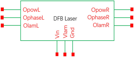
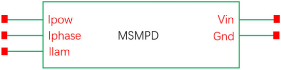
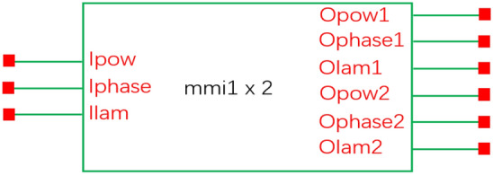
Our developed model library is implemented using Verilog-A and is compatible with SPICE simulations. Unlike earlier compact models that focus solely on optical power output, our model’s set of optical input and output ports includes three sub-portals expressing the power (W), phase ( ), and wavelength (m) of light, as depicted in Fig. 1. Building on this foundation, we have developed compact models for various lasers, photodetectors, modulators, other light sources, and passive components. Then we used the AetherPT optoelectronic simulation platform of Empyrean to build the schematic used to test the performance of the device, conducted a variety of simulations, and obtained several results. Additionally, we compared these outcomes with those documented in the literature and obtained via other software. This comparison confirmed that the fundamental attributes of each model in our library closely correspond to their real-world counterparts.
Fig. 1.

Schematic diagram of the optical ports of the device, with input ports on the left and output ports on the right.
Compact models of active devices
Lasers
Distribute feedback bragg laser
Our distribute feedback bragg (DFB) laser is based on the equivalent circuit model referenced in Ref7, which initiates with the traveling wave equations and subsequently derives the aforementioned equivalent circuit equations. In comparison to other laser models in the model library, this model accounts for the physical effects of grating coupling, end-plane reflections, and auger compounding of the DFB laser. Currently, the model does not include temperature and phase variations, both of which are slated for further investigation.
 |
1 |
 |
2 |
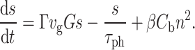
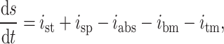
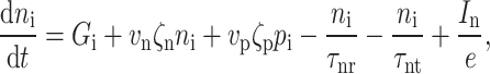
In the equation above, Eq. (1) represents the change in carrier (electron) concentration. Equation (2) details the change in photon concentration, which significantly influences the output optical power’s magnitude. In these equations, n is the excess carrier concentration in the active region,  is the current injected into the active region,
  is the volume of the active region,
  is the trap-assisted recombination lifetime,
  is the Auger recombination coefficient,
  is the radiative recombination coefficient, s is the photon density, G is the optical gain,
  is the optical confinement factor,
  is the spontaneous radiation coefficient,
  is the speed of light, and
  is the photon lifetime.The compact model of DFB laser is illustrated in Fig. 2.
Fig. 2.
Schematic diagram of a compact model of DFB laser.
The results used data from7 for the DFB laser are presented in Fig. 3, which illustrates the relationship between optical output and current for the DFB laser. The curve shows a linear increase with current above the threshold, reflecting the model’s exclusion of temperature effects on device performance. Figure 3b depicts the I-V relationship for the DFB laser, where the port voltage remains nearly constant above the threshold, indicating linear power increase. These results confirm that the model accurately represents the steady-state characteristics of the DFB laser, excluding temperature considerations. The frequency response of the DFB laser, shown in Fig. 3c, reveals a 3 dB bandwidth of approximately 3.21 GHz. We compared the optical output and frequency response with data from7, achieving favorable comparisons that underscore the model’s reliability. Figure 3d and e display the time-domain simulation results, with Fig. 3d focusing on the impulse response. The impulse response results indicate overshoot at both pulse edges. Figure 3e displays the eye diagram, indicating that overshoot is more pronounced near the threshold and significantly diminishes at higher currents. The MSE of the DC test is approximately  mW
mW , while the AC test is about 0.18 dB
 . These findings demonstrate that the laser model effectively simulates the steady-state and transient characteristics of DFB lasers and aligns well with documented frequency domain characteristics. In future work, we will integrate a temperature-dependent module to enhance the model’s fidelity to the actual device.
Fig. 3.

Schematic representation of the results for DFB laser. (a) and (b) shows DC test result and frequency response test result compare with7, (c) shows the variation of voltage with current at the input port, (d) shows impulse response test result and (e) shows eye diagram test result.
Vertical-cavity surface-emitting laser
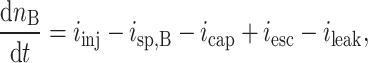
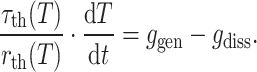
The vertical-cavity surface-emitting laser (VCSEL) in our model library utilizes the model referenced in Ref10, an equivalent circuit model specifically designed to simulate various physical effects such as spontaneous radiation and auger composite, along with the device’s temperature changes and their impacts on the power, wavelength, and other characteristics of the emitted light. Additionally, this model distinctively incorporates the resistance, inductance, and capacitance characteristics of the pads, wires, and non-illuminated areas, features absent from other models. The model also plans to investigate the effect of noise on device performance. It is constructed using the following equations:
 |
3 |
 |
4 |
 |
5 |
 |
6 |
In these equations, Eq. (3) denotes the change in carrier concentration in the SCH region, Eq. (4) represents the change in carrier concentration in the quantum well region, Eq. (5) signifies the change in photon concentration, and Eq. (6) expresses the change in temperature. In these equations,  represents the injected carrier concentration (related to the injection current),
  and
and  represent the spontaneous carrier recombination in the potential and quantum well regions,
  represents the trapping of carriers in the quantum well,
  represents the carriers escaping from the quantum well to the potential,
  represents the leakage in the SCH region,
  represents the excited carrier recombination,
  represents the luminescent part of the spontaneous emission,
  represents the absorption of free carriers,
  and
and  represent bottom and top losses.The compact model ofVCSEL is illustrated in Fig. 4.
Fig. 4.

Schematic diagram of a compact model of VCSEL.
Figure 5 presents the simulation results of the VCSEL derived from data in Ref10 and compares these with the reported findings. Figure 5a depicts the VCSEL’s optical output curve against current at various temperatures, demonstrating a linear relationship between optical power and current just above the threshold at low currents. Once the current surpasses the threshold, optical power growth slows and may even decrease due to thermal roll-back. Furthermore, higher room temperatures lower the thermal roll-back’s critical point. This occurs as higher temperatures shift the wavelength from the resonant wavelength, diminishing optical gain. Figure 5b illustrates the VCSEL’s I-V relationship, less influenced by temperature, where increasing current continuously boosts total power, converting substantial electrical energy into thermal energy, as depicted in Fig. 5c. Temperature fluctuations result in wavelength shifts, with Fig. 5d showing how wavelength changes with input current. The curve shape of wavelength changes with current mirrors that for temperature changes, suggesting a linear relationship with temperature, consistent with the model. Comparison results indicate minimal simulation errors for the I–V relationship, temperature, and wavelength at various temperatures. Optical power comparisons perform better at lower temperatures but show larger discrepancies at higher ones, suggesting significant scope for enhancing the model and its optical output parameters. These simulation results outline the threshold behavior, temperature effects, and thermal roll-back in optical output for the VCSEL, demonstrating the model’s reliability in steady-state simulations. Figure 5e and f display the time-domain simulation results. Figure 5e details the impulse response, while Fig. 5f examines the eye diagram, revealing initial and rising edge oscillations, as well as relaxation oscillations at each pulse’s falling edge in the laser model. The MSE of the DC tests at various temperatures ranges from approximately 0.003–0.06 mW , with corresponding voltage values ranging from 0.0007 to 0.0035 V
 , temperature values from
  to
to  , and wavelength values from 0.006 to 0.014 nm
 . These outcomes validate the model’s ability to accurately represent VCSEL characteristics in both steady-state and time-domain simulations, aligning well with real conditions.
Fig. 5.

Schematic representation of the results for VCSEL. (a) shows DC test result, (b) shows the variation of voltage with current at the input port, (c) shows temperature of VCSEL in response to current changes and (d) shows wavelength changes in response to current changes, in comparison with10 below. (e) Shows impulse response test result, and (f) shows PAM4 eye diagram test result.
Photodetectors
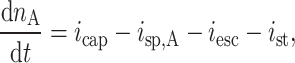
Much like lasers, our photodetector model is developed using an equivalent circuit model. The corresponding model’s equivalent circuit equations are derived by expressing the physical equations for the change in carrier concentration in circuit form.
PINAPD and PINPD
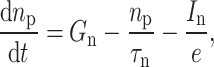
We utilized the equivalent circuit model referenced in Ref7 for the PIN avalanche photodiode (PINAPD). This model comprehensively models the generation, diffusion, drift, and compounding of carriers in each region of the detector; it also accounts for the impact ionization of carriers in the I-region, also known as the avalanche effect. For a PINPD without avalanche effects, setting the impact ionization rates ( and
and  ) to zero in these terms is sufficient. The physical equations used to construct the PINAPD are as follows:
 |
7 |
 |
8 |
 |
9 |
 |
10 |
In these equations, Eq. (7) describes the change in electron concentration in the P region, Eq. (8) details the change in hole concentration in the N region, and Eqs. (9) and (10) reflect changes in carrier concentration in the I region. Practically, only one of Eqs. (9) and (10) may be required for modeling.  (
( ) is the total number of excess holes (electrons) in N(P) region,
  (
( ) is the total number of excess electrons (holes) in I region,
  (
( ) is the lifetime of holes (electrons) in N(P) region,
  (
( ) is the recombination lifetime of electrons (holes) in I region,
  (
( ) is the drift time of electrons (holes) in I region,
  (
( ) is the rate of electron-hole pair production in N(P) region for incident light,
  is the rate of electron-hole pair production in I region for incident light,
  (
( ) is the minority carrier hole (electron) diffusion current in the N(P) region,
  (
( ) is the electron (hole) drift velocity in I region, and
  (
( ) is the collision ionization rate of the electron (hole) in I region. The compact model of PINAPD and PINPD are illustrated in Fig. 6.
Fig. 6.

Schematic diagram of a compact model of PINAPD and PINPD.
Using data from Ref7, we simulated the PINAPD, with results depicted in Fig. 7. Figure 7a illustrates the simulation results for the dark current, showing a minor initial dark current that escalates with bias voltage, particularly accelerating beyond 60 V. This surge in dark current is primarily attributed to leakage current. At approximately 80 V, as the bias increases further, an avalanche effect manifests. This avalanche effect arises from increased impact ionization rate due to the larger negative bias, generating significant avalanche current. The model’s accuracy is demonstrated by the minimal discrepancy between our results and those reported in7. Figure 7b presents the impulse response of the PINAPD, highlighting the model’s slow response to impulse signals and difficulty handling ultrafast signals. Figure 7c shows the eye diagram test results, indicating pronounced rising and falling edges of this detector’s signal, potentially causing loss of signal detail. These issues are likely due to slow carrier diffusion. These results verify that our detector model accurately simulates PINAPD’s physical effects, including the avalanche effect; however, its slow response to pulsed signals indicates the need for a more responsive model in future developments. The MSE of the DC test is approximately 1.98  .
.
Fig. 7.

Schematic representation of the results for PINAPD. (a) shows dark current test result in comparison with7, (b) shows impulse response test result, and (c) shows eye diagram test result.
MSMPD
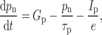
The metal-semiconductor-metal photodiode (MSMPD) possesses a simpler device structure, which consequently results in a simpler equation structure. The model accounts for carrier generation, drift, and compounding. The physical equations employed for this detector are as follows7:
 |
11 |
 |
12 |
Equation (11) describes changes in electron concentration, while Eq. (12) addresses changes in hole concentration. In these equations, n(p) is the total number of excess electrons (holes) in the absorption region,  (
( ) is the electron (hole) drift transition time,
  (
( ) is the electron (hole) recombination lifetime, and G is the number of photo-generated carriers produced per unit time in the absorption region, which is related to the input optical power.The compact model of MSMPD is illustrated in Fig. 8.
Fig. 8.
Schematic diagram of a compact model of MSMPD.
Data from7 were utilized for MSMPD simulation, with results depicted in Fig. 9. Figure 9a presents the photocurrent simulation. It illustrates that the current increases linearly with bias voltage at higher voltages. This linear increase is attributed to the MSMPD’s simple structure and lack of avalanche gain, resulting in a current primarily composed of photocurrent. Our results, compared with those in Ref7, align closely with expectations, thereby confirming the model’s reliability. Figure 9b depicts the impulse response, showing that the MSMPD responds more quickly to impulse signals than the PINAPD does. The optical signal drops immediately post-impulse, although signal waveform consistency is not assured. Figure 9c displays the eye diagram test results, indicating that this detector’s rising and falling edges are less pronounced than those of the PINAPD.The MSE of the DC test is approximately  . These findings demonstrate the model’s enhanced capability to simulate MSMPD properties.
Fig. 9.

Schematic representation of the results for MSMPD. (a) shows DC test result in comparison with7, (b) shows impulse response test result, and (c) shows PAM4 eye diagram test result.
Modulators
Our model library encompasses simple ideal modulators as well as complex modulators like the Mach–Zehnder modulator, electroabsorption modulator, ring resonator, and optical add-drop filter.
Ideal modulators
Our model library comprises ideal amplitude, phase, and frequency modulators. The equation for the ideal amplitude modulator is presented below:
 |
13 |
The equation for the ideal phase modulator is presented below:
 |
14 |
The equation for the ideal frequency modulator is presented below:
 |
15 |
In the above equations, d(t) is a function related to the input signal. These modulators are illustrated as shown in Fig. 10.
Fig. 10.

Schematic diagram of a compact model of ideal modulators, from left to right are amplitude, phase, and frequency modulators.
Multimode interference
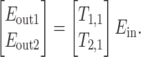
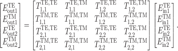
The multimode interference (MMI) is a crucial component used for beam combining, beam splitting, coupling, and building devices such as Mach–Zehnder modulators and ring resonators. We utilized the model referenced in Ref19, which advantageously captures the effects of each mode inside the MMI on the input optical signal at specific wavelengths and also describes the transmission losses within the MMI. For instance, modeling a 1  2 MMI is conducted as follows:
 |
16 |
The matrix in the middle of this equation represents the transmission matrix. As polarization is not considered, the inputs and outputs are only taken into account for one of the TE or TM modes, and the model neglects the coupling of the TE and TM modes. The form of the elements in the transmission matrix is as follows19:
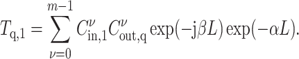 |
17 |
Where m is the total number of modes within the MMI device, q represents the number of the output port. The coupling coefficients  and
and  are derived through the integration over the input or output port and each internal mode. The propagation constant is denoted by
  , while
  represents the propagation loss. Lastly, L signifies the length of the MMI device. The model of the MMI is illustrated in Fig. 11.
Fig. 11.
Schematic diagram of a compact model of multimode interference.
We examined the variation in optical power with wavelength for a 1  2 MMI using data from Ref19, with results displayed in Fig. 12, which reveals that the optical output from a single port of the MMI increases with wavelength, peaks at approximately 1550 nm, and subsequently decreases. This pattern occurs because the wavelength influences the refractive index and propagation coefficient of each mode within the MMI. Additionally, wavelength shifts alter the number of modes in the MMI, causing the noticeable jump on the right side of Fig. 12. Furthermore, our results were compared with those in Ref19, yielding superior comparative outcomes. The MSE of the MMI is approximately
  . This demonstrates the model’s capability to accurately depict the physical properties of the MMI.
Fig. 12.

Schematic representation of the results for MMI in comparison with Ref19.
Mach–Zehnder modulator
We have constructed both an ideal Mach-Zehnder modulator and a variant of the Mach–Zehnder modulator wherein the refractive index changes with both wavelength and voltage signal. This advanced model, in contrast to those in other model libraries, enables the characterization of various operational states of the Mach–Zehnder modulator at different wavelengths, and simulates how variations in carrier concentration under stress influence the modulator’s performance. The behavior of an ideal Mach–Zehnder modulator is described by the following equations20:
 |
18 |
In the above equation, A is associated with attenuation,  and
and  are linked to the mixing difference between the two arms,
  and
and  affect the phase of the output, and these terms are connected to the voltage at the input port.
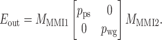
The Mach–Zehnder modulator, where the refractive index varies with both wavelength and voltage signal, referencing the modeling approach described in Ref19. This model comprises two multimode interference (MMI) devices and a voltage-controlled phase shifter, characterized by the following matrix calculation equation:
 |
19 |
Here,  and
and  represent the transmission matrices of the MMIs discussed in the preceding section,
  denotes the transmission coefficient of the phase shifter, and
  signifies the transmission coefficient of the waveguide in the opposing arm. The model of the aforementioned Mach–Zehnder modulator is illustrated in Fig. 13.
Fig. 13.

Schematic diagram of compact models of Mach–Zehnder modulator.
Using data from19, we simulated the Mach–Zehnder modulator. Figure 14a illustrates how the optical output of the Mach–Zehnder modulator varies with wavelength. The modulator model features two MMIs, a voltage-adjustable phase shifter in between, and a waveguide on the opposite arm. The MMIs modulate the optical output, peaking at 1550 nm. A discontinuity on the right side of the curve results from changes in the MMI’s mode count. Interference between the MMI-modulated light, the phase shifter, and the waveguide causes periodic changes in optical output, reflecting varying refractive indices at different wavelengths. Comparisons with simulation results from the software in Ref19 showed our results to be superior, affirming the model’s accuracy. Figure 14b presents the eye diagram test results, revealing a nonlinear response of optical output to negative bias due to nonlinear carrier concentration variations with bias. The MSE of the MMI is approximately  . These results confirm that the model effectively simulates the diverse characteristics of the Mach–Zehnder modulator.
Fig. 14.

(a) shows schematic representation of the results for Mach–Zehnder modulator in comparison with19 and (b) shows the PAM4 eye diagram for the Mach–Zehnder modulator in 1550 nm at voltages of 0V,  2 V,
2 V,  4 V, and
  6 V.
6 V.
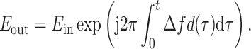
Electroabsorption modulator
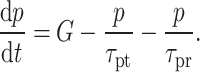
Our electroabsorption modulator is based on the model documented in Ref13. Unlike other models, it accounts for the changes in carrier concentration upon voltage application and more accurately depicts the alterations in output power and phase of the electroabsorption modulator. The behavioral equations of the electroabsorption modulator are as follows:
 |
20 |
 |
21 |
The above equations describe the power and phase variations of the electroabsorption modulator, with  and
and  being device-dependent functions. The model of the electroabsorption modulator is illustrated in Fig. 15.
Fig. 15.

Schematic diagram of a compact model of electroabsorption modulator.
Ring resonator and optical add-drop filter
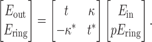
Most ring resonators in the model library consist merely of a coupler and phase shift and do not consider the impact of applied voltage. The ring resonators and optical add-drop filters in our model library consider the effects of wavelength and dispersion on device performance, along with the inherent losses of the ring. In a manner akin to the Mach–Zehnder modulator, we have constructed ring resonators where the refractive index changes with wavelength and voltage signals. The voltage-applied ring resonator facilitates calculating the carrier distribution and consequent changes in loss and refractive index, thereby affecting the device’s optical modulation. The basic ring resonator is constructed using a transmission matrix, which is employed as follows:
 |
22 |
As with MMI, the model’s inputs and outputs are designed to accommodate either the TE or TM modes exclusively, excluding coupled TE and TM modes. The form of the TE or TM mode propagation element in the transmission matrix is as follows21:
 |
23 |
In the above equation,  stands for TE mode or TM mode,
  is a coefficient related to the coupling of the straight waveguide and the ring,
  is a coefficient related to the propagation coefficient, attenuation, and phase shift of the ring, and
  is a coefficient related to the propagation coefficient and phase shift of the straight waveguide.
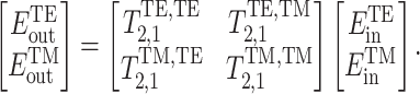
Similarly, the equation describing the optical add-drop filter can be derived from the transmission matrix:
 |
24 |
The structure of the terms in the transmission matrix resembles Eq. (23)21.
Additionally, we construct a model of a ring resonator, wherein the refractive index varies with both wavelength and voltage signal, based on the modeling methodology described in Ref19. This model consists of a coupler and a phase shifter, employed to simulate a ring resonator, with the matrix calculation as follows:
 |
25 |
where t denotes the transmission coefficient of the coupler,  represents the coupling coefficient, and p is associated with the modulation of light by the micro-ring. Various models of ring resonators are depicted as shown in the Fig. 16.
Fig. 16.

Schematic diagram of compact models of ring resonator and optical add-drop filter.
Data from22 were employed to simulate the variation in optical output with wavelength for the basic ring resonator and the optical add-drop filter. Figure 17a displays the basic ring resonator’s results, where the optical output shows periodic decay with wavelength due to the mutual coupling between the straight waveguide and the optical signal in the micro-ring. Figure 17b presents the optical add-drop filter’s results, illustrating that the port 2 output signal periodically peaks with wavelength, in contrast to the port 1 output, which shows periodic decay. This demonstrates successful signal coupling at the resonant wavelength into the alternate straight waveguide, enabling effective signal separation during multimode transmission. Additionally, we conducted identical simulations in VPI Photonics, and our model’s results closely align with the VPI Photonics’ findings. The MSE of the ring resonator is approximately  W
W , while the optical add-drop filter is about
  W
W and
and  W
W . These results affirm the accuracy of our model for the ring resonator with an optical add-drop filter.
Fig. 17.

(a) shows schematic representation of the results for ring resonator in comparison with22 and (b) shows schematic representation of the results for optical add-drop filter in comparison with22.
Additionally, we utilized data from the software described in Ref19 to simulate a ring resonator model featuring an externally adjustable bias voltage from our model library. Figure 18a illustrates the relationship between optical output and wavelength for this model under varying negative bias voltages. It shows not only the periodic decay of optical output with wavelength but also that the resonant wavelength and the decay wave’s valley expand as bias voltage increases, a result of the voltage-induced changes in the micro-ring’s refractive index. Our results were compared with the software simulations in Ref19, revealing good agreement across all bias voltages, thereby affirming our model’s reliability. Figure 18b presents the eye diagram test results, indicating that, like the Mach–Zehnder modulator, the ring resonator’s optical output reacts nonlinearly to negative bias, due to the bias’s nonlinear impact on carrier concentration. The MSE of the ring resonator at various voltages ranges from approximately 0.00027–0.0059 W . These results demonstrate that the model accurately simulates the ring resonator’s operating states under various bias voltages, aligning well with actual conditions.
Fig. 18.

(a) shows schematic representation of the results for ring resonator with multi voltage in comparison with19 and (b) shows PAM4 diagram of ring resonator in 1550 nm at voltages of 0 V,  2 V,
2 V,  4 V, and
  6 V.
6 V.
Passive components
Our model library includes compact models for passive components such as gain, phase shift, filter, jointer, splitter, coupler, etc., as well as simple waveguide models.
Gain, phase shift and filter
Gain, phase shift, and filter are relatively simple to implement. Gain devices mechanically scale the output power by adjusting the value of the gain coefficient. When the gain factor is less than one, it can be considered as analog optical attenuation. Phase shift devices change the phase of the output by varying the voltage input to the electrical port. Filters are devices that output only optical signals of a certain wavelength. These devices are modeled as shown in Fig. 19.
Fig. 19.

Schematic diagram of a compact model of gain, phase shift and filter.
Jointer and splitter
Jointers and splitters are utilized to combine multiple beams of light into a single beam or to split a beam into multiple beams. As an example of combining and splitting two beams of light, the jointer follows the equation:
 |
26 |
The splitter follows the equations:
 |
27 |
 |
28 |
The jointer and splitter for the two beams are modeled as illustrated in Fig. 20.
Fig. 20.

Schematic diagram of a compact model of jointer and splitter for the two beams.
Coupler
The coupler mixes the light input from both ports and outputs it. Our coupler utilizes the following matrix equation23:
 |
29 |
In the above equation, both p and c are adjustable parameters. The modeling based on this equation is illustrated in Fig. 21.
Fig. 21.
Schematic diagram of a compact model of coupler.
Waveguide
Our waveguide is modeled using the form of a transmission matrix, which currently supports only one mode of input and output, as polarization is not considered in the model library. The matrix equation used for this model is shown below:
 |
30 |
In the above equation, the matrix in the middle represents the transmission matrix. This matrix can be derived from the coupled equations24. The modeling based on this matrix equation is in Fig. 22.
Fig. 22.
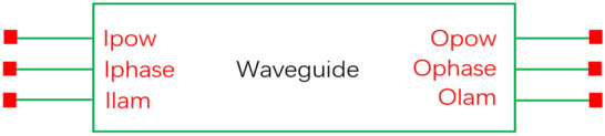
Schematic diagram of a compact model of waveguide.
Conclusion
We have developed an extensive compact model library that encompasses lasers, detectors, modulators, and various passive devices. The laser and detector models within this library are constructed using rate equations, while other models utilize transmission matrices or behavioral equations. Written in Verilog-A, the model library is compatible with SPICE simulation. We utilize Empyrean’s AetherPT platform along with diverse devices from our model library to construct simulation schematics, execute simulations, and compare outcomes with those documented in literature or from other software; these comparisons substantiate the accuracy and realism of our model library’s simulations. As we continue to expand the models within the library and enhance simulation accuracy, our future endeavors include incorporating optical polarization factors, noise, thermal effects, and other physical phenomena to align the simulation results more closely with reality. We anticipate the official release of the model library in mid-2024.
Acknowledgements
Zhigang Song discloses support for the research of this work from CAS Project for Young Scientists in Basic Research (YSBR-090), the National Key Research and Development Program of China (2021YFB2800304) and National Natural Science Foundation of China (62274190, 61934007).
Author contributions
G.C. developed this library, and was a major contributor in writing the manuscript. Z.S. proposed this idea and give funding support. X.Z. edited and refined the manuscript. All authors read and approved the final manuscript.
Data availability
Data sets generated during the current study are available from the corresponding author on reasonable request. The simulation parameters for the DFB laser, PINAPD, and MSMPD were obtained from 978-7-118-02330-2, the simulation parameters for the VCSEL were obtained from https://ieeexplore.ieee.org/document/9372754/, and the simulation parameters for the voltage-less ring resonator and the optical add-drop filter were obtained from https://ieeexplore.ieee.org/document/10431798/, and the simulation parameters for the voltage-added ring resonator, MMI, and Mach–Zehnder modulator were obtained from https://ieeexplore.ieee.org/document/8675505/.
Declarations
Competing interests
The authors declare no competing interests.
Footnotes
Publisher’s note
Springer Nature remains neutral with regard to jurisdictional claims in published maps and institutional affiliations.
Contributor Information
Zhigang Song, Email: songzhigang@semi.ac.cn.
Xinhe Zheng, Email: xinhezheng@ustb.edu.cn.
References
- 1.Bogaerts, W. & Chrostowski, L. Silicon photonics circuit design: Methods, tools and challenges. Laser Photon. Rev.12, 1700237. 10.1002/lpor.201700237 (2018). [Google Scholar]
- 2.Shawon, M. J. & Saxena, V. Rapid simulation of photonic integrated circuits using Verilog-A compact models. IEEE Trans. Circuits Syst. I Regular Papers67, 3331–3341. 10.1109/TCSI.2020.2983303 (2020). [Google Scholar]
- 3.Ren, F. et al. Compact modeling and photoelectric co-simulation of hybrid BICMOS-photonic segmented-electrode MZM transmitter. In 2020 IEEE 5th International Conference on Integrated Circuits and Microsystems (ICICM), 101–104, 10.1109/ICICM50929.2020.9292264 (IEEE, Nanjing, China, 2020).
- 4.Pelloux-Prayer, J. & Moradi, F. Compact model of all-optical-switching magnetic elements. IEEE Trans. Electron Devices67, 2960–2965. 10.1109/TED.2020.2991330 (2020). [Google Scholar]
- 5.Tucker, R. S. Circuit model of double-heterojunction laser below threshold. IEE Proc. I Solid State Electron Devices128, 101. 10.1049/ip-i-1.1981.0029 (1981). [Google Scholar]
- 6.Gao, Jianjun. High Speed Optoelectronic Device Modeling and Integrated Circuit Design (Higher Education Press, Beijing, 2009). [Google Scholar]
- 7.Chen, Weiyou. Optoelectronic Devices Circuit Model and The Circuit-level Simulation of OEIC (National Defense Industry Press, Arlington, 2001). [Google Scholar]
- 8.Nie, B. et al. Circuit model for the effect of nonradiative recombination in a high-speed distributed-feedback laser. Curr. Opt. Photon.4, 434–440. 10.3807/COPP.2020.4.5.434 (2020). [Google Scholar]
- 9.Kim, Byoung-Sung., Chung, Youngchul & Lee, Jae-Seung. An efficient split-step time-domain dynamic modeling of DFB/DBR laser diodes. IEEE J. Quantum Electron.36, 787–794. 10.1109/3.848349 (2000). [Google Scholar]
- 10.Grabowski, A., Gustavsson, J., He, Z. S. & Larsson, A. Large-signal equivalent circuit for datacom VCSELs. J. Lightwave Technol.39, 3225–3236. 10.1109/JLT.2021.3064465 (2021). [Google Scholar]
- 11.Mukherjee, C. et al. SPICE modeling in Verilog-A for photo-response in UTC-photodiodes targeting beyond-5G circuit design. IEEE Trans. Comput. Aided Des. Integr. Circuits Syst.42, 3045–3052. 10.1109/TCAD.2023.3236277 (2023). [Google Scholar]
- 12.Dalla Mora, A., Tosi, A., Tisa, S. & Zappa, F. Single-photon avalanche diode model for circuit simulations. IEEE Photon. Technol. Lett.19, 1922–1924. 10.1109/LPT.2007.908768 (2007). [Google Scholar]
- 13.Cheng, N. & Cartledge, J. Measurement-based model for MQW electroabsorption modulators. J. Lightwave Technol.23, 4265–4269. 10.1109/JLT.2005.858217 (2005). [Google Scholar]
- 14.Lewen, R., Irmscher, S., Westergren, U., Thylen, L. & Eriksson, U. Segmented transmission-line electroabsorption modulators. J. Lightwave Technol.22, 172–179. 10.1109/JLT.2003.822829 (2004). [Google Scholar]
- 15.Wang, B. et al. A compact verilog-a model of silicon carrier-injection ring modulators for optical interconnect transceiver circuit design. J. Lightwave Technol.34, 2996–3005. 10.1109/JLT.2015.2505239 (2016). [Google Scholar]
- 16.Wu, R. et al. Compact models for carrier-injection silicon microring modulators. Opt. Express23, 15545. 10.1364/OE.23.015545 (2015). [DOI] [PubMed] [Google Scholar]
- 17.Kocabas, S., Veronis, G., Miller, D. & Fan, S. Transmission line and equivalent circuit models for plasmonic waveguide components. IEEE J. Sel. Top. Quantum Electron.14, 1462–1472. 10.1109/JSTQE.2008.924431 (2008). [Google Scholar]
- 18.James, A. et al. Process Variation-Aware Compact Model of Strip Waveguides for Photonic Circuit Simulation. Journal of Lightwave Technology 1–14, 10.1109/JLT.2023.3238847 (2023). ArXiv:2301.01689
- 19.Chen, X. et al. Modeling and analysis of optical modulators based on free-carrier plasma dispersion effect. IEEE Trans. Comput. Aided Des. Integr. Circuits Syst.39, 977–990. 10.1109/TCAD.2019.2907907 (2020). [Google Scholar]
- 20.Chuang, S. L. Physics of Photonic Devices. Wiley Series in Pure and Applied Optics 2nd edn. (Wiley, Hoboken, 2009). [Google Scholar]
- 21.Yariv, A. Universal relations for coupling of optical power between microresonators and dielectric waveguides. Electron. Lett.36, 321. 10.1049/el:20000340 (2000). [Google Scholar]
- 22.Ming, D. et al. EPHIC models: General spice photonic models for closed-loop electronic-photonic co-simulation. IEEE Trans. Circuits Syst. I Regular Papers[SPACE]10.1109/TCSI.2024.3353459 (2024). [Google Scholar]
- 23.Keiser, G. Optical Fiber Communications Vol. 4 (McGraw-Hill, New York, 2011). [Google Scholar]
- 24.Huang, W.-P. Coupled-mode theory for optical waveguides: An overview. J. Opt. Soc. America A11, 963. 10.1364/JOSAA.11.000963 (1994). [Google Scholar]
Associated Data
This section collects any data citations, data availability statements, or supplementary materials included in this article.
Data Availability Statement
Data sets generated during the current study are available from the corresponding author on reasonable request. The simulation parameters for the DFB laser, PINAPD, and MSMPD were obtained from 978-7-118-02330-2, the simulation parameters for the VCSEL were obtained from https://ieeexplore.ieee.org/document/9372754/, and the simulation parameters for the voltage-less ring resonator and the optical add-drop filter were obtained from https://ieeexplore.ieee.org/document/10431798/, and the simulation parameters for the voltage-added ring resonator, MMI, and Mach–Zehnder modulator were obtained from https://ieeexplore.ieee.org/document/8675505/.