Abstract
We report free-standing atomic crystals that are strictly 2D and can be viewed as individual atomic planes pulled out of bulk crystals or as unrolled single-wall nanotubes. By using micromechanical cleavage, we have prepared and studied a variety of 2D crystals including single layers of boron nitride, graphite, several dichalcogenides, and complex oxides. These atomically thin sheets (essentially gigantic 2D molecules unprotected from the immediate environment) are stable under ambient conditions, exhibit high crystal quality, and are continuous on a macroscopic scale.
Keywords: graphene, layered material
Dimensionality is one of the most defining material parameters; the same chemical compound can exhibit dramatically different properties depending on whether it is arranged in a 0D, 1D, 2D, or 3D crystal structure. Although quasi-0D [e.g., cage molecules (1)], quasi-1D [e.g., nanotubes (2-4)], and, of course, 3D crystalline objects are well documented, dimensionality two is conspicuously absent among experimentally known crystals. On the other hand, there are many layered materials with strong in-plane bonds and weak, van der Waals-like coupling between layers. Because of this layered structure, it has long been tempting to try splitting such materials into individual atomic layers, although it remained unclear whether free-standing atomic layers could exist in principle [thin films become thermodynamically unstable (decompose or segregate) below a certain thickness, typically, of many dozens layers]. Thus far, most efforts have focused on chemical exfoliation of strongly layered materials and, in particular, of stage I intercalated graphite (5). During exfoliation, monolayers at some moment must separate from each other. However, no 2D crystals have ever been isolated from the resulting slurries, possibly because single layers appear only as a transient state and involve detachments over microscopic regions. Indeed, the latest studies of chemically exfoliated graphite have shown that its sediments consist of restacked and scrolled multilayer sheets rather than individual monolayers (6-8). An alternative approach has been the use of mechanical cleavage (9-14). The earlier reports described mechanically cleaved flakes consisting of tens and hundreds of layers, but the recently renewed interest in thin graphitic films led to flaky materials with a thickness of just a few graphene layers (12-15). Now we have extended the approach to its ultimate limit: We have isolated individual crystal planes from a large variety of strongly layered materials and shown that the resulting 2D crystals exhibit high crystal quality and macroscopic continuity.
Materials and Methods
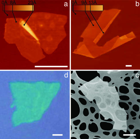
Fig. 1 shows several examples of cleaved samples and illustrates that they are only one atomic layer thick but nearly macroscopic laterally. To extract such 2D crystallites, we used a simple but effective procedure. A fresh surface of a layered crystal was rubbed against another surface (virtually any solid surface is suitable), which left a variety of flakes attached to it (the rubbing process can be described as similar to “drawing by chalk on a blackboard”). Unexpectedly, among the resulting flakes we always found single layers. Their preliminary identification amid thicker flakes and other residue was done in an optical microscope. 2D crystallites become visible on top of an oxidized Si wafer (Fig. 1d), because even a monolayer adds up sufficiently to the optical path of reflected light so that the interference color changes with respect to the one of an empty substrate (phase contrast). The whole procedure takes literally half an hour to implement and identify probable 2D crystallites. Their further analysis was done by atomic force microscopy (AFM), for which single-layer crystals were selected as those exhibiting an apparent (12) thickness of approximately the interlayer distance in the corresponding 3D crystals.
Fig. 1.
2D crystal matter. Single-layer crystallites of NbSe2 (a), graphite (b), Bi2Sr2CaCu2Ox (c), and MoS2 (d) visualized by AFM (a and b), by scanning electron microscopy (c), and in an optical microscope (d). (All scale bars: 1 μm.) The 2D crystallites are on top of an oxidized Si wafer (300 nm of thermal SiO2) (a, b, and d) and on top of a holey carbon film (c). Note that 2D crystallites were often raised by an extra few angstroms above the supporting surface, probably because of a layer of absorbed water. In such cases, the pleated and folded regions seen on many AFM images and having the differential height matching the interlayer distance in the corresponding 3D crystals help to distinguish between double-layer crystals and true single sheets such as those shown here.
Despite its simplicity, the described cleavage technique has several nonobvious features that are instructive to analyze, because it also allows one to understand why 2D crystals were not discovered earlier (e.g., see refs 9-11, 13, and 14, in which mechanically cleaved graphitic flakes 10-100 layers thick were reported). First, monolayers are in a great minority among accompanying thicker flakes. Second, unlike nanotubes, 2D crystals have no clear signatures in transmission electron microscopy (6-8). Third, monolayers are completely transparent to visible light and cannot be seen in an optical microscope on most substrates (e.g., on glass or metals). Fourth, AFM is currently the only method that allows definitive identification of single-layer crystals, but it has a very low throughput (especially for the case of the high-resolution imaging required), and in practice it would be impossible to find cleaved 2D crystallites by scanning surfaces at random. Finally, as mentioned earlier, it was not obvious that isolated atomic planes could survive without their parent crystals [for example, mechanically cleaved quasi-1D NbSe3 crystallites ≈100 nm in diameter were found to deteriorate rapidly (16)]. With the benefit of hindsight, the critical step that allowed us to find 2D crystallites is the discovered possibility of their tentative identification in an optical microscope when they are placed on top of an oxidized Si wafer.
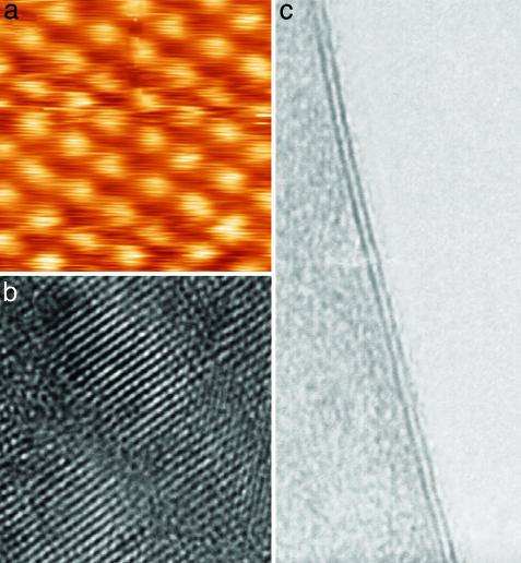
Representative samples of several 2D materials (namely, of BN, MoS2, NbSe2, Bi2Sr2CaCu2Ox, and graphite) obtained and identified by the procedures described above were investigated further by scanning tunneling, scanning electron, and high-resolution transmission electron microscopy (HRTEM). Fig. 2 shows examples of the obtained atomic-resolution images. These studies§ confirmed that the prepared 2D crystallites remained monocrystalline under ambient conditions and no degradation was noticed over periods of many weeks. Within experimental resolution, the crystal structure of isolated layers remained the same as for stacked layers within 3D crystals. Note that 2D Bi2Sr2CaCu2Ox showed a superstructure with a unidirectional modulation period of ≈28 Å, which is similar to the superstructure observed in thinned samples of bulk Bi2Sr2CaCu2Ox prepared for HRTEM (17).
Fig. 2.
Atomic-resolution images of 2D materials. (a) Unfiltered scanning tunneling microscopy image of the crystal lattice in the NbSe2 monolayer on top of an oxidized Si wafer. Note that for the scanning tunneling microscopy measurements, an Au film was deposited around 2D crystallites to provide an electrical contact. (b) HRTEM images of the 2D Bi2Sr2CaCu2Ox crystal shown in Fig. 1c. (c) HRTEM image of a double-layer MoS2. This image is shown to make a connection between our approach based on AFM identification of 2D crystals and the traditional HRTEM approach used for quasi-1D crystals (all nanotubes were first found by using HRTEM, where dark lines indicating the nanotube's walls parallel to the electron beam are easily visible). No similar signature exists for 2D crystals (see refs. 6-8), and we also found it difficult to align 2D samples exactly parallel to the electron beam. However, for two-layer crystals, their thickness is easily identifiable not only in AFM but also in HRTEM because of folded regions seen as two dark lines (in the case of c, the separation is ≈6.5 Å, in agreement with the interlayer distance in bulk MoS2). We occasionally observed short dark lines (compare with ref. 8) that might be folded monolayers, but no independent proof for this (e.g., by simultaneous AFM studies) has been obtained yet.
Results and Discussion
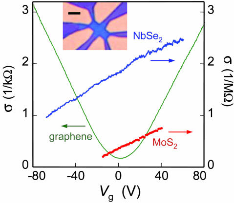
We also investigated electrical conductivity of the selected five 2D materials to assess their microscopic quality and macroscopic continuity. This was done by using field-effect-transistor-like devices such as the one shown in Fig. 3 Inset (devices were prepared by electron-beam lithography). 2D Bi2Sr2CaCu2Ox and BN were found to be highly insulating, and no induced conductivity was detected even at gate electric fields as high as 0.3 V/nm (i.e., close to the electrical breakdown of SiO2), which probably indicates that band gaps in these 2D materials are larger than in SiO2. We also tried annealing single-layer Bi2Sr2CaCu2Ox in oxygen, but the crystals always remained insulating.
Fig. 3.
Electric field effect in single-atomic-sheet crystals. Changes in electrical conductivity σ of 2D NbSe2, 2D MoS2, and graphene as a function of gate voltage are shown (300 K). (Inset) Our typical devices used for such measurements: It is an optical image (in white light) of 2D NbSe2 on top of an oxidized Si wafer (used as a gate electrode) with a set of Au contacts. The crystal is seen as a bluer region in the center. (Scale bar: 5 μm.)
On the contrary, 2D graphite (graphene) and both 2D dichalcogenides were found to be metallic and exhibited a pronounced electric field effect (Fig. 3). Their carrier mobilities were determined as μ = σ(Vg)/en(Vg), where e is the electron charge and n ∝ Vg is the carrier concentration induced by gate voltage Vg (n ≈ 7.2 × 1010 cm-2/V for 300-nm SiO2). As seen in Fig. 3, σ was proportional to Vg over large intervals of n, showing that μ is independent of carrier concentration. Furthermore, by extrapolating the experimental dependences σ(Vg) to zero σ, we could determine initial (Vg = 0) concentrations of charge carriers and their type. Graphene behaved rather similarly to few-layer graphitic samples reported in ref. 12 and is either a shallow-gap semiconductor or a small-overlap semimetal, in which positive and negative gate voltages induce 2D electrons and holes, respectively, in concentrations up to ≈1013 cm-2. Graphene exhibited typical values of μ between 2,000 and 5,000 cm2/Vs. For 2D NbSe2 and MoS2, we measured mobilities between 0.5 and 3 cm2/Vs for different samples, in agreement with mobilities for the corresponding 3D crystals at room temperature. Both 2D dichalcogenides were found to be electron conductors with n ≈ 1012 to 1013 cm-2. Detailed studies of their conductivities as a function of temperature and Vg revealed that 2D MoS2 was a heavily doped semiconductor with an activation gap of ≥0.6 eV, whereas NbSe2 was a semimetal. The found electron concentration in 2D NbSe2 is two orders of magnitude smaller than carrier concentrations per monolayer in 3D NbSe2, which indicates significant changes in the energy spectrum of NbSe2 from a normal metal in 3D to a semimetal in 2D.
In conclusion, we have demonstrated the existence of 2D atomic crystals that can be prepared by cleavage from most strongly layered materials. It is most unexpected, if not counterintuitive, that isolated 2D crystals can be stable at room temperature and in air, leaving aside the fact that they maintain macroscopic continuity and such high quality that their carrier mobilities remain almost unaffected. The found class of 2D crystals offers a wide choice of new materials parameters for possible applications and promises a wealth of new phenomena usually abundant in 2D systems. We believe that, once investigated and understood, 2D crystals can also be grown in large sizes required for industrial applications, matching the progress achieved recently for the case of single-wall nanotubes (18).
Acknowledgments
We thank P. B. Kenway for help with transmission electron microscope studies. This work was supported by the Engineering and Physical Sciences Research Council (United Kingdom). K.S.N. acknowledges The Leverhulme Trust for financial support.
This paper was submitted directly (Track II) to the PNAS office.
Abbreviations: AFM, atomic force microscopy; HRTEM, high-resolution transmission electron microscopy.
Footnotes
In the case of HRTEM studies [we used an FEI (Eindhoven, The Netherlands) Tecnai F30], the cleaved material was deposited directly on holey carbon films, which made the described route of preliminary identification of 2D crystallites in an optical microscope impossible. To find them on top of holey carbon among thicker flakes, a different procedure was developed. First, we used scanning electron microscopy imaging at low acceleration voltages (FEI Sirion at 500 V). Then, the flakes that were found most transparent in scanning electron microscopy were studied by AFM (i.e., directly on top of holey carbon) to define their thickness and select single-layer crystals.
References
- 1.Kroto, H. W., Fischer, J. E. & Cox, D. E., eds. (1993) The Fullerenes (Pergamon, Oxford).
- 2.Iijima, S. (1991) Nature 354, 56-58. [Google Scholar]
- 3.Chopra, N. G., Luyken, R. J., Cherrey, K., Crespi, V. H., Cohen, M. L., Louie, S. G. & Zettl, A. (1995) Science 269, 966-967. [DOI] [PubMed] [Google Scholar]
- 4.Tenne, R., Margulis, L., Genut, M. & Hodes, G. (1992) Nature 360, 444-446. [Google Scholar]
- 5.Dresselhaus, M. S. & Dresselhaus, G. (2002) Adv. Phys. 51, 1-186. [Google Scholar]
- 6.Shioyama, H. (2001) J. Mater. Sci. Lett. 20, 499-500. [Google Scholar]
- 7.Viculis, L. M., Mack, J. J. & Kaner, R. B. (2003) Science 299, 1361. [DOI] [PubMed] [Google Scholar]
- 8.Horiuchi, S., Gotou, T., Fujiwara, M., Asaka, T., Yokosawa, T. & Matsui, Y. (2004) Appl. Phys. Lett. 84, 2403-2405. [Google Scholar]
- 9.Ebbesen, T. W. & Hiura, H. (1995) Adv. Mater. 7, 582-586. [Google Scholar]
- 10.Ohashi, Y., Hironaka, T., Kubo, T. & Shiiki, K. (1997) Tanso 180, 235-238. [Google Scholar]
- 11.Lu, X., Huang, H., Nemchuk, N. & Ruoff, R. S. (1999) Appl. Phys. Lett. 75, 193-195. [Google Scholar]
- 12.Novoselov, K. S., Geim, A. K., Morozov, S. V., Jiang, D., Zhang, Y., Dubonos, S. V., Grigorieva, I. V. & Firsov, A. A. (2004) Science 306, 666-669. [DOI] [PubMed] [Google Scholar]
- 13.Zhang, Y., Small, J. P., Amori, M. E. S. & Kim, P. (2005) Appl. Phys. Lett. 86, 073104. [Google Scholar]
- 14.Bunch, J. S., Yaish, Y., Brink, M., Bolotin, K. & McEuen, P. L. (2005) Nano Lett. 5, 287-290. [DOI] [PubMed] [Google Scholar]
- 15.Berger, C., Song, Z., Li, T., Li, X., Ogbazghi, A. Y., Feng, R., Dai, Z., Marchenkov, A. N., Conrad, E. H., First P. N. & de Meer, W. A. (2004) J. Phys. Chem. B 108, 19912-19916. [Google Scholar]
- 16.Slot, E., Holst, M. A., van der Zant, H. S. J. & Zaitzev-Zotov, S. V. (2004) Phys. Rev. Lett. 93, 176602. [DOI] [PubMed] [Google Scholar]
- 17.Shaw, T. M., Shivashankar, S. A., La Placa, S. J., Cuomo, J. J., McGuire, T. R., Roy, R. A., Kelleher, K. H. & Yee, D. S. (1988) Phys. Rev. B Condens. Matter. 37, 9856-9859. [DOI] [PubMed] [Google Scholar]
- 18.Zheng, L. X., O'Connell, M. J., Doorn, S. K., Liao, X. Z., Zhao, Y. H., Akhadov, E. A., Hoffbauer, M. A., Roop, B. J., Jia, Q. X., Dye, R. C., et al. (2004) Nat. Mater. 3, 673-676. [DOI] [PubMed] [Google Scholar]


