

Abstract
This paper proposes a non-isolated high step-up switched-capacitor dual-switch DC-DC converter for low-power applications. The proposed converter benefits from high voltage gain, low voltage stress on the devices, continuous input current, availability of common-ground point, and simple structure. The proposed converter provides the voltage gain of 10 at mild duty cycle of 50%, where the per-unit voltage stress of S1 and S2 switches are 20 and 40%, respectively. In such condition, the highest voltage stress on the diodes will be limited to 67%. The synchronous operation of the switches in proposed converter leads to only 2 operational modes in continuous conduction mode (CCM), which makes the control of the converter very straightforward. The interleaved structure divides the input current between the inductors, which accordingly reduces the losses on the input devices. This study contains detailed steady-state analysis of proposed converter in CCM and DCM operations. It also provides the loss (and efficiency) analysis as well as the design procedure of the devices. The comparison section evaluates the competitiveness of the proposed converter compared to other existing similar counterparts. The average state-space method and small signal analysis have been used to model the proposed topology. The appropriate dynamic operation of proposed converter has been verified by simulation analysis. The experimental results confirm the correct performance of the proposed converter.
Keywords: Common-grounded, Continuous input-current, High gain, Non-isolated DC-DC converter, Voltage stress
Subject terms: Electrical and electronic engineering, Renewable energy
Introduction
In recent years, the increase in demand for energy supply has led to an excessive increase in the consumption of fossil fuels, which has caused serious problems such as global warming, environmental pollution, and the reduction of reserves of this type of energy resources. Therefore, energy transition from fossil fuel sources to renewable sources is essential. Solar and wind energies are clean, renewable, vast and free. These features have made them very popular among renewable energy sources1,2.
Generally, due to the production of low DC output voltage by PV panels, it is necessary to use DC-DC converters to increase the voltage. The maximum power point tracking of the PV panel is also realized by the DC-DC converter. For this purpose, the DC-DC converter must have continuous input current3,4. In addition, to eliminate the leakage current of the PV panel, the DC-DC converter should possess common ground point5. The DC-DC converters are divided into isolated and non-isolated categories6,7. Isolated converters have a transformer, which increases safety, but leads to increased volume, weight, and cost, and reduced overall efficiency6,7. On the other hand, non-isolated converters have advantages such as simple, compact, and cheap structure, with higher efficiency, while their safety is lower than isolated converters due to the lack of isolation between input and output8. In this study, only non-isolated DC-DC converters are investigated. In recent decades, extensive research has been carried out in the field of providing new configurations for DC-DC converters with the aim of improving the voltage gain7–9. Besides the high voltage gain, there are other important features that should be considered, such as: low voltage stress on switching devices, ripple-free or low-ripple continuous input current, low current stress of semiconductors, reduced number of devices, simplicity and reliability of the structure, existence of the common ground point, and the low number of working modes that leads to the simplicity of the converter control10,11.
A widely used method to increase voltage gain in DC-DC converters is to use switched-capacitor network(s)12–23. The topology presented in12 is a dual-switch active-switched-inductor-network based converter that provides relatively high voltage gain, but lacks common ground point and suffers from high current stress of its switching elements. In13, the switched-capacitor network is used in a way that stores the energy of the active switched-inductor (A-SL) network and transfers it to the load. There is no common ground point in this structure. The voltage gain is also controlled by two duty cycles, which increases the number of operational modes and complexity of the control strategy. The structure presented in14 is combination of capacitor-diode network(s) with active switched-inductor based converter, which lacks common ground point. This structure, not only improves the voltage gain, but also tackles the capacitors’ impulsive charging/discharging currents issue. Other similar structures are presented in15, which are the extended version of14. In these structures, multiple capacitor-diode cells are utilized, which improves the boosting ability of the converter, but leads to increased number of required elements, too. The common-ground point is also missed in15. A common-grounded two-switch step-up topology is presented in16, whose duty cycle range is limited to 0.5. Another two-switch common-grounded quasi-Z-source converter is presented in17, where the duty cycle range is narrow (less than 0.25) and three semiconductors have to tolerate a voltage stress equal to output voltage. Also, switch S2 suffers from large current stress. Several high gain converters are presented in18 that utilize voltage pumping cells. Some of these converters suffer from pulsating source current or missed common-ground point. In19, a switched-capacitor network based multiphase step-up converter is presented, which takes advantage of high voltage gain, low voltage stress on the devices and low input current ripple. On the other hand, the large number of used elements leads to increased weight, volume and cost of converter. This structure also lacks the common-ground point. The topology presented in20 combines active-switched-inductor-network with switched-capacitor cells to provide high boosting factor, which still benefits from common-ground point. In21, a single-switch switched-capacitor based structure is presented that profits from low voltage stress on the switch, but lacks high step-up capability and common ground point. A generalized multi-stage single-switch switched-capacitor-inductor-network based converter is presented in22, whose switch suffers from large current stress. Moreover, as the number of networks increases, the voltage-drop on devices as well as the losses increase, too. Another generalized interleaved (multi-phase) common-grounded topology is presented in23 that provides high step-up capability, but suffers from high voltage stress on its output diode. Other similar topologies presented in24–30 will be fully investigated in comparison section (Section V).
This paper proposes a non-isolated dual-switch topology that profits from large step-up capability, continuous source current, low voltage stress on devices and common-ground point. Moreover, its interleaved nature leads to reduced losses and improved efficiency. The synchronous operation of switches results in minimum (two) operational modes, which eases the control of converter. The proposed topology is not a ripple-free converter. Due to the synchronous (simultaneous) charge/discharge of inductors, the input source current contains some ripple, which can be restricted by proper design of inductors.
The proposed converter, its operational principles as well as steady-state analysis are presented elaborated in the following section. The elements’ design procedure is provided in section III. Section IV yields the loss and efficiency analysis. In section V, the proposed converter is compared with similar existed counterparts. The outcomes of experimental analysis are presented in section VI. The average state-space model of proposed converter is presented in Section VII. Section VIII concludes the paper.
Proposed converter and its operation
Proposed configuration
Figure 1 shows the circuit configuration of proposed switched-capacitor based DC-DC converter that is constituted of 2 switches (S1-S2), 4 diodes (D1-D4), 2 inductors (L1-L2), and 4 capacitors (C1-C4). Owing to the interleaved feature, the source current is divided between the inductors, which may lead to reduced voltage drop and loss on the input-side devices.
Fig. 1.

Circuit configuration of proposed DC-DC converter.
Operational modes during CCM
The synchronous operation of switches in proposed converter leads to dual operational modes in continuous conduction mode (CCM), which are explained in the following.
Mode 1 [0-DT]
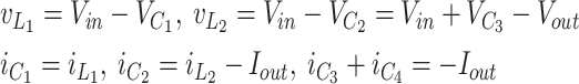
According to Fig. 2a, during first mode, both the switches and D3 conduct, while the other diodes are reverse-biased and off. In this mode, L1 is charged by Vin, where L2 is charged by the source and C1. Capacitor C3 is also charged by C1 and C2 through S1, S2 and D3. Capacitors C2 and C4 feed the load. The valid equations of 1st mode are as (1).
 |
1 |
Fig. 2.

Equivalent circuit of proposed converter during (a) mode 1 (CCM & DCM), (b) mode 2 (CCM & DCM).
Mode 2 [DT-T]
As seen from Fig. 2b, both the switches are turned off in second mode. Diode D3 is reverse-biased (off), while the other diodes are in the forward-biased (conducting) mode. Capacitor C1 is charged by the source and L1. Also, C2 is charged by the source and L2. Furthermore, C4 is charged by C3. The equations of this mode are shown in (2).
 |
2 |
Figure 3 shows the key waveforms of the proposed converter during CCM, where T: switching period, D: duty cycle, f(= 1/T): switching frequency.
Fig. 3.

Key waveforms during CCM, and DCM operations.
Steady-state analysis during CCM operation
Ideal voltage gain (MIdeal, CCM)
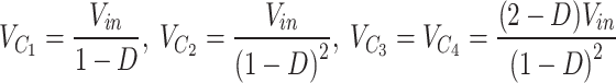
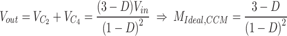
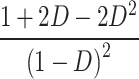
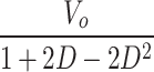
The voltage across the capacitors can be achieved by applying volt-second principle on the inductors, as (3)31. The relationship between the input and output voltages, as well as the ideal voltage gain (MIdeal, CCM) of proposed converter are as (4).
 |
3 |
 |
4 |
Voltage stress across the semiconductors
The voltage stress across the switching devices is shown in (5). For a clearer understanding, Fig. 4 shows the per unit voltage stress on the semiconductors, too. As seen, across practical range of duty cycle (around [0.2–0.8]), the per-unit of voltage stress on the switching devices is always much less than the unity.
Fig. 4.

Semiconductors’ voltage stress (in P.U.) vs. duty cycle.
 |
5 |
Inductors’ average current
The inductors’ average current can be obtained through employment of ampere-second balance principle on capacitors, which states that the average current of capacitor during a switching cycle is zero31. Accordingly, inductors’ average currents are achieved as (6).
 |
6 |
Inductors’ current ripple
The inductors’ current ripple can be calculated through (7).
 |
7 |
Inductors’ maximum/minimum currents
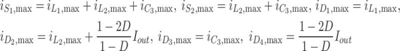
The inductors’ maximum/minimum current values are obtained through (8).
 |
8 |
Current stress of semiconductors
The current stress of semiconductors is shown in (9).
 |
9 |
Operational modes and steady-state analysis in DCM
The proposed topology is capable of operating in either of Continuous Conduction Mode (CCM), Boundary Conduction Mode (BCM) or Discontinuous Conduction Mode (DCM), based on the user’s preference. To keep the comprehensiveness of the paper, the DCM analysis are also presented. The proposed converter has four operational modes in DCM, as shown in (Fig. 3b). The initial two modes (Mode 1 [0-DT], Mode 2 [DT –d1T]) are exactly the same as the CCM operation. The remaining modes are elaborated in the following (shown in Fig. 5).
Fig. 5.

Equivalent circuit of proposed converter during (a) mode 3 (DCM), (b) mode 4 (DCM).
Mode 3 [d1T-d2T] (Fig. 5a)
The inductor L2 becomes completely discharged (iL2=0) at t = d1T. During this mode, the capacitor C1 continues to be charged by the input source and L1 (as (10)). The load is also supplied by C2 and C4 capacitors.
 |
10 |
Mode 4 [d2T-T] (Fig. 5b)
The inductor L1 is completely depleted (iL1=0) at t = d2T, as (11). The capacitors C2 and C4 keep on feeding the load.
 |
11 |
By applying volt-second principle on inductors, capacitors’ voltage during DCM operation are obtained as (12)31.
 |
12 |
The voltage gain (M) during DCM is calculated from (13).
 |
13 |
The inductors’ average current during DCM operation can be computed from (14).
 |
14 |
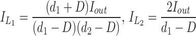
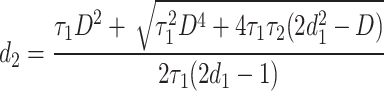
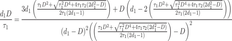
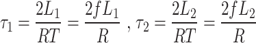
The relationships between duty cycle (D), d1 and d2 are presented in (15)-(16), where τ1 and τ2 are computed from (17).
 |
15 |
 |
16 |
 |
17 |
Where, T: switching period, and f: switching frequency. Having the duty cycle (D), the d1 and d2 can be computed by solving the (15), (16).
Real gain during CCM
The real gain of proposed converter during CCM operation and in presence of parasitic elements including on-state resistance of switches (rS), on-state resistance and forward voltage drop of diodes (rD, Vfd), and Equivalent Series Resistance (ESR) of capacitors and inductors (rC, rL) can be obtained from (18), where γ is calculated from (19). Also, αi coefficients (i = 1, 2, ‧‧, 12) are computed from (20).
 |
18 |
 |
19 |
 |
20 |
Figure 6 shows the ideal (MIdeal, CCM) and real gain (MReal, CCM) of proposed converter versus different duty cycles, considering the typical values of rS1 = rS2= 0.04Ω, rD1 = rD2 = rD3 = rD4 = 0.02Ω, rL1 = 0.08Ω, rL2 = 0.1Ω, rC1 = rC2 = rC3 = rC4 = 0.004Ω, Vfd1 = Vfd2 = Vfd3 = Vfd4 = 1V and R = 240Ω.
Fig. 6.

Ideal and real gain vs. different duty cycles.
Design procedures
Inductors
In DC-DC converters, two objectives can be realized by proper design of inductor(s), as follows:
1) Guaranteeing CCM operation
The CCM operation of converter is achieved when the IL>0.5ΔiL is valid for inductors. In other words, the inductances should be higher than their critical values (LCr) to have CCM operation, as (21)31.
 |
21 |
Figure 7 shows the τ=(2fLCr)/R for both the inductors across different duty cycles, which specifies the boundary between CCM and DCM operation. It is seen that, across different duty cycles, the critical inductance value of L2 (L2,Cr) is higher than that of L1 (L1,Cr). Accordingly, L2 goes from CCM to DCM operation mode earlier than L1, as can be seen from (Fig. 3b).
Fig. 7.

Inductors’ τ1 and τ2 vs. different duty cycles.
2) Limiting inductors’ current ripple
The current ripple of inductors can be limited to desired values(ΔiL) by proper sizing of inductors, as (22).
 |
22 |
Capacitors
The voltage ripple reduction is the main target in design of capacitors, as (23). Usually, the filter capacitors are sized much higher than the ripple-reduction oriented values to properly feed the load during dynamic load changes32,33.
 |
23 |
Duty cycle
The duty cycle of the switches is designed based on the requested voltage gain, as (24).
 |
24 |
Loss and efficiency analysis
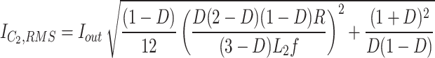
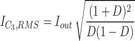
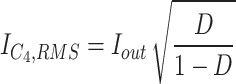
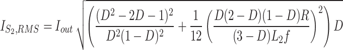
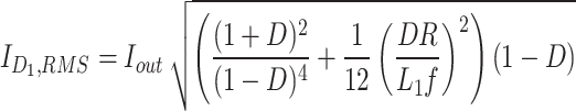
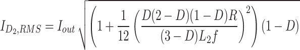
The root mean square (RMS) of devices’ current is necessary for performing the loss analysis. The equations of computing the RMS current of components’ currents have been presented in (Table 1).
Table 1.
RMS current of devices.
|
|

|
|
|
|

|
|
|
|

|

|
The average current of diodes is also calculated from (25). The total conduction loss of components is calculated through (26). The switching loss of switches is computed from (27), where ton/toff denotes the time for a switch to turn on/off.
 |
25 |
 |
26 |
 |
27 |
The efficiency of the converter can be calculated from (28).
 |
28 |
Comparisons
This section performs a comprehensive comparative analysis between the proposed topology and its similar counterparts presented in20–30, from viewpoints of: number of devices, number of operational modes in CCM (NM), maximum number of devices on current flow path (NCD), availability of common ground point (CG), continuity of input current (CIC), interleaved structure (IL), voltage gain (G), maximum voltage stress on switches and diodes (MVSS and MVSD), valid duty cycle range and efficiency at 300W load power. Table 2 presents the comparison results. Figures 8, 9 and 10 show the comparison results as plots to provide better understanding. Figure 8; Table 2 compares the number of required devices, operational modes and conducting devices in proposed converter (shown as P) and other counterparts. Also, to have fair comparisons, only similar topologies (non-isolated high-gain topologies) with hard-switching (like the proposed topology) have been selected for comparisons.20
Table 2.
Comparative analysis.
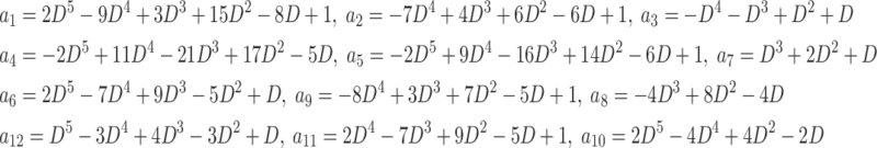
| Topology | Proposed | 20 | 21 | 22 | 23 | 24 | 25 | 26 | 27 | 28 | 29 | 30 |
|---|---|---|---|---|---|---|---|---|---|---|---|---|
| N S | 2 | 2 | 1 | 1 | 3 | 1 | 1 | 2 | 2 | 1 | 2 | 2 |
| N D | 4 | 5 | 4 | 5 | 3 | 5 | 5 | 2 | 2 | 4 | 4 | 4 |
| N C | 4 | 5 | 4 | 3 | 3 | 6 | 6 | 2 | 3 | 5 | 4 | 4 |
| N L | 2 | 2 | 1 | 3 | 3 | 2 | 4 | 2 | 3 | 2 | 2 | 2 |
| N T | 12 | 14 | 10 | 12 | 12 | 14 | 16 | 8 | 10 | 12 | 12 | 12 |
| N M | 2 | 2 | 2 | 2 | 2 | 2 | 2 | 4 | 2 | 2 | 2 | 2 |
| N CD | 3 | 5 | 4 | 6 | 6 | 6 | 7 | 3 | 5 | 5 | 5 | 4 |
| CG | Y | Y | N | Y | Y | Y | Y | Y | N | Y | N | Y |
| CIC | Y | Y | Y | Y | Y | Y | Y | Y | Y | Y | Y | Y |
| IL | Y | N | N | N | Y | N | N | Y | N | N | N | Y |
| G |

|

|

|

|

|

|
|

|

|

|

|

|
| G@D = 0.5 | 10 | 8 | 5 | 8 | 8 | 6 | 6 | 4 | 5 | 5 | 7 | 8 |
| D at G = 10 | 0.5 | 0.6 | 0.78 | 0.54 | 0.54 | 0.7 | 0.62 | 0.68 | 0.69 | 0.73 | 0.64 | 0.55 |
| MVSS |

|

|

|
V o | V o |

|

|
V o |

|

|

|

|
| MVSD |

|

|

|
V o |

|

|
|
V o |

|

|

|

|
| D range | [0–1] | [0–1] | [0–1] | [0–1] | [0–1] | [0–1] | [0–1] | [0-0.5] | [0–1] | [0–1] | [0–1] | [0–1] |
| η@300W | 95.5% | 96.1% | < 94% | < 89% | < 89% | 92.8% | 90.4% | 90% | < 90% | < 90% | 95% | 94.2% |
| Switching | Hard | Hard | Hard | Hard | Hard | Hard | Hard | Hard | Hard | Hard | Hard | Hard |
NS Number of switches, ND number of diodes, NC number of capacitors, NL number of inductors, NT number of total devices, NM number of modes in CCM, NCD number of devices on current flow-path, CG common-grounded, CIC continuous input current, IL interleaved structure, G gain, G@D = 0.5 gain at D = 0.5, MVSS maximum voltage stress on switches, MVSD maximum voltage stress on diodes, η@300W efficiency at 300W output power.
Fig. 8.

Number of devices, operational modes and maximum number of devices on current flow path in CCM.
Fig. 9.

(a) Gain vs. duty cycle during 0.05 ≤ D ≤ 0.55, (b) Gain vs. duty cycle during 0.55 ≤ D ≤ 0.95, (c) G/NT vs. duty cycle during 0.05 ≤ D ≤ 0.55, (d) G/NT vs. duty cycle during 0.55 ≤ D ≤ 0.95.
Fig. 10.

Duty cycle required for providing voltage gain of 10 (D at G = 10).
The proposed converters requires only two switches, which is equal or fewer than that of20,23,26,27,29,30. Also, the required diodes in proposed converter is equal or less than that of20–22,24,25,28–30. The proposed converter utilizes identical or fewer capacitors than20,21,24,25,28–30. The proposed converter requires only two inductors, which is the second least value among considered topologies. The synchronous operation of switches leads to only two operational modes in proposed topology and20–25,27–30, while the switches’ non-synchronous operation in26 leads to 4 operational modes, which complicates the control of converter. The proposed converter has the least maximum number of devices on current flow path, among considered converters. This property may lead to lower voltage drop and improved efficiency. The proposed converter and20,22–26,28,30 take the advantage of common ground point, which tackles the leakage current issue in PV applications, while the topologies presented in21,27,29 lack this important property. Furthermore, the proposed converter and all considered topologies benefit from continuous input current, which is very critical feature in PV, fuel-cell and battery applications. Moreover, among considered converters, the proposed converter along with the ones presented in23,26,30 are the only converters that profit from interleaved structure, which can lead to reduced losses at input-side devices and consequently to better total efficiency. Figure 9 shows the gain of proposed converter and other considered topologies versus different duty cycles. For clear view, separate plot has been provided for each of 0.05 ≤ D ≤ 0.55, and 0.55 ≤ D ≤ 0.95 sub-intervals. Based on Fig. 9, the proposed converter provides the highest gain across 0.33 ≤ D ≤ 0.57. Also, it yields the second highest gain across 0.05 ≤ D ≤ 0.33, and 0.57 ≤ D ≤ 0.95. Figure 9 confirms the high step-up capability of proposed converter at variety of (from low to high) duty cycles.
Based on Table 2, the voltage gain of proposed topology at duty cycle of 0.5 is equal to 10, which is higher than that of similar peers. This confirms high step-up capability of proposed topology. Figure 10 displays the required duty cycle for achieving the gain of 10. According to Table 2; Fig. 10, the proposed converter can achieve a voltage gain of 10 with mild duty cycle of 0.5, which is the least value among considered converters. Figure 11a, b respectively shows the maximum voltage stress (in per unit) on switches and diodes, versus different duty cycles. As seen from Fig. 11, the maximum voltage stress on semiconductors of proposed converter is less than the output voltage (less than 1 P.U.). Thus, the low-rated semiconductors with low on-state resistance can be employed. According to Fig. 11, the maximum voltage stress on semiconductors of22,23,26 is equal to the output voltage. It is also seen from Fig. 11b that the maximum voltage stress on diodes of27 is even higher than the Vo at D ≤ 0.34.
Fig. 11.

Maximum voltage stress on (a) Switches (MVSS), (b) Diodes (MVSD), versus duty cycle.
According to Table 2, the valid duty cycle range of26 is narrow and limited to 0.5, while the proposed converter and other topologies have wide duty cycle range, from zero to unity. As the last factor, the efficiency of proposed and other considered converters has been compared at output power of 300W. Based on Table 2, the proposed converter provides the second highest efficiency among considered converters. Also, according to Table 2, the proposed and selected topologies use hard switching.
Experimental analysis
In this section, experimental analysis is performed on laboratory-scaled (350W) prototype of proposed converter to validate its appropriate performance, as shown in (Fig. 12). Also, Table 3 shows the parameters’ values used in experimental analysis.
Fig. 12.

Implemented prototype of proposed converter.
Table 3.
Parameters/devices values/models used in experimental analysis.
| Parameter/devices | Value/model |
|---|---|
| Input voltage (Vin) | 48V |
| Duty cycle (D) | 30% |
| Output voltage (Vout) | 245V |
| Output power (Pout) | 350W |
| Load current (Io) | 1.45A |
| Switching frequency (f) | 31kHz |
| Load (R) | 167Ω |
| L1, L2 inductors | 800µH, 1.1mH |
| C1, C2, C3, C4 Capacitors | 100µF, 220µF, 100µF, 220µF |
| Switches | IRFP260N MOSFETs |
| Diodes | MUR1560 |
| Microcontroller | Arduino Uno R3 |
Figure 13 displays the input/output voltage/current waveforms. As seen from Fig. 13a, the experimental results obtained load voltage and current are respectively about 245V and 1.45A, at steady-state condition. Thus, the load power is about 350W. The difference between the experimental (245V) and theoretical (264V) values is due to the losses occurred on parasitic elements of devices. The experimentally achieved voltage gain at low duty cycle of 30% is about 5, which is quite high. Also, according to Fig. 13b, the input voltage is 48 V, where the average of input current is about 8A. The source current is continuous with ripple of about 2A. It is kindly stated that the experimental analysis has been conducted at D = 0.3 to show the high step-up capability of the proposed topology even at very low duty cycles. Producing a voltage gain of 5 at low duty cycle of D = 0.3 confirms the high step-up capability of the proposed topology. According to Fig. 9a, b, the gain of proposed topology at higher duty cycles is considerable and higher than that of its peers.
Fig. 13.

Experimental results for (a) output (load), (b) input.
(source), voltage and current waveforms.
Figure 14 shows the inductors’ voltage/current waveforms. As seen, the proposed converter operates in CCM, where the average current values of L1-L2 inductors are respectively about 4A and 4.28A. The current ripple of L1-L2 inductors have also been limited to about 0.8A and 1A, respectively.
Fig. 14.

Experimental results for voltage/current waveforms of (a) L1, (b) L2, inductors.
The voltage and current waveforms of capacitors have been shown in (Fig. 15). As seen, the voltage of C1-C4 capacitors has been regulated respectively on 64V, 92V, 146V and 146V, which are confirmed by theoretical values obtained from (3).
Fig. 15.

Experimentally obtained results for voltage/current waveforms of (a) C1, (b) C2, (c) C3, (d) C4, capacitors.
Figure 16 displays the voltage/current stress of switches. According to Fig. 16, the voltage stress of S1-S2 switches are respectively about 63V (0.26Vo), and 90V (0.37Vo), which are much less than Vo. Also, the current stress of S1-S2 switches are respectively about 14A and 9A. The experimental results obtained for voltage and current stress of switches are validated by (5) and (9).
Fig. 16.

Experimentally obtained results for voltage/current waveforms of (a) S1, (b) S2, switches employing snubber.
Figure 17 illustrates the diodes’ voltage/current waveforms. It is seen that the voltage stress of D1-D4 diodes are respectively about 63V (0.26Vo), 143V (0.58Vo), 143V (0.58Vo), and 143V (0.58Vo), all of which are less than Vo. The current stress of D1-D4 diodes are also equal to 4A, 3A, 6A, and 2.8A, respectively. The achieved results are confirmed by (5) and (9).
Fig. 17.

Experimentally obtained results for voltage/current waveforms of (a) D1, (b) D2, (c) D3, (d) D4, diodes.
Figure 18a shows the experimentally measured and theoretically calculated efficiencies of proposed topology. The theoretical efficiency is calculated from theoretical and simulation-based analysis, where the simulation analysis is responsible for providing the root mean square (RMS) and average current values of devices, where the real model of components is used to resemble the real condition. The devices’ RMS and average current values (obtained from simulations) are used in theoretical analysis to compute the components’ losses and converter’s efficiency. As seen, the peak efficiency of the proposed topology (similar to its non-isolated high step-up peers) occurs at low output powers. As the power increases, the efficiency decreases. The experimentally measured and theoretically estimated efficiency of the proposed topology at Pout=350W are respectively about 97.1 and 95.7%. Figure 18b shows the power loss distribution between the devices of proposed converter at Po=350W (Vin=48V, D = 30%, R = 167Ω). As seen, the highest portion (6.26W, 41%) of losses belongs to the diodes, where the capacitors have the least portion (0.3W, 2%). The total power loss of proposed converter at this operating point (Pout=350W) is about 15.28W, which provides a theoretically estimated efficiency of about 95.7%.
Fig. 18.

(a) Efficiency curve of proposed converter vs. output power, (b) loss distribution between devices at Pout=350W.
Dynamic modeling analysis
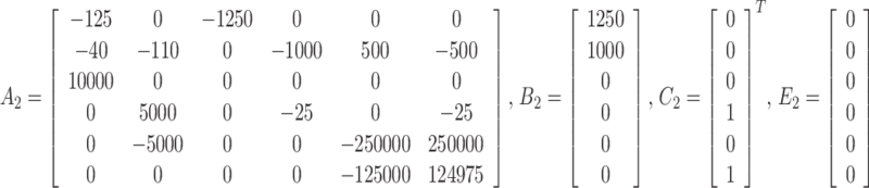
In this section, the state space averaging method and small-signal analysis are employed to model the proposed topology and investigate its operation during dynamic conditions.
Small-signal model of the proposed converter
The goal of this sub-section is to derive the proposed topology’s state space average model and its control-to-output voltage transfer function (Gvd). During mode 1, the proposed topology’s state space equations are as shown in (29), (30).
 |
29 |
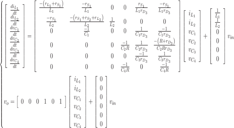 |
30 |
The parameters used in the modeling process have been listed in (Table 4). To simplify the modeling process, the equivalent series resistance of capacitors along with the forward voltage drop of diodes have been neglected.
Table 4.
Parameters used during small-signal modeling of the proposed topology.
| Parameter | Definition | Parameter | Definition | Parameter | Definition |
|---|---|---|---|---|---|
| L 1 | L1 Inductance value |

|
Resistance of on-state switch S1 | R | Load resistance |
| L 2 | L2 Inductance value |

|
Resistance of winding for inductor L1 | D | Large value of duty cycle |
| C 1 | C1 Capacitance value |

|
Resistance of winding for inductor L2 |

|
Small value of duty cycle for control input |
| C 2 | C2 Capacitance value |

|
Resistance of on-state diode D1 | v in | Small signal input voltage |
| C 3 | C3 Capacitance value |

|
Resistance of on-state diode D2 | v out | Small signal output voltage |
| C 4 | C4 Capacitance value |

|
Resistance of on-state diode D3 | x | State variable vector |

|
Resistance of on-state switch S1 |

|
Resistance of on-state diode D4 | y | Output vector |
In mode 2, the proposed topology’s state space equations are as shown in (31)-32).
 |
31 |
 |
32 |
The average state space equations can be achieved as (33).
 |
33 |
The control-to-output voltage transfer function (Gvd) of proposed topology can be obtained as (34), where X can be computed from (35).
 |
34 |
 |
35 |
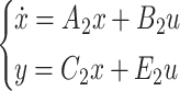
Using parameters’ values shown in (36), the A1, A2, A, B1, B2, B, C1, C2, C, E1, E2, and E matrixes are obtained from (37)-(39).
 |
36 |
 |
37 |
 |
38 |
 |
39 |
Accordingly, the control-to-output voltage transfer function (Gvd) of proposed topology can be calculated from (40).
 |
40 |
The bode diagrams of average state-space model (Gvd transfer function) of proposed converter are shown in (Fig. 19). As seen, the proposed converter is stable, but has a large phase margin, which may slow down the system dynamic response.
Fig. 19.

Bode diagrams of proposed converter’s transfer function.
Simulation results for closed-loop control
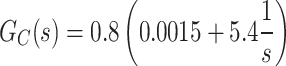
Figure 20 shows the schematic of applied closed-loop control system, which is consisted of a PI controller, carrier signal, comparator, voltage sensor and subtractor for producing error signal. The duty cycle is considered as the control input signal and the output voltage (Vout) is considered as the system response, where the changes in input voltage and load resistance are considered as the disturbances. The goal of closed-loop control system is to track the reference signal and eliminate the effects of disturbances in a sufficiently short period of time. The Proportional-Integral (PI) controller and its parameters have been designed based on the average state-space model of the proposed converter. The transfer function of designed PI controller (GC) is shown in (41).
 |
41 |
Fig. 20.

Block diagram of closed-loop control system.
The designed closed-loop control system has been implemented on the proposed converter and has been simulated in PSCAD/EMTDC software, using the parameter values presented in (Table 3). Figure 21 investigates the dynamic behavior of closed-loop control system during sudden step changes in either of output voltage reference value (Fig. 21a), input voltage (Fig. 21b) and load resistance (Fig. 21c). In Fig. 21a, the output voltage reference value suddenly increases from 245 to 285V at t = 0.3 Sec and return to 245[V] as a step-change at t = 0.5 Sec. According to Fig. 21a, the output voltage generated by the closed-loop control system effectively tracks the reference value with sufficiently short transient period (less than 0.1 Sec). Figure 21b, c display the response of closed-loop control system against disturbances in input voltage and load resistance. In Fig. 21b, the input voltage experiences an increasing step-change from 48 to 55V at t = 0.3 Sec and a decreasing step-change from 55 to 48V at t = 0.5 Sec. As observed from Fig. 21b, the output voltage does not experience considerable change during step-changes in input voltage. Moreover, the response of closed-loop control system to sudden load change (from 167 to 200Ω at t = 0.3 Sec and from 200 to 167Ω at t = 0.5 Sec) is shown in (Fig. 21c). Here again, the effect of sudden load changes on the output voltage has been successfully cancelled by the employed closed-loop control system. These results confirm the good performance of the proposed converter and its closed-loop control system during dynamic conditions, including the elimination of effect of disturbances on the output voltage.
Fig. 21.

Performance of closed-loop control system during step-changes in, (a) Output voltage reference value (VRef), (b) input voltage, (c) load resistance.
Conclusion
In this paper, a dual-switch switched-capacitor based DC-DC converter has been proposed that benefits from features like: (1) high step-up capability even at mild duty cycles, (2) availability of common-ground point, which tackles the leakage current issue at PV applications, (3) low voltage stress on switching devices, (4) wide duty cycle range, (5) large ratio of voltage gain per number of devices, (6) minimum (only 2) operational modes, which eases the modeling and control of the converter, (7) continuous source current, (8) interleaved structure, which leads to reduced losses at input-side devices. The proposed converter has been introduced and its operation during both CCM and DCM modes has been investigated in detail. The steady-state analysis as well as real-gain calculations and components’ design procedure have also been provided. The superiority of proposed converter over similar counterparts have been certified by comprehensive comparative analysis. Based on comparison results, the proposed converter provides higher ratio of gain per devices than other counter parts. A laboratory-scaled 350W prototype of proposed converter has been implemented with input voltage of 48V, switching frequency of 31kHz, and duty cycle of 30%. The experimental analysis shows a gain of about 5 at low duty cycle of D = 0.3, which is considerable for such a low duty cycle. The efficiency of implemented 350W prototype is about 95%, which is reasonable. The experimentally obtained results are in a good accordance with the presented theoretical analysis, which confirms the correct operation of proposed converter. Furthermore, the appropriate dynamic operation of proposed converter has been verified through simulation analysis.
Acknowledgements
This work is based upon research funded by Iran National Science Foundation (INSF) under project No.4004592.
Author contributions
Conceptualization, A.G.E. and K.V.; methodology, A.G.E. and K.V.; software, A.G.E. and K.V.; validation, A.G.E., and K.V.; investigation, A.G.E., and K.V.; resources, A.G.E., and K.V.; data curation, A.G.E., and K.V.; writing—original draft preparation, A.G.E., and K.V.; supervision, K.V.; Funding acquisition: K.V.; Visualization: K.V.; writing—review and editing: K.V., and A.G.E.; project administration, K.V.; Formal analysis: A.G.E., and K.V., All authors have read and agreed to the published version of the manuscript.
Data availability
The datasets used and/or analyzed during the current study available from the corresponding author on reasonable request.
Declarations
Competing interests
The authors declare no competing interests.
Footnotes
Publisher’s note
Springer Nature remains neutral with regard to jurisdictional claims in published maps and institutional affiliations.
References
- 1.Nouri, T., Hasanpour, S. & Lee, S. S. A semi-quadratic trans-inverse high step-Up DC-DC converter for renewable energy applications. IEEE Trans. Power Electron., (2024).
- 2.Valarmathy, A. & Prabhakar, M. Non-isolated high gain DC–DC converter with ripple-free source current. Sci. Rep.14 (1), 973 (2024). [DOI] [PMC free article] [PubMed] [Google Scholar]
- 3.Esfahlan, A. G. & Varesi, K. A quasi Z-source (QZS) network-based quadratic boost converter suitable for photovoltaic-based DC microgrids, DC microgrids: advances, challenges, and applications, 325–360, (2022).
- 4.Hasanpour, S. & Lee, S. S. A new quadratic DC/DC converter with ultra-high voltage gain. IEEE Trans. Power Electron. (2024).
- 5.Varesi, K., Hassanpour, N. & Saeidabadi, S. Novel high step-up DC-DC converter with increased voltage gain per devices and continuous input current suitable for DC microgrid applications. Int. J. Circuit Theory Appl.48 (10), 1820–1837 (2020). [Google Scholar]
- 6.Alhurayyis, I., Elkhateb, A. & Morrow, J. Isolated and nonisolated DC-to-DC converters for medium-voltage DC networks: a review. IEEE J. Emerg. Sel. Top. Power Electron.9 (6), 7486–7500 (2020). [Google Scholar]
- 7.Forouzesh, M., Siwakoti, Y. P., Gorji, S. A., Blaabjerg, F. & Lehman, B. Step-up DC-DC converters: a comprehensive review of voltage-boosting techniques, topologies, and applications. IEEE Trans. Power Electron.32 (12), 9143–9178 (2017). [Google Scholar]
- 8.Tarzamni, H., Gohari, H. S., Sabahi, M. & Kyyrä, J. Nonisolated high step-up DC–DC converters: comparative review and metrics applicability. IEEE Trans. Power Electron.39 (1), 582–625 (2023). [Google Scholar]
- 9.Bhaskar, M. S. et al. Survey of DC-DC non-isolated topologies for unidirectional power flow in fuel cell vehicles. IEEE Access8, 178130–178166 (2020). [Google Scholar]
- 10.Eslamloo, M. K., Varesi, K., Tarzamni, H. & Lee, S. S. Comprehensive reliability review and assessment of switched-capacitor step-up DC-DC converters. IEEE Trans. Reliab. (2024).
- 11.Malick, I. H., Zaid, M., Ahmad, J., Varesi, K. & Lin, C. H. Implementation and reliability analysis of a new non-isolated quadratic buck-boost converter using improved Markov modelling. IET Renew. Power Gener.17 (11), 2733–2749 (2023). [Google Scholar]
- 12.Reddy, A. B., Mahato, S. & Tewari, N. Dual switch ultra-high gain DC-DC converter with low voltage stress. AEU-International J. Electron. Commun.173, 154995 (2024). [Google Scholar]
- 13.Marzang, V. et al. A high step-up nonisolated DC–DC converter with flexible voltage gain. IEEE Trans. Power Electron.35 (10), 10489–10500 (2020). [Google Scholar]
- 14.Gu, Y., Chen, Y., Zhang, B., Qiu, D. & Xie, F. High step-up DC-DC converter with active switched LC-network for photovoltaic systems. IEEE Trans. Energy Convers.34 (1), 321–329 (2018). [Google Scholar]
- 15.Gopinathan, S., Rao, V. S. & Sundaramoorthy, K. Family of non-isolated quadratic high gain DC-DC converters based on extended capacitor-diode network for renewable energy source integration. IEEE J. Emerg. Sel. Top. Power Electron.10 (5), 6218–6230 (2022). [Google Scholar]
- 16.Rahimi, R., Habibi, S., Ferdowsi, M. & Shamsi, P. Z-source-based high step-up DC-DC converters for photovoltaic applications. IEEE J. Emerg. Sel. Top. Power Electron.10 (4), 4783–4796 (2021). [Google Scholar]
- 17.Singh, A. et al. Quasi-impedance-source-network-based nonisolated high-step-up DC-DC converter. IEEE Trans. Ind. Appl.57 (6), 6405–6416 (2021). [Google Scholar]
- 18.Zhang, G. et al. A generalized additional voltage pumping solution for high-step-up converters. IEEE Trans. Power Electron.34 (7), 6456–6467 (2018). [Google Scholar]
- 19.Maalandish, M., Hosseini, S. H., Ghasemzadeh, S., Babaei, E. & Jalilzadeh, T. A novel multiphase high step-up DC/DC boost converter with lower losses on semiconductors. IEEE J. Emerg. Sel. Top. Power Electron.7 (1), 541–554 (2018). [Google Scholar]
- 20.Mohammed, M. R., Al-Sumaiti, A. S., Beig, A. R., Al Hosani, K. & Wang, C. A common grounded voltage quadrupler ASL/PSC hybrid converter with reduced voltage stress. IEEE Trans. Industr. Electron.71 (5), 4773–4784 (2023). [Google Scholar]
- 21.Mohammadi, F., Gharehpetian, G. B., Rastegar, H. & Farhadi-Kangarlu, M. Non-isolated step-up DC-DC converter based on switched capacitor cells. CSEE J. Power Energy Syst.9, 3, (2023).
- 22.Kumar, G. G., Krishna, M. S., Kumaravel, S. & Babaei, E. Multi-stage DC-DC converter using active LC2D network with minimum component. IEEE Trans. Circuits Syst. II Express Briefs68 (3), 943–947 (2020). [Google Scholar]
- 23.Varesi, K. & Padmanaban, S. A transformer-less high-boosting common-grounded multi-phase DC-DC Converter with Continuous input-current Favourable for low-power Applications (IET Renewable Power Generation, 2022).
- 24.Alilou, S. M. et al. A new high step-up DC-DC converter using voltage lift techniques suitable for renewable applications. CSEE J. Power Energy Syst. (2023).
- 25.Rajesh, R., Prabaharan, N. & Santhosh, T. Design and analysis of a non-isolated DC-DC converter with a high-voltage conversion ratio. IEEE Trans. Circuits Syst. II Express Briefs70 (6), 2036–2041 (2022). [Google Scholar]
- 26.Bussa, V. K., Singh, R. K., Mahanty, R. & Lal, V. N. Design and analysis of step-up interleaved DC-DC converter for different duty regions. IEEE Trans. Ind. Appl.56 (2), 2031–2047 (2020). [Google Scholar]
- 27.Selvam, S., Sannasy, M. & Sridharan, M. Analysis and design of two-switch enhanced gain SEPIC converter. IEEE Trans. Ind. Appl.59 (3), 3552–3561 (2023). [Google Scholar]
- 28.Asgarnia, R. & Afjei, E. A novel high-efficient step-up converter with continuous input current, common ground, and minimum stress on semiconductors. IET Power Electron.16 (7), 1128–1145 (2023). [Google Scholar]
- 29.Cui, C., Tang, Y., Guo, Y., Sun, H. & Jiang, L. High step-up switched-capacitor active switched-inductor converter with self-voltage balancing and low stress. IEEE Trans. Industr. Electron.69 (10), 10112–10128 (2021). [Google Scholar]
- 30.Li, Z., Liu, J., Yang, N., Ying, G. & Zeng, J. Dual-working-modes-based common grounded nonisolated DC-DC converter with a wide voltage-gain range for photovoltaic applications. IEEE Trans. Energy Convers. (2023).
- 31.Kazimierczuk, M. K. Pulse-width Modulated DC-DC Power Converters (Wiley, 2015).
- 32.Varesi, K. et al. Design and analysis of a developed multiport high step-up DC–DC converter with reduced device count and normalized peak inverse voltage on the switches/diodes. IEEE Trans. Power Electron.34 (6), 5464–5475 (2018). [Google Scholar]
- 33.Valarmathy, A., Prabhakar, M. & Varesi, K. Non-isolated high gain DC-DC converter for PV-fed DC microgrid. Int. J. Sustain. Eng.17 (1), 32–50 (2024). [Google Scholar]
Associated Data
This section collects any data citations, data availability statements, or supplementary materials included in this article.
Data Availability Statement
The datasets used and/or analyzed during the current study available from the corresponding author on reasonable request.