

Abstract

Janus monolayers are two-dimensional materials with distinct chemical compositions on their opposing sides, leading to unique properties and potential applications in various fields. Based on density functional theory (DFT) calculations, we have explored the dynamic stability of a family of Janus monolayers with the general formula TMCSe (TM = Sc, Ti, V, Cr, Mn, Fe, Co, Ni, Cu, Zn). Only two explored systems were dynamically and thermal stable: CrCSe and MnCSe, as evidenced by their phonon dispersion curves and molecular dynamics calculations. Their electronic properties and magnetic character have been investigated using their corresponding density of states. The CrCSe monolayer is a 0.4 eV indirect semiconductor, and the magnetic MnCSe monolayer is spin-up metallic and a spin-down semimetal. Electrostatic potential isosurfaces are used to assess the reactivity of the stable monolayers. They indicate that the surfaces of the TMCSe structures are polarized, with the C side exhibiting a strong negative potential and the Se side displaying a more neutral character. This property may lead to applications in many fields, such as Li storage or toxic molecule trapping.
1. Introduction
Since the discovery of graphene by Geim and Novoselov in 2004,1 interest in two-dimensional (2D) materials has increased. Different research groups have worked to find new 2D materials with properties comparable to those of graphene. Examples include silicene,2 germanene,3 transition metal dichalcogenides (TMD),4−6 and Janus monolayers.7 2D transition metal dichalcogenides (TMDs) have gained attention due to their unique physical and chemical properties as they transition from multilayers to monolayers. Notable features include the shift from an indirect to a direct band gap,8 significant excitonic binding energy,9 and the abundance of multiexcitons.10 Most TMD monolayers have band gaps in the 1–3 eV range, facilitating the emergence of advanced nanodevices.11−13 The presence of an intrinsic direct band gap and the unique electronic and optical properties of 2D TMD monolayers14 make them versatile materials for diverse applications as catalysts,15 transistors,16 components in batteries,17,18 and optoelectric applications.19−22 TMDs appear in two main phases: honeycomb structures (1H)23 (a single layer of the 2H multilayer bulk phase) and centered honeycomb structures (1T).24 The structural composition of 2D monolayer transition metal dichalcogenides (TMDs) is characterized by a sandwich-like arrangement comprising a double layer of chalcogen atoms (each on opposing sides) enclosing the transition metal atom. Typically, the chalcogen atoms on both sides correspond to the same chemical element. However, when the chalcogen atoms in the two layers differ, they form a 2D structure known as Janus transition metal dichalcogenide monolayers (JTMDs). These novel materials exhibit asymmetric structures and have garnered considerable attention as a distinct class of 2D semiconductors. Their structural properties render them particularly intriguing for various applications in energy conversion technology,25 quantum science,26 and the burgeoning field of spintronics.27 A methodology for synthesizing JTMD capable of disrupting the out-of-plane structural symmetry has been detailed in ref (28). Furthermore, controlled sulfuration has been employed to synthesize a two-dimensional monolayer with an asymmetric structure known as MoSSe.29 Investigation into the Janus MoSSe monolayer has revealed compelling properties for the detection of SO2, SO2F2, H2S, SOF2, and primarily SOF6, showcasing its potential utility in gas-insulated switches (GIS) and the fabrication of ultrahigh sensitivity nanodevices.30 Recent studies have also delved into areas such as band gap engineering,31 solar water splitting,32,33 and photocurrent response,34 focusing on the Janus MoSSe monolayer. Additionally, the Janus PtSSe monolayer has been identified for its advantageous properties as a promising photocatalyst, leveraging its internal electric field to facilitate the hydrogen evolution reaction.35 Further investigations have been conducted on additional 2D Janus materials, including Janus MXenes36 and Janus chalcogenide monolayers of group III.37 The band gap of Janus MXenes can be adjusted by selecting a suitable pair of chemical elements to terminate the surfaces and bottom layers of the MXenes.36 Janus group-III chalcogenide monolayers exhibit higher piezoelectric coefficients compared to their pristine counterparts.37 The unique physical properties of these novel 2D systems, coupled with the successful synthesis of Janus MoSSe monolayers, suggest the potential utility of 2D JTMDs in nanoscale devices for electronic and energy applications.26 This study examines a series of Janus TMCSe (TM= Sc, Ti, V, Cr, Mn, Fe, Co, Ni, Cu, Zn) built by a triple single-layer with a TM atom enclosed by C and Se atoms at the opposite faces of the monolayer to explore their dynamic stability and electronic properties further. The C atomic layer was chosen due to its abundance and to explore the difference in electronegativity on the opposite faces of this material. Such a feature is less evident in Janus structures formed by purely chalcogen elements, and the possibility of having a highly polarized surface is desirable for applications in photocatalysis and electronic devices, such as transistors, where asymmetric charge distribution is desirable.38−40 This investigation uses first-principles calculations based on density functional theory (DFT). The insights gained from these analyses will inform the future utilization of these monolayers in nanoscale devices.
2. Materials and Methods
Spin-polarized total energy calculations within the density functional theory framework as implemented in the Quantum ESPRESSO package41 have been conducted to explore the stability of the proposed systems. The Kohn–Sham states were expanded using a plane wave basis set with a kinetic energy cutoff of 75 Ry and a charge density expansion of 600 Ry. Exchange-correlation energies were treated within the generalized gradient approximation (GGA), employing the Perdew–Burke–Ernzerhof (PBE) functional.42 Electron–ion interactions were handled with ultrasoft pseudopotentials.43 For Brillouin zone integration,44 we have used a Monkhorst–Pack mesh with gamma-centered k-point grids of 8 × 8 × 1 to optimize the Janus layers and 16 × 16 × 1 to calculate electronic properties. An energy convergence criterion was set to 10–6 eV. Geometric structures were optimized by minimizing the forces on individual atoms with a convergence criterion requiring all forces on each atom to be smaller than 1 × 10⁻³ Ry/a.u. A vacuum size of 15 Å in the z-direction was utilized to prevent self-interactions due to the Born-von Karman boundary conditions.
3. Results and Discussion
3.1. Structural Properties
To determine the ground state energy of the designed TMCSe monolayers (TM= Sc, Ti, V, Cr, Mn, Fe, Co, Ni, Cu, Zn) through first-principles calculations based on DFT, we started our analysis by conducting a relaxation of the atomic structures by minimizing the Hellmann–Feynman forces46 to optimize the lattice constant of the unit cells. However, among all the combinations explored, only three structures exhibited mostly positive phonon scattering bands (see section 3.3). Consequently, in this work, we focus solely on the stable structures CrCSe, MnCSe, and NiCSe (all phonon dispersions are shown in S.I.). Each model possesses a trigonal crystal system (see Figure 1) and belongs to the P3m1 space group.47 The optimized lattice constant of the unit cells was determined by identifying the minimum of the Energy-Volume curve. The lattice constants, bond lengths, and bond angles obtained are shown in Table 1.
Figure 1.

(a) Top view of the Janus TMCSe (TM= Cr, Mn, Ni) monolayer, (b) side view. The continuous red line encloses the unit cell. We used the VESTA45 program.
Table 1. Optimized Lattice Parameter a, Bond Length, and Bond Angle of the 2D Janus Layers.
| lattice parameter (Å) | bond
length (Å) |
bond angles (deg) | ||
|---|---|---|---|---|
| layer | a = b | dSe–TM | dTM–C | Se–TM–C |
| CrCSe | 3.06 | 2.5 | 1.91 | 86.7 |
| MnCSe | 3.03 | 2.6 | 1.87 | 87.3 |
| NiCSe | 3.25 | 2.4 | 1.93 | 77.1 |
3.2. Charge Distribution
Motivated by the differences in bond lengths, we examined the variations in bond character associated with each TM and their interaction with C and Se atoms on opposite faces. Figure 2 illustrates a plane projection area that intersects the system and shows the charge distribution regions for the bonds present. An RGB color code differentiates between regions of zero, low, and high charge. The lower part of the figure depicts planes for each system; it can be observed that the TM-C bond on the upper face is consistently characterized by a red color across all models, indicating its strength. In contrast, TM-Se bonds on the lower face are weaker, as denoted by low charge overlap regions, indicating directional anisotropic properties. Note that the TM-Se bond charge distribution is more uniform for Cr and Ni, while Mn exhibits a more localized nature.
Figure 2.

Charge distribution region of Janus TMCSe in (a,b) CrCSe, (c,d) MnCSe, and (e,f) NiCSe. An RGB color code was employed to differentiate charge concentration regions, where blue indicates zero charge and red represents high charge concentration values.
3.3. Dynamic Stability
To assess the dynamical stability of the predicted 2D materials, we used the Quantum ESPRESSO code to calculate the phonon dispersion path along the high-symmetry points Γ, K, and M (see Figure 3). The phonon dispersion diagram of each system is composed of nine phonon modes, as the unit cell of the TMCSe monolayers consists of three atoms. The three lower branches correspond to the acoustic phonon modes, while the six upper branches represent the optical phonon modes. Note that for CrCSe and MnCSe(Figure 3(a,b)), a soft crossing between an acoustic and an optical branch is observed, suggesting that the bonds could be prone to geometrical distortions.48 The figure illustrates a mode with a small region with small negative values (−4 cm–1 at the Γ point) for CrCSe, and for NiCSe (−16 cm–1 at the Γ point) for NiCse. A similar situation has been reported for buckled germanene,49 and arsenene,50 and it has been attributed to the softening of phonons. As shown in a following section, molecular dynamics simulations show that CrCSe is stable, but NiCSe is not. On the other hand, no imaginary mode is detected for MnCSe. The absence of significant negative modes in the phonon branches across the Brillouin zone implies that all three predicted monolayers are kinetically stable.
Figure 3.

Phonon dispersion analysis of the fully optimized transition metal chalcogenide Janus monolayers: (a) CrCSe, (b) MnCSe, and (c) NiCSe.
3.4. Electronic Properties
Complementary to the structural characterization, we investigated the electronic properties of the proposed TMCSe monolayers by analyzing their spin-resolved band structures and density of states. The calculated spin-resolved band structures of the TMCSe compounds are displayed in Figure 4. The bands are projected along the path of the high-symmetry points Γ-(0,0,0)-K-(0.5,0,0)-M-(0.5,0.5,0)-Γ-(0,0,0) to map the first Brillouin zone. The band dispersion indicates that the CrCSe monolayer is a nonmagnetic indirect semiconductor with a band gap of approximately 0.4 eV (see Figure 4(a)). The valence band maximum (VBM) is located at the Γ point, while the conduction band minimum (CBM) is between the K and Γ points. The density of states confirms the structure’s semiconducting nature, as there is an absence of states near the Fermi level. The most significant contribution near the Fermi level comes from Cr atoms, whereas C and Se atoms make relatively small contributions compared to Cr. The magnetic MnCSe monolayer presents an intriguing scenario (see Figure 4(b)). The spin-up configuration, exhibits a magnetic metallic behavior; the conduction band crosses the Fermi level at the K point, the VBM is located at the Γ point, and the CBM is positioned between the K and M points. The density of states confirms the metallic nature of the spin-up state of MnCSe, since there is a significant signal near the Fermi level, with the Se making the most significant contribution around the Fermi level, where Mn and C have minimal contributions. In the spin-down configuration, MnCSe also lacks a gap, showing a magnetic semimetal behavior. The VBM is at the Γ point, while the CBM is between the M and Γ points. The density of states confirms the metallic nature of the material, with Mn making the most significant contribution around the Fermi level, whereas C and Se have minimal contributions. Finally, the NiCSe monolayer exhibits a nonmagnetic metallic behavior, as depicted in Figure 4(c). The valence and conduction bands intersect near the Fermi level, with the VBM located at the Γ point and the CBM positioned between points K and Γ. The density of states confirms the structure’s metallic nature, as there is a significant signal near the Fermi level. The largest contribution near the Fermi level comes from C, although we observe similar contributions from all three elements are observed at negative energies.
Figure 4.

Electronic band structures (black line: spin-unpolarized; red line: spin-up; blue line: spin-down) and density of states of TMCSe. The dashed line denotes the Fermi level, set to zero.
A PDOS analysis was also performed; in Figure 5, similar signals can be seen near the Fermi level between the d orbital of Cr and the p orbital of C. This indicates hybridization between the atoms. In addition, near 1 eV, a very similar signal is observed between the p orbital of C and the p orbital of Se, thus confirming a hybridization between these atomic species. In Figure 6, a hybridization between the d orbitals of Mn, the p orbital of C, and the p orbital of Se is observed near the Fermi level for the Up state of MnCSe at 1 eV. In the case of C, the s orbital also appears to contribute. Finally, in Figure 7, it is observed that all three atomic species contribute to the metallic state of the monolayer. Hybridization is also seen between the d orbital of Ni, the p orbital of C, and the p orbital of Se near the Fermi level. We observe that there is interaction between atomic species of the three monolayers, which also shows that there is a bond between the atoms.
Figure 5.

DOS and PDOS of the CrCSe. The dashed line denotes the Fermi level, set to zero.
Figure 6.

DOS and PDOS of the MnCSe. The dashed line denotes the Fermi level, set to zero.
Figure 7.

DOS and PDOS of the NiCSe. The dashed line denotes the Fermi level, set to zero.
The band gap was also recalculated for the semiconductor structure CrCSe using the HSE06 functional. Figure 8 shows an increased band gap of 0.9 eV obtained with this approach compared to the 0.4 eV value obtained with a PBE functional. For the MnCSe and NiCSe monolayers, the HSE06 functional was not employed since the band structure of both systems displays a metallic character with the PBE functional.
Figure 8.
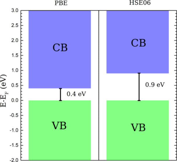
Estimated band gap of the CrCSe monolayer using HSE06 and PBE potentials. The green and blue bars represent VBM and CBM positions, respectively.
3.5. Bader Charge Analysis
In this section, we conducted a Bader charge (BC) analysis to investigate the charge transfer and redistribution between the atoms within the TMCSe monolayers. The BC formalism quantifies charge distribution values by atom.51 The analysis of charge distribution (ΔQ = evalence – BC) in a system can offer valuable insights into electron transfer between atoms, which consequently influences the material’s chemical and electrical properties. Table 2 summarizes the information on the calculated ΔQ and bond length values for each system. Our findings reveal that in all three Janus layers, the transition metal acts as an electron donor to the neighboring atoms on the faces of the monolayer, resulting in a positive charge at the center of the sheet and a negative charge on the surface.
Table 2. Bader Charge Analysis of the Three Layers.
| Layer | Atom | ΔQ(e) |
|---|---|---|
| CrCSe | Cr | 1.23 |
| C | –0.88 | |
| Se | –0.34 | |
| MnCSe | Mn | 1.07 |
| C | –0.77 | |
| Se | –0.28 | |
| NiCSe | Ni | 0.55 |
| C | –0.44 | |
| Se | –0.11 |
Notably, in the case of CrCSe, the Cr atom donates more electrons than other transition metals in their respective Janus layers. This observation suggests a stronger interaction between chromium, carbon, and selenium atoms, as indicated in Section 3.2. The BC values help identify the charge transfer mechanism. The fractional values obtained do not correspond to the actual oxidation states of the elements but provide a measure of the charge transfer to and from the atoms
In the system configuration, the TM atoms are located in the interlayer, which is six-fold coordinated, with three C and three Se atoms, resulting in octahedral coordination. In this configuration, crystal field theory for d orbitals predicts that the degeneracy of these orbitals is lifted due to the electrostatic interaction between the metal ion and its surrounding ligands. This interaction leads to different energy levels for the five d orbitals, causing a distortion in their spatial distribution within the crystal field and forming two band groups: the low-energy t2g and the high-energy eg bands. Table 2 shows the orbital occupation of the d orbitals for the transition metal atom in the interlayer configuration.
3.6. Electrostatic Potential Isosurface
In this section, we analyze the electrostatic potential isosurfaces (EPI) of the TMCSe to identify regions with charge concentrations in real space. These maps offer insights into the distribution of electrostatic charges within the structures, using an RGB color code to represent charge concentration in red and charge depletion in blue. The EPI is depicted using a 0.05 au isovalue. Figure 9 illustrates the EPI of the TMCSe structure. A top view of both faces reveals that the surface exhibits a highly negative potential on the carbon side. Therefore, the C side should show a preferential affinity for molecules with positive potentials. Note that this tendency is maintained for Cr and Mn (see Figure 9(a,c)). However, the C atoms of the Ni system present a less polar character (see Figure 9(e)). Conversely, the Se side of the surfaces displays a green coloring associated with low charge depletion values. The coloring is maintained for Cr and Mn, but again, the Ni system depicts a deeper blue color, indicating a strong charge donor character. Such difference in coloring is consistent with the values obtained through Bader charge analysis. For the Cr and Mn models, the Se captures more electrons (−0.34 and −0.28), while in Ni, it has only −0.11.
Figure 9.

Top and bottom views of the electrostatic potential maps for (a-b) CrCSe, (c-d) MnCSe, and (e-f) NiCSe.
The EPI analysis indicates that the surfaces of the TMCSe structures are polarized, with the C side exhibiting a strong negative potential and the Se side displays a more neutral character.
3.7. Spin Density
Finally, we examined the total spin density distribution for the magnetic structure MnCSe. The top view of the C (see Figure 10(a)) and Se (see Figure 10(b)) surfaces is presented. Up and down spin contributions are represented in red and blue, respectively. It can be observed that the Mn atoms contribute positively to the spin density, while Se and C exhibit negative contributions to the spin density. This observation agrees with the proposed ionic model, where the Mn atoms donate electrons to the Se and C atoms.
Figure 10.

Total spin density distribution for the magnetic system MnCSe (a) top C view and (b) top Se view.
3.8. Thermal Stability
In this section, the thermal stability of the three Janus monolayers is analyzed using a Molecular Dynamics calculation performed in VASP. To perform the calculation, a temperature of 300 K was set, an NVT assembly was used, and a Nose-Hoover thermostat was employed, setting a simulation time of 8,000 ps. Figure 11(a) shows the CrCSe sheet, which, after 7,500 ps, shows no significant structural deformation; the bonds between C–Cr and Cr–Se are preserved, and the energy value of the monolayer ranges from −183.45 eV to −183.35 eV, demonstrating stability at 300 K. Figure 11(b) shows the MnCSe sheet, which, after 7,500 ps, also shows no significant structural deformation; the bonds between C–Mn and Mn–Se are preserved, and the energy value of the monolayer ranges from −179.31 eV to −179.18 eV, indicating stability at 300 K. Figure 11(c) presents the structure of NiCSe, which maintains its structural integrity for 3,800 ps. After this time, significant structural deformation is observed, which is visible as a decrease in energy. The Ni–Se bonds break, and a different structure is formed, indicating that this monolayer does not demonstrate dynamic stability at 300 K.
Figure 11.

Molecular Dynamic Simulation of the three monolayers, where Energy vs time is plotted.
4. Conclusion
In summary, this study presents findings obtained through first-principles calculations based on density functional theory, proposing two novel Janus monolayers: CrCSe and MnCSe. CrCSe emerges as an indirect semiconductor with a minimal band gap of approximately 0.4 eV. MnCSe exhibits intriguing characteristics, acting as a magnetic metal in its spin-up state while displaying properties of a semimetal in the spin-down state, indicating potential half-metallicity. Structural analyses, including structural search, atomic force minimization, and lattice optimization, confirm that the two monolayers adopt a trigonal crystal structure belonging to the space group P3m1. Additionally, analysis of their dynamical and thermal stability reveals that both monolayers are stable, as supported by simulated phonon scattering spectra and Molecular Dynamics simulations at room temperature. Furthermore, electrostatic potential maps of the two monolayers suggest their potential utility for ion adsorption, including lithium ions or toxic molecules. These structures also demonstrate promise for applications in emerging electronic devices.
Acknowledgments
We acknowledge project DGAPA UNAM IN102725 for partial financial support. Calculations were performed in the DGCTIC-UNAM Supercomputing Center, projects LANCAD-UNAM-DGTIC-051 and LANCAD-UNAM-DGTIC-382. We thanks Aldo Rodriguez for technical support. JIPO thanks DGAPA-UNAM for a postdoctoral position.
Data Availability Statement
The data used in the research are all included in the manuscript and the Supporting Information.
Supporting Information Available
The Supporting Information is available free of charge at https://pubs.acs.org/doi/10.1021/acsomega.4c10022.
Phonon scattering analysis of all TMCSe optimized monolayers (TM = Sc, Ti, V, Cr, Mn, Fe, Co, Ni, Cu) (PDF)
The authors declare no competing financial interest.
Supplementary Material
References
- Novoselov K. S.; Geim A. K.; Morozov S. V.; Jiang D.-e.; Zhang Y.; Dubonos S. V.; Grigorieva I. V.; Firsov A. A. Electric field effect in atomically thin carbon films. science 2004, 306, 666–669. 10.1126/science.1102896. [DOI] [PubMed] [Google Scholar]
- Tao L.; Cinquanta E.; Chiappe D.; Grazianetti C.; Fanciulli M.; Dubey M.; Molle A.; Akinwande D. Silicene field-effect transistors operating at room temperature. Nature Nanotechnol. 2015, 10, 227–231. 10.1038/nnano.2014.325. [DOI] [PubMed] [Google Scholar]
- Dávila M. E.; Le Lay G. Few layer epitaxial germanene: a novel two-dimensional Dirac material. Sci. Rep. 2016, 6, 20714. 10.1038/srep20714. [DOI] [PMC free article] [PubMed] [Google Scholar]
- Xu X.; Yao W.; Xiao D.; Heinz T. F. Spin and pseudospins in layered transition metal dichalcogenides. Nat. Phys. 2014, 10, 343–350. 10.1038/nphys2942. [DOI] [Google Scholar]
- Chhowalla M.; Shin H. S.; Eda G.; Li L.-J.; Loh K. P.; Zhang H. The chemistry of two-dimensional layered transition metal dichalcogenide nanosheets. Nature Chem. 2013, 5, 263–275. 10.1038/nchem.1589. [DOI] [PubMed] [Google Scholar]
- Wang Q. H.; Kalantar-Zadeh K.; Kis A.; Coleman J. N.; Strano M. S. Electronics and optoelectronics of two-dimensional transition metal dichalcogenides. Nature Nanotechnol. 2012, 7, 699–712. 10.1038/nnano.2012.193. [DOI] [PubMed] [Google Scholar]
- Zhang J.; Jia S.; Kholmanov I.; Dong L.; Er D.; Chen W.; Guo H.; Jin Z.; Shenoy V. B.; Shi L.; Lou J. Janus Monolayer Transition-Metal Dichalcogenides. ACS Nano 2017, 11, 8192–8198. 10.1021/acsnano.7b03186. [DOI] [PubMed] [Google Scholar]
- Mak K. F.; Lee C.; Hone J.; Shan J.; Heinz T. F. Atomically thin MoS 2: a new direct-gap semiconductor. Physical review letters 2010, 105, 136805. 10.1103/PhysRevLett.105.136805. [DOI] [PubMed] [Google Scholar]
- Komsa H.-P.; Krasheninnikov A. V. Effects of confinement and environment on the electronic structure and exciton binding energy of MoS 2 from first principles. Phys. Rev. B 2012, 86, 241201. 10.1103/PhysRevB.86.241201. [DOI] [Google Scholar]
- Mak K. F.; He K.; Lee C.; Lee G. H.; Hone J.; Heinz T. F.; Shan J. Tightly bound trions in monolayer MoS2. Nature materials 2013, 12, 207–211. 10.1038/nmat3505. [DOI] [PubMed] [Google Scholar]
- Wang Q. H.; Kalantar-Zadeh K.; Kis A.; Coleman J. N.; Strano M. S. Electronics and optoelectronics of two-dimensional transition metal dichalcogenides. Nature Nanotechnol. 2012, 7, 699–712. 10.1038/nnano.2012.193. [DOI] [PubMed] [Google Scholar]
- Zibouche N.; Philipsen P.; Kuc A.; Heine T. Transition-metal dichalcogenide bilayers: Switching materials for spintronic and valleytronic applications. Phys. Rev. B 2014, 90, 125440. 10.1103/PhysRevB.90.125440. [DOI] [Google Scholar]
- Jo S.; Ubrig N.; Berger H.; Kuzmenko A. B.; Morpurgo A. F. Mono-and bilayer WS2 light-emitting transistors. Nano Lett. 2014, 14, 2019–2025. 10.1021/nl500171v. [DOI] [PubMed] [Google Scholar]
- Kuc A.; Zibouche N.; Heine T. Influence of quantum confinement on the electronic structure of the transition metal sulfide T S 2. Phys. Rev. B 2011, 83, 245213. 10.1103/PhysRevB.83.245213. [DOI] [Google Scholar]
- Shi W.; Wang Z.; Fu Y. Q. Rhenium doping induced structural transformation in mono-layered MoS2 with improved catalytic activity for hydrogen evolution reaction. J. Phys. D: Appl. Phys. 2017, 50, 405303. 10.1088/1361-6463/aa85c9. [DOI] [Google Scholar]
- Radisavljevic B.; Radenovic A.; Brivio J.; Giacometti V.; Kis A. Single-layer MoS2 transistors. Nature Nanotechnol. 2011, 6, 147–150. 10.1038/nnano.2010.279. [DOI] [PubMed] [Google Scholar]
- Sun X.; Wang Z.; Fu Y. Q. Defect-mediated lithium adsorption and diffusion on monolayer molybdenum disulfide. Sci. Rep. 2015, 5, 18712. 10.1038/srep18712. [DOI] [PMC free article] [PubMed] [Google Scholar]
- Shi W.; Wang Z.; Li Z.; Fu Y. Q. Electric field enhanced adsorption and diffusion of adatoms in MoS2 monolayer. Mater. Chem. Phys. 2016, 183, 392–397. 10.1016/j.matchemphys.2016.08.043. [DOI] [Google Scholar]
- Kam K.; Parkinson B. Detailed photocurrent spectroscopy of the semiconducting group VIB transition metal dichalcogenides. J. Phys. Chem. 1982, 86, 463–467. 10.1021/j100393a010. [DOI] [Google Scholar]
- Tenne R.; Wold A. Passivation of recombination centers in n-WSe2 yields high efficiency (> 14%) photoelectrochemical cell. Applied physics letters 1985, 47, 707–709. 10.1063/1.96066. [DOI] [Google Scholar]
- Sienicki W.; Hryniewicz T. Tungsten diselenide heterojunction photoelectrodes. Sol. Energy Mater. Sol. Cells 1996, 43, 67–72. 10.1016/0927-0248(95)00166-2. [DOI] [Google Scholar]
- Gourmelon E.; Lignier O.; Hadouda H.; Couturier G.; Bernede J.; Tedd J.; Pouzet J.; Salardenne J. MS2 (M= W, Mo) photosensitive thin films for solar cells. Sol. Energy Mater. Sol. Cells 1997, 46, 115–121. 10.1016/S0927-0248(96)00096-7. [DOI] [Google Scholar]
- Bezazi A.; Scarpa F.; Remillat C. A novel centresymmetric honeycomb composite structure. Composite Structures 2005, 71, 356–364. 10.1016/j.compstruct.2005.09.035. [DOI] [Google Scholar]
- Reyes-Retana J.; Naumis G. G.; Cervantes-Sodi F. Centered honeycomb NiSe2 nanoribbons: Structure and electronic properties. J. Phys. Chem. C 2014, 118, 3295–3304. 10.1021/jp409504f. [DOI] [Google Scholar]
- Li F.; Wei W.; Zhao P.; Huang B.; Dai Y. Electronic and optical properties of pristine and vertical and lateral heterostructures of Janus MoSSe and WSSe. journal of physical chemistry letters 2017, 8, 5959–5965. 10.1021/acs.jpclett.7b02841. [DOI] [PubMed] [Google Scholar]
- Zhang L.; Yang Z.; Gong T.; Pan R.; Wang H.; Guo Z.; Zhang H.; Fu X. Recent advances in emerging Janus two-dimensional materials: from fundamental physics to device applications. Journal of materials chemistry A 2020, 8, 8813–8830. 10.1039/D0TA01999B. [DOI] [Google Scholar]
- Yagmurcukardes M.; Qin Y.; Ozen S.; Sayyad M.; Peeters F. M.; Tongay S.; Sahin H. Quantum properties and applications of 2D Janus crystals and their superlattices. Applied Physics Reviews 2020, 7, 011311. 10.1063/1.5135306. [DOI] [Google Scholar]
- Lu A.-Y.; Zhu H.; Xiao J.; Chuu C.-P.; Han Y.; Chiu M.-H.; Cheng C.-C.; Yang C.-W.; Wei K.-H.; Yang Y.; et al. Janus monolayers of transition metal dichalcogenides. Nature Nanotechnol. 2017, 12, 744–749. 10.1038/nnano.2017.100. [DOI] [PubMed] [Google Scholar]
- Zhang J.; Jia S.; Kholmanov I.; Dong L.; Er D.; Chen W.; Guo H.; Jin Z.; Shenoy V. B.; Shi L.; et al. Janus monolayer transition-metal dichalcogenides. ACS Nano 2017, 11, 8192–8198. 10.1021/acsnano.7b03186. [DOI] [PubMed] [Google Scholar]
- Yang X.-Y.; Hussain T.; Wärnå J. P. A.; Xu Z.; Ahuja R. Exploring Janus MoSSe monolayer as a workable media for SOF6 decompositions sensing based on DFT calculations. Comput. Mater. Sci. 2021, 186, 109976. 10.1016/j.commatsci.2020.109976. [DOI] [Google Scholar]
- Wen Y.-N.; Xia M.-G.; Zhang S.-L. Bandgap engineering of Janus MoSSe monolayer implemented by Se vacancy. Comput. Mater. Sci. 2018, 152, 20–27. 10.1016/j.commatsci.2018.05.023. [DOI] [Google Scholar]
- Ma X.; Wu X.; Wang H.; Wang Y. A Janus MoSSe monolayer: a potential wide solar-spectrum water-splitting photocatalyst with a low carrier recombination rate. Journal of Materials Chemistry A 2018, 6, 2295–2301. 10.1039/C7TA10015A. [DOI] [Google Scholar]
- Guan Z.; Ni S.; Hu S. Tunable electronic and optical properties of monolayer and multilayer Janus MoSSe as a photocatalyst for solar water splitting: a first-principles study. J. Phys. Chem. C 2018, 122, 6209–6216. 10.1021/acs.jpcc.8b00257. [DOI] [Google Scholar]
- Palsgaard M.; Gunst T.; Markussen T.; Thygesen K. S.; Brandbyge M. Stacked Janus device concepts: Abrupt pn-junctions and cross-plane channels. Nano Lett. 2018, 18, 7275–7281. 10.1021/acs.nanolett.8b03474. [DOI] [PubMed] [Google Scholar]
- Du J.; Song P.; Fang L.; Wang T.; Wei Z.; Li J.; Xia C. Elastic, electronic and optical properties of the two-dimensional PtX2 (X= S, Se, and Te) monolayer. Appl. Surf. Sci. 2018, 435, 476–482. 10.1016/j.apsusc.2017.11.106. [DOI] [Google Scholar]
- He J.; Lyu P.; Sun L.; Morales García Á.; Nachtigall P. High temperature spin-polarized semiconductivity with zero magnetization in two-dimensional Janus MXenes. Journal of Materials Chemistry C 2016, 4, 6500–6509. 10.1039/C6TC01287F. [DOI] [Google Scholar]
- Guo Y.; Zhou S.; Bai Y.; Zhao J. Enhanced piezoelectric effect in Janus group-III chalcogenide monolayers. Appl. Phys. Lett. 2017, 110, 163102. 10.1063/1.4981877. [DOI] [Google Scholar]
- Liu H.; Huang Z.; Deng J.; Xue X.; Wang Z.; Qi X.; Zhong J. Local strain engineering in Janus MoSSe nanoribbons induces tunable electronic structures and remarkable magnetic moments. J. Phys. D: Appl. Phys. 2023, 56, 365302. 10.1088/1361-6463/acd462. [DOI] [Google Scholar]
- Zhang S.; Huang Z.; Liu H.; Zhong J.; Qi X. Defect engineering the electronic and optoelectronic properties of heterostructure of MoSSe/PbS (111). J. Phys.: Condens. Matter 2023, 35, 365003. 10.1088/1361-648X/acdbab. [DOI] [PubMed] [Google Scholar]
- Tang P.; Yang L.; Li J.; Peng J.; Qi X.; Hou K.; Ji H.; Mao Y.; Zhao C. Broadband saturable absorption of multilayer MoSSe alloy and its application in mid-infrared Q-switched fiber laser. Optical Fiber Technology 2022, 68, 102798. 10.1016/j.yofte.2021.102798. [DOI] [Google Scholar]
- Giannozzi P.; Baroni S.; Bonini N.; Calandra M.; Car R.; Cavazzoni C.; Ceresoli D.; Chiarotti G. L.; Cococcioni M.; Dabo I.; Dal Corso A.; de Gironcoli S.; Fabris S.; Fratesi G.; Gebauer R.; Gerstmann U.; Gougoussis C.; Kokalj A.; Lazzeri M.; Martin-Samos L.; Marzari N.; Mauri F.; Mazzarello R.; Paolini S.; Pasquarello A.; Paulatto L.; Sbraccia C.; Scandolo S.; Sclauzero G.; Seitsonen A. P.; Smogunov A.; Umari P.; Wentzcovitch R. M. QUANTUM ESPRESSO: a modular and open-source software project for quantum simulations of materials. J. Phys.: Condens. Matter 2009, 21, 395502. 10.1088/0953-8984/21/39/395502. [DOI] [PubMed] [Google Scholar]
- Perdew J. P.; Burke K.; Ernzerhof M. Generalized Gradient Approximation Made Simple. Phys. Rev. Lett. 1996, 77, 3865–3868. 10.1103/PhysRevLett.77.3865. [DOI] [PubMed] [Google Scholar]
- Rappe A. M.; Rabe K. M.; Kaxiras E.; Joannopoulos J. D. Optimized pseudopotentials. Phys. Rev. B 1990, 41, 1227–1230. 10.1103/PhysRevB.41.1227. [DOI] [PubMed] [Google Scholar]
- Monkhorst H. J.; Pack J. D. Special points for Brillouin-zone integrations. Phys. Rev. B 1976, 13, 5188–5192. 10.1103/PhysRevB.13.5188. [DOI] [Google Scholar]
- Momma K.; Izumi F. VESTA 3 for three-dimensional visualization of crystal, volumetric and morphology data. Journal of applied crystallography 2011, 44, 1272–1276. 10.1107/S0021889811038970. [DOI] [Google Scholar]
- Politzer P.; Murray J. S. The Hellmann-Feynman theorem: a perspective. J. Mol. Model. 2018, 24, 266. 10.1007/s00894-018-3784-7. [DOI] [PubMed] [Google Scholar]
- Naseri M.; Hoat D. Prediction of a new 2D B2CO monolayer from density functional theory. Comput. Mater. Sci. 2021, 186, 109975. 10.1016/j.commatsci.2020.109975. [DOI] [Google Scholar]
- Fernandez-Escamilla H. N.; Paez-Ornelas J. I.; Hoat D. M.; Gonzalez-Hernandez R.; Takeuchi N.; Guerrero-Sanchez J.; Perez-Tijerina E. G. 2D MnC4: A Room-Temperature Antiferromagnetic System. Advanced Theory and Simulations 2023, 6, 2300193. 10.1002/adts.202300193. [DOI] [Google Scholar]
- Kamal C.; Ezawa M. Arsenene: Two-dimensional buckled and puckered honeycomb arsenic systems. Phys. Rev. B 2015, 91, 085423. 10.1103/PhysRevB.91.085423. [DOI] [Google Scholar]
- Galicia Hernandez J. M.; Fernandez-Escamilla H. N.; Guerrero Sanchez J.; Takeuchi N. Electronic and optical properties of the buckled and puckered phases of phosphorene and arsenene. Sci. Rep. 2022, 12, 209799. 10.1038/s41598-022-24425-w. [DOI] [PMC free article] [PubMed] [Google Scholar]
- Bader R. F. Atoms in molecules. Accounts of chemical research 1985, 18, 9–15. 10.1021/ar00109a003. [DOI] [Google Scholar]
Associated Data
This section collects any data citations, data availability statements, or supplementary materials included in this article.
Supplementary Materials
Data Availability Statement
The data used in the research are all included in the manuscript and the Supporting Information.