

Abstract
The ultimate limit for laser miniaturization would be achieving lasing action in the lowest-order cavity mode within a device volume —where is the free-space wavelength and is the refractive index. In this work, we highlight the equivalence of localized surface plasmons (LSPs) and surface plasmon polaritons (SPPs) within resonant systems, introducing nanolasers that oscillate in the lowest-order LSP, or equivalently, half-cycle SPP. These diffraction-limited single-mode emitters, ranging in size from 170 to 280 nm, harness strong coupling between gold and InxGa1-xAs1-yPy in the near infrared (), away from the surface plasmon frequency. This configuration supports only the lowest-order dipolar mode within the semiconductor’s broad gain bandwidth. A quasi-continuous-level semiconductor laser model elucidates lasing dynamics under optical pumping. Additionally, we fabricate isolated gold-coated semiconductor disks and demonstrate higher-order lasing within live biological cells. These plasmonic nanolasers hold promise for multi-color imaging and optical barcoding in cellular applications.
Every resonant system has its fundamental oscillation frequency, at which the entire resonator precisely contains half wave of oscillation (or quarter wave for asymmetric resonators). Most electrical, acoustical, and mechanical oscillators typically operate at these fundamental frequencies. In an optical laser, the fundamental oscillation corresponds to a mode with a wavelength () equal to half (or a quarter) of the resonator’s length divided by its refractive index (). However, all previously demonstrated lasers have operated in higher-order modes or with multi-wavelength-sized resonators. For a given wavelength, the smallest laser size would be achieved by employing the fundamental half-wave mode.
Photonic lasers that incorporate periodic reflections into the cavity, such as distributed feedback lasers1, photonic crystal lasers2,3, and moiré lattice lasers4,5, achieve high-Q Bragg reflection and routinely operate with their lowest-order photonic cavity modes. However, although these modes, formed by coupling of a central defect core mode with the stop band of a periodic crystal structure or Bloch mode coupling induced by Moiré reciprocal lattice vectors4,5, could have near diffraction-limited mode volumes, their electric fields extend multiple half-wavelengths into the periodic structures, requiring multi-wavelength device sizes.
Metallic reflectors have proven to be useful for laser miniaturization. Notably, lasing of a HE11-like mode at a cryogenic temperature (77 K) has been achieved in a metal-coated Fabry-Perot pillar laser with a diameter of 260 nm and a height of approximately 500 nm.6 Also, a Fabry-Perot cavity with metallic end-mirrors, measuring 406 nm in diameter and 230 nm in height, achieved lasing of a TM111-like mode under cryogenic conditions.7 However, while these modes represent the lowest “photonic-like” modes, they are not the fundamental modes, as the metal-incorporated structures support plasmonic modes of lower orders along the metal-semiconductor interfaces.
The tight binding of photons and plasmons, or plasmon polaritons8, offer a promising approach for developing small lasers when their volumes approach the diffraction limit, where photonic modes cannot be confined. Surface plasmon polaritons (SPPs) facilitate achieving subwavelength mode volumes , which, through the Purcell effect, enable higher gain extraction from gain media. Since the initial demonstrations of plasmonic lasing6,9,10, numerous avenues have been explored.11–22 However, while the transverse dimensions of these lasers are typically at a subwavelength scale, their longitudinal mode order has not yet reached the fundamental limit. They commonly employed resonator lengths longer than the half wavelength, , to take advantage of the extended amplification length and higher quality factors of the higher-order modes. The concept of surface plasmon amplification by stimulated emission of radiation (spaser)23 has spurred significant interest, but convincing experimental realization of a deep-sub-wavelength spaser has remained elusive.24–26 The lowest plasmonic-mode order ever demonstrated was an order 2 from coaxial13 and nanorod27 lasers, both at cryogenic temperature.
Here, we report our observation of the fundamental-mode oscillation from half-wavelength nanolasers at room temperature. Our laser consists of a III-V semiconductor particle, as small as 190 nm in lateral size and 130 nm in thickness for , on a gold substrate.28,29 We describe the key design principles and operation in the near infrared (NIR). Additionally, moving away from the substrate-based design, we develop substrate-free plasmonic laser particles. Using submicron particles emitting single peaks tunable across a wide spectral range, we demonstrate plasmonic lasing within live cells.
Design of half-wave laser
The challenges in previous attempts at nanoscale spasers based on localized surface plasmons (LSPs)24,25,30 can be understood through a simple gain-loss analysis. To reach the lasing threshold, the theoretical minimum pumping rate required is , where denotes the number of modes the pump energy is distributed, is optical frequency, and is the cavity quality factor. At least gain emitters are needed to absorb the pump energy, where is the spontaneous radiative lifetime, modified from its free-space value by a Purcell factor (1). When gain bandwidth is broader than cavity bandwidth , the minimal emitter density, , must exceed (Supplementary Note 1). For instance, for a single-mode () resonator with , and is approximately 5 × 1018 cm−3. Achieving this density with fluorophores or quantum dots without significant nonradiative quenching is challenging.31 Moreover, deep-subwavelength metallic nanospheres would require greater pump energy due to their large (> 40), which could lead to excessive heating32.
Our strategy focuses on avoiding non-radiative coupling to higher-order plasmonic modes by operating in the NIR, away from the surface plasmon frequency (), to achieve . Additionally, we aim for high gain from bulk III-V semiconductors driven substantially above their band gap. This principle is applicable to various semiconductor-metal particle structures. For instance, consider a gold sphere immersed in a medium with an effective refractive index of 2.5. Figure 1a shows the resonance wavelengths of various plasmonic modes.33 For deep subwavelength diameters, the electric dipole (ED) and higher-order modes (EQ to E32) converge near 600 nm, corresponding to LSP resonances near . As the diameter () exceeds the quasi-static limit, the resonance curves shift due to phase retardation.34 Beyond this transition, the magnetic modes (MD to MO) develop, and both electric and magnetic modes follow linear dispersion curves. Besides this LSP picture, the dispersion can be explained from the perspective of SPP waves. Farther away from , the SPP wave refractive index approaches . The asymptotic line for the ED corresponds to the half-wavelength Fabry-Perot (FP) resonance given by , while EQ has a slope of , and so on (Supplementary Note 4).35 Near , the SPP wavelength is significantly reduced, causing the dispersion curves to bend. In this context, LSP can be viewed as the half-wave resonance of SPP near , and previous nano-lasers that utilized higher-order SPP waves can be interpreted as the lasing of multipole LSP modes in the FP regime. An important insight gained is that while the ED is spectrally close to other modes in the quasi-static regime, modal separation increases in the FP regime, allowing only the lowest-order mode to fall within the wide bandwidth of a gain medium (Extended Data Fig. 1a–c).
Fig. 1. Strong coupling of plasmonic and semiconductor dipolar modes.

a, Theory for the peak wavelengths for different resonance modes (ED: Electric dipole, EQ: Electric quadrupole, MD: Magnetic dipole, EO: Electric octupole) at various diameter of the gold sphere in a surrounding index of 2.5. Solid curves are for gold, and dashed curves are for a perfect conductor with an infinite plasma frequency. Insets, the electric (|E|) profiles of the ED modes in the quasi-static and dynamic regimes, respectively. In the FP regime, only the ED mode can be placed within the gain bandwidth while all the higher order modes excluded. b, Simulated Mie scattering spectra of a complex of semiconductor () and gold nanodisks with the same diameter of 250 nm and different heights of 130 nm and 100 nm, respectively, for various gap distances. The arrow indicates the lowest-order mode at the contact. c, Electric field amplitude profiles of the semiconductor-gold particles in contact (dashed outline). d, Simulated Mie scattering spectra of a semiconductor () on infinite substrates for different gap distances. The arrow indicates the lowest mode at the contact. e, Electric field amplitude profiles of the semiconductor-on-gold structure.
The same principle applies to gold nanodisks, to which III-V semiconductor disks are attached. Figure 1b depicts the Mie scattering spectra of a gold disk with a 250-nm diameter () and 100-nm thickness, and a semiconductor disk with a refractive index of 3.5, matching the diameter, and thickness of 130 nm. When the two disks are well separated, each exhibits its fundamental dipolar mode at 1.69 eV (). As the two disks are brought closer, their modes increasingly couple, and the lowest-order hybrid mode emerges at 0.9 eV (1380 nm) upon contact. This fundamental mode localizes at the metal-semiconductor interface (Fig. 1c). Our finite-difference time-domain (FDTD) analysis demonstrates that the strong mode coupling results in a cavity of up to 20. Strong coupling is also observed when the gold disk is replaced by an oversized substrate (Fig. 1d–e, and Extended Data Fig. 1d), with of ~10. Similar mode coupling is observed with non-circular shapes,36 such as rectangles and rhombus (Extended Data Fig. 1e–i).
Laser experiment and modeling
We fabricated In0.53Ga0.47As0.92P0.08 particles using both dry and wet etching (Extended Data Fig. 2). By controlling etching time, we achieved rhombus-like particles ranging from 100 and 300 nm in size and with a thickness of 130 nm. They were placed on a high-quality polycrystalline gold substrate manufactured by a template-strip method29 (Fig. 2a). We employed a 1064-nm pump laser (2.5 MHz repetition and 2 ns pulse width) along with a grating-based InGaAs-camera spectrometer (0.8-nm resolution) (Extended Data Fig. 3a). Figure 2c displays the emission spectra collected from 32 particles at pump fluences of ~2 mJ/cm2. The spectra are arranged along a theoretical tuning slope described by , where represents the side-length of the rhombus. Particles smaller than 250 nm exhibit single emission peaks at wavelengths as short as 1200 nm (the band gap is near 1570 nm). For larger particles, second peaks are observed, attributed to dipolar modes oriented along the shorter axes of the particles. We also conducted experiments with InGaAsP particles coated with a 5-nm thick insulating silica layer and obtained similar results. This is likely due to the surface roughness of the particles, which provided insulating air spacing.
Fig. 2. Characteristics of semiconductor-on-gold nanodevices.
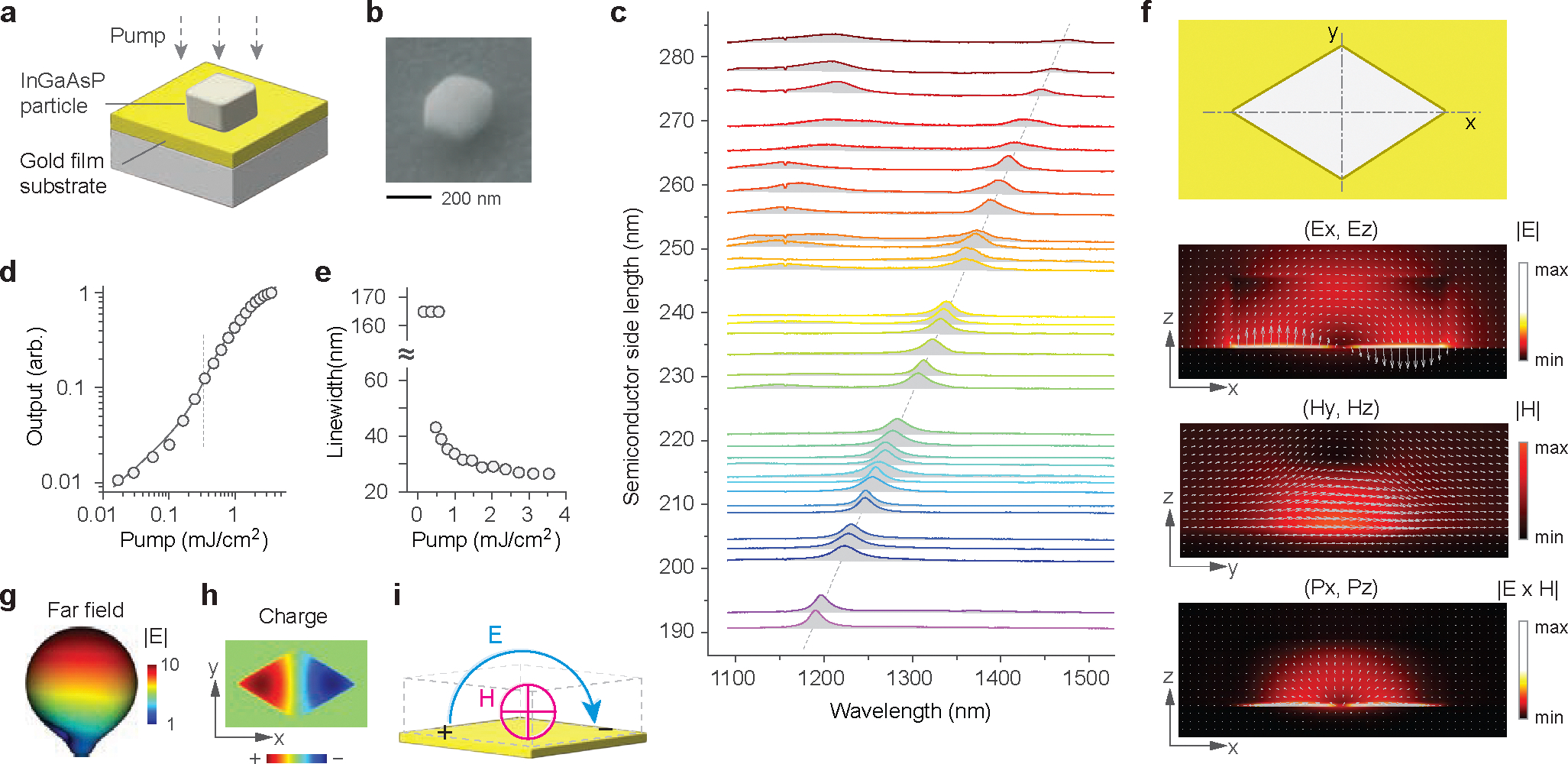
a, Schematic of the semiconductor-on-gold design. b, SEM image of an In0.53Ga0.47As0.92P0.08 particle with a side length of 170 nm (280 nm from corner to corner) and a height of 130 nm. c, Emission spectra from particles with different sizes. The dotted line indicates FDTD-calculated tuning curve. d, Measured light-light curve (circles) of a sample and theoretical fit (solid curve, ). e, Measured linewidth at different pump fluences. f, (top) Schematic top view of the half-wave device, and electromagnetic fields in a x-z cross-section in the mid plane of the device: the electric field (E), magnetic field (H), and Poynting vector (P). g, Computed far-field pattern. h, Induced charges . i, Schematic of the lowest-order magnetic dipole mode.
As the pump fluence was varied, each particle showed nonlinear intensity growth, linewidth narrowing, and a single-polarization spectral peak over quasi-unpolarized background (Extended Data Fig. 3). For instance, at room temperature one device having a size about 245 nm displayed a threshold at 350 μJ/cm2 with a fitted spontaneous emission factor () of 0.06 (Fig. 2d). Across the threshold, abrupt spectral narrowing was observed (Fig. 2e). The linewidth of the lasing mode was 45 nm at the threshold but decreased to 27 nm at higher pump powers (Extended Data Fig. 3b–d).
In the FDTD simulation, only one resonance mode was found within the broad fluorescence bandwidth. Its electromagnetic field is strongest near the metal plane, with the electric field primarily oriented perpendicular to the metal surface. Within the semiconductor, the electric field forms a loop from one side to the other, encircling the magnetic field, which oscillates along the minor axis. This configuration results in radial energy radiation (leakage) from the metal-semiconductor laser (Fig. 2f and Supplementary Fig. 3). The far-field emission can be efficiently collected in the vertical direction (Fig. 2g). With a dipolar charge distribution (Fig. 2h), this half-wave mode corresponds to a magnetic dipole (MD) mode (Fig. 2i). It is important to note that a similar MD mode is the lowest mode in cylindrical dielectric resonators37, while spheres exhibit an ED mode as the lowest. In our geometry, with the metal surface acting as a mirror, the MD mode can be interpreted as an ED mode in a flattened coordinate system (with the polar angle mapped to x-axis and the azimuthal angle to the y-axis), or as the lowest-order Mie-like transverse magnetic (TM) mode37.
Building on a standard semiconductor laser model (Fig. 3a), we formulated quasi-continuous-level rate equations in the spectral domain (Methods and Supplementary Note 3). The model did not consider expected spatial dependence in spontaneous and stimulated emission rates, nor the accompanying depletion and diffusion38 of electron-hole pairs, treating them as spatially averaged parameters. Given the band gap edge at 1570 nm and optical pumping at 1064 nm, the total number of gain emitters available is estimated to be ~1 × 1019 cm−3. This large carrier concentration is normally not achievable due to Auger recombination (~2.3 × 10⁻¹⁹ cm−6/s for InGaAsP), but is attained in plasmonic cavities due to enhanced radiative emission. Within the mode bandwidth centered at 1240 nm, the number of gain emitters is (~3.4 × 1018 cm−3 for . In a bulk semiconductor, the theoretical maximum free-space gain would be around 3,000 cm−1 at 1240 nm, which is insufficient to compensate for the cavity loss of ~17,700 cm−1 (Supplementary Note 2). The gain enhancement provided by the Purcell factor for subwavelength modes makes it possible to reach the threshold (Extended Data Fig. 4).
Fig. 3. A semiconductor laser ‘waterfall’ model.
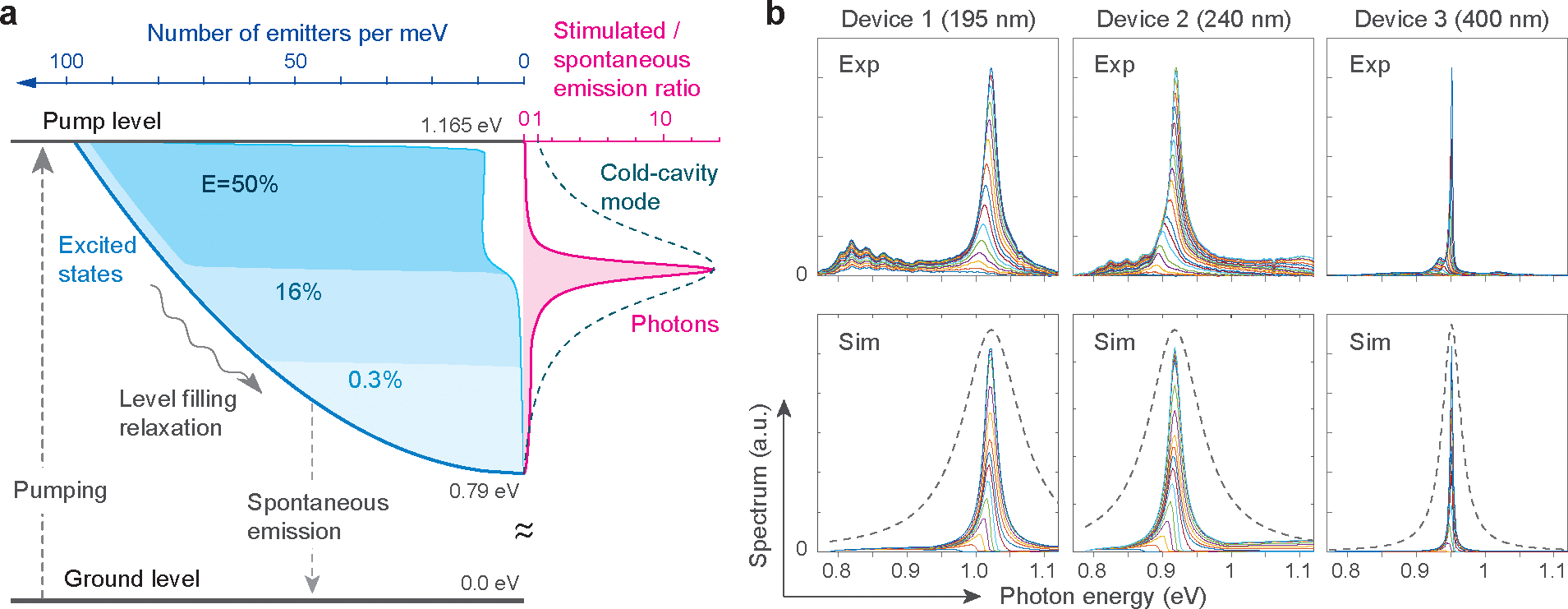
a, Energy diagram of gain emitters (electron-hole pairs) and photons (polaritons) in a cavity. The population in the excited states (bluish shades) and output spectra (cyan) are illustrated for a 240 nm-size device at a pump fluence of 0.8 mJ/cm2. In the beginning of a pump pulse (0.3% of the total pump energy), only the bottom excited states are filled. As the pump increases (to 16%), the quasi-Fermi level elevates to the mode center frequency, at which the threshold has been reached. At the peak of the pump pulse (50% energy), stimulated emission becomes greater than the spontaneous emission of the mode. See Extended Data Figure 5 and Supplementary Note 4 for more details. b, Comparison of experiments (top) and simulations (bottom) for two lowest-order devices (Device 1 with a size of 195 nm and Device 2 with a size of 240 nm, both with simulated and Purcell factor = 18) and one high-order device (Device 3 with a size of 420 nm, simulated , and Purcell factor = 8), for a range of pump fluence from 0.03 to 3 mJ/cm2. The dashed curves in the simulation represent the cavity mode spectra without gain. A periodic spectral fringe appears between 0.8 and 0.88 eV owing to internal interference in a dichroic mirror in the setup. See Extended Data Fig 6 for light-in-light-out curves and linewidths.
Remarkably, our numerical simulation closely reproduced the experimental results. Figure 3b illustrates the measured and simulated spectra of two half-wave devices and a one-wave device. At low pump powers, only spontaneous emission near the band edge is evident. As the pump increases, the excited band fills up, and the spontaneous emission peak shifts toward higher energies. With stronger pumping, photons (polaritons) accumulate in the cavity, and eventually, stimulated emission surpasses spontaneous emission within the mode’s spectral bandwidth. Upon reaching this threshold, the linewidth decreases, and the number of output photons increases nonlinearly (Extended Data Fig. 5). A kink, characteristic of a small spontaneous emission factor (), appears even when only one mode present in the gain bandwidth. This apparent kink in the light-in-light-out curve results from level filling; the amplification of the mode must wait until the quasi-Fermi level of the emitter energy reaches the mode resonance. The so-called threshold-less lasing is not possible in this case. The roll-off of the output power at higher pump levels can be attributed to increasing nonradiative Auger recombination. Ultimately, the output saturates when all excited states have been populated.
Temporal and spatial characteristics of laser output
We compared particles on a gold substrate (plasmonic devices) with those on silica-coated silicon substrates (dielectric or photonic devices). A total of 120 devices produced from 6 batches were examined, each with different average particle sizes but similar thicknesses around 290 nm (Fig. 4a and Extended Data Fig. 6). As particle size and oscillating mode order increased, the lasing threshold showed a modest decrease (Fig. 4b), while the linewidth significantly narrowed to 4–6 nm. For dielectric devices, lasing was observed only for particle sizes larger than 880 nm, even at the highest pump fluence of 8 mJ/cm2.28,29,39 Under picosecond (~70 ps) pumping with a seed-amplified laser (765 nm, 2.5 MHz), these devices required a fraction of the peak threshold power compared to nanosecond (2 ns) pumping (Extended Data Fig. 6d), primarily due to the accelerated carrier lifetime of charge carriers by the Purcell effect. Using picosecond pumping and a single-photon InGaAs avalanche photodiode, we measured the fluorescence decay time of half-wave devices to be well below the instrument’s resolution of 140 ps, a significant reduction from 1–2 ns decay time observed in pristine bulk wafers at the same pump intensities (Extended Data Fig. 7). The finite resolution prevented us from capturing theoretically expected changes in temporal profiles across the lasing threshold for the half-wave devices. For larger devices, however, resolution-limited temporal narrowing was clearly observed (Extended Data Fig. 7).
Fig. 4. Lasing threshold and far-field emission dependence on size.

a, Measured laser thresholds of several sample batches fabricated for different semiconductor sizes. The datapoint at a size of 200 nm represents a group of devices operating in the lowest-order mode, while the datapoint at 350 nm is from devices operating in the second-order modes. b, SEM images of representative samples from different batches. c, Emission spectra of a representative In0.80Ga0.20As0.44P0.56 half-wave device (mode order m = 1) in the 1000–1100 nm range at various pump fluences. Inset: SEM image of a representative particle with a size of 170 nm and a height of 200 nm. d, Light-in-light-out data corresponding to the spectra in c. e, Far-field emission patterns of the half-wave device. f, Far-field emission patterns of another half-wave device below and above the threshold. g, Schematic of the setup for imaging output emission from a device embedded beneath a scattering matrix (80-μm thick Scotch tape). h, Speckle images from three different half-wave devices below and above the threshold. i, Far-field emission patterns from a second-order device (m = 2) without (left) and with (right) a scattering matrix. j, Far-field patterns from a high-mode (m > 10) device without (left) and with (right) a scattering matrix.
To investigate far-field emission profiles, we used In0.8Ga0.2As0.44P0.56 semiconductor particles and achieved half-wave lasing in the 1000–1100 nm spectral range, which falls within the extended detection range of silicon cameras available to us. Under picosecond pumping, rhombus-shaped particles with side lengths between 150 and 200 nm and a thickness of 200 nm exhibited narrowband lasing emission with linewidths as narrow as 6 nm (Fig. 4c), with a distinct threshold at approximately 1 mJ/cm2 (Fig. 4d). FDTD simulations indicated that these samples support the half-wave mode in this spectral range, with Q factors of 10–13. The high lasing Q factor of 170 is likely due to the increased gain of this InGaAsP composition38 and the greater pump absorption (producing more carrier charges) with 765 nm light compared to 1064 nm.
The optical emission images of the half-wave devices showed circular, near diffraction-limited patterns (Fig. 4e–f). In contrast, higher-order mode devices displayed whispering gallery mode patterns above the lasing threshold (Fig. 4i–j). We further covered the devices with a translucent tape (3M Scotch Magic tape, 80 μm thick) and measured the emission through the scattering matrix (Fig. 4g), simulating intra-tissue imaging.40 As shown in Fig. 4h, the speckle patterns became more vivid above the threshold due to the narrower and spatially coherent laser emission. Higher-order mode devices exhibited more distinct changes at the threshold (Fig. 4i–j).
Plasmonic laser particles for cell barcoding
Previously, we have developed photonic laser particles (LPs) based on InGaAsP microdisks and demonstrated their applications in single-cell analyses, such as cell tracking, imaging, and flow cytometry.41–43 Miniaturized LPs are desirable for these applications, as well as super-resolution imaging44 and sensing45, as they cause minimal perturbation42, especially valuable in the NIR range outside the conventional 400–800 nm window used for fluorescence measurements.
To create metal-semiconductor LPs, we coated In0.73Ga0.27As0.58P0.42 pillars in situ on a wafer with a silica layer, followed by depositing a gold layer on top by evaporation (Fig. 5a). Electron microscopy revealed a conformal gold coating of 80–100 nm thickness found exclusively on one side (Fig. 5b and Extended Data Fig. 8), with a 5 nm-thick silica insulating layer between the semiconductor and gold (Fig. 5c and Extended Data Fig. 8). Unlike earlier substrate-based devices, the gold-InGaAsP particles with half-wavelength sizes did not reach the lasing threshold. We attributed this to the lower quality of the formed gold layers (Extended Data Fig 9a), though this can be improved.46 The smallest LP batch exhibiting lasing in air had a size of 580 nm (Fig. 5d), corresponding to a longitudinal-mode order of 3. This size is 2–3 times smaller than typical non-gold-coated InGaAsP LPs in the same spectral range. Under nanosecond pumping (1064 nm, 2 MHz), the measured emission linewidths were below 4 nm, indicating linewidth Q factors of over 250, suitable for spectral multiplexing and barcoding.
Fig. 5. Plasmonic laser particles and intracellular lasing.

a, Schematic of fabrication. b, Electron micrograph of an isolated particle. c, Elemental analysis of a gold-semiconductor particle. d, 580-nm sized samples. e, Output spectra of 31 LPs in water over a wide wavelength range with pumping at ~20 pJ/μm2 per pulse. f, FDTD simulation of a lasing mode in water. g, Microscope image of Hela cells (expressing green fluorescent protein) tagged with LPs (1 to 4, indicated by dotted circles). h, Measured spectra from the intracellular plasmonic nanolasers marked in g.
We further coated the gold-deposited InGaAsP particles with a 60 nm-thick silica layer to enhance both material and optical stability in aqueous environments. Figure 5e presents laser spectra from 31 silica-coated LPs in water, with diameters ranging from 780 to 920 nm. The single-mode tuning range extends up to 150 nm and can be further expanded by using different InGaAsP compositions. These particles operate in whispering gallery modes (Fig. 5f). Similar narrowband lasing was also observed from LPs with a thinner gold thickness of 15 nm, allowing optical pumping through the gold (Extended Data Fig. 8).
For cell tagging and biocompatibility, we functionalized silica-coated LPs with polyethyleneimine coating. After incubation with Hela cells, the polymer-coated LPs were internalized into the cytoplasm (Fig. 5g). Upon optical pumping, these intracellular lasers generated a linewidth of 4 nm (Fig. 5h). A pump energy of several picojoules per pulse and a peak power less than 1 mW are acceptable for biological applications, especially when the pump beam can be rapidly scanned across cells in imaging or flow instruments.47 No detrimental effects of LPs on cell viability were observed. Using conventional photonic LPs coated with the same polymers, we have observed minimal effects of intracellular LPs on cell division, surface receptors, and transcriptomic phenotypes.41–43 The presence of gold within polymer layers would not affect biocompatibility.
Conclusions
Our work has successfully demonstrated lasers operating at fundamental oscillation frequencies by harnessing the half-wave dipolar plasmonic mode. This achievement enables smaller device sizes compared to previous higher-order devices, even outperforming those operating at cryogenic temperatures (see Extended Data Fig. 10). The miniaturization approach may prove useful for developing high-density light source arrays for applications such as laser imaging, light detection and ranging (LiDAR)48, laser display49, photon computing50, and on-chip communications51. It is anticipated that proportionally smaller devices could be realized at shorter wavelengths down to 800 nm by using other III-V gain media, such as InP and GaAs. The substitution of gold with silver may lead to narrower linewidths. It should be possible to control the particle size and shape more precisely using advanced lithography using deep UV or nanoparticle masks.52 Our metal-semiconductor design has enabled us to produce plasmonic LPs that emit narrowband light across a broad spectral range. Compared to previously demonstrated photonic LPs in the same short-wavelength infrared (SWIR) region41,43, the plasmonic LPs are approximately 2.5 times smaller in lateral size and six times in volume and weight.
This reduction is significant and advantageous in cellular applications, particularly for small, mobile immune cells (see Supplementary Fig. 4). The smaller size minimizes physical interference with cells and their migration42, facilitates tagging cells with multiple LPs for tracking through cell division, and may enable tagging of subcellular organelles, such as nuclei. These cell-barcoding nanolasers hold promise for various applications, including large-scale multiplexed imaging, single-cell analysis, and plasmonic sensing.37,39–41
METHODS
Materials.
Custom semiconductor wafers with metal-organic chemical vapor deposition (MOCVD) epitaxial layers on InP substrates were ordered from Seen Semiconductors. Gold substrates, purchased from Platypus, had a measured surface roughness of 1.2 nm. H2SO4 was purchased from Transene Company. All other chemicals, such as H2O2, HCl, tetraethyl orthosilicate, polyethyleneimine, and ammonium hydroxide, were purchased from Sigma-Aldrich.
Half-wave device fabrication.
We used an epitaxial wafer with three layers of undoped InGaAsP with different stoichiometry, separated by InP sacrificial layers. Mesa structures were fabricated using optical lithography and reactive ion etching to a diameter of 0.9 to 1 μm. Among the three InGaAsP materials, we used In0.53Ga0.47As0.92P0.08 or In0.8Ga0.2As0.44P0.56 layers, with initial thickness of 290 or 200 nm, respectively. The diameter of the InGaAsP layer was adjusted by immersing the wafer chip in acid Piranha solution (H2SO4:H2O2:H2O = 1:1:10) and etching for a pre-calibrated reaction time.39 Next, the InP layers were removed using hydrochloric acid (HCl), which released the InGaAsP particles.41 The particles were washed with ethanol and water, then dispersed in ethanol. The InGaAsP particles were further etched in Piranha solution (H2SO4:H2O2:H2O = 1:1:10) to achieve the final desired thickness and lateral size, based on pre-calibrated reaction times. Submicron particles typically acquired rhombus shapes due to anisotropic etching rates across different lattice planes of InGaAsP. For SiO2 coating, we used Stöber method.41 Silica-coated particles were washed multiple times with ethanol and water before being drop-cast onto designated gold or silica-coated silicon substrates.
Optical measurements.
We utilized a commercial laser-scanning microscope (Olympus, FVMPE-RS) for optical characterizations. The laser-scanning unit of the microscope was coupled with both nanosecond and picosecond pump lasers. The nanosecond pump laser (IPG photonics, YLPN-1–1X120–50-M) at 1064 nm had a tunable pulse duration ranging from 1 to 120 ns and a variable repetition rate from 2 kHz to 14 MHz. For shorter pump pulses, we used a picosecond pump laser (Picoquant, VisIR-765) with a pulse duration of 70 ps, a center wavelength of 765 nm, and a repetition rate variable from 2.5 MHz to 80 MHz. A near-infrared-optimized, 100x, 0.85-NA (numerical aperture) objective (Olympus IMS LCPLN100xIR) was used for optical pumping. The output emission from samples was collected through the same lens and directed to a near-infrared spectrometer via a dichroic mirror. An InGaAs linescan camera (Sensor Unlimited 2048L) was used for spectra characterization with a typical integration time of 1 ms. The spectrometer had a diffraction grating with 200 lines per millimeter, providing a resolution of 0.8 nm and a wavelength span of 1100 to 1600 nm. For low-temperature experiments, we placed samples on a thermoelectric cooler connected to a chiller. For time-resolved photoluminescence measurements, we used a picosecond laser (VisIR-765, PicoQuant) with a repetition rate of 40 MHz, a single-photon InGaAs avalanche photodiode (Micro Photonics Devices) with a timing jitter of 100 ps, and a time-correlated single-photon counting board (TimeHarp 260, PicoQuant) with a resolution of 25 ps. For the far-field emission and speckle imaging, we employed a silicon-based EMCCD camera (Luca, Andor) in a wide-field configuration, along with a spectrometer (Shamrock, Andor) equipped with a silicon-based EMCCD (Newton, Andor) and a 300 lines/mm diffraction grating (500 nm blaze) for a resolution of 0.67 nm and. The pump source was a picosecond laser (VisIR-765, PicoQuant) at 765 nm with a 2.5 MHz repetition rate. A long-pass dichroic filter with an 850 nm cutoff were used for sample excitation and emission detection. The pump beam was expanded using a 4f telescope to approximately 15 μm full width at half maximum in the focal plane. A 3M Magic tape was applied to the sample on a gold substrate as a scattering medium. Pump excitation and detection were conducted in an epi-fluorescence configuration.
Numerical Simulations.
FDTD calculations of Mie scattering spectra and dipole-embedded cavity mode properties were performed using commercial software (Lumerical FDTD Solutions). More details are available in Supplementary Note 5.
Semiconductor laser modeling.
The rate equations of a semiconductor laser were formulated and solved numerically using MATLAB in a laptop. Briefly, the energy states of electron-hole pairs are divided into typically 120 levels (labeled 1 to k) and the numbers of emitters evolve over time via pumping (), stimulated emission (), spontaneous emission (), and non-radiative decays to lower levels . The photon numbers with energies labeled from 1 to k are varied over time through stimulated emission, spontaneous emission, and cavity loss . Thermodynamic excitation was neglected for computational simplicity.
For electron-hole pair numbers in the 1st (band edge) to the -th (pump) levels:
| (2) |
| (3) |
| (4) |
| (5) |
For photons (polaritons) in the -th levels :
| (6) |
The transition rate coefficients depend on the resonance frequency and bandwidth :
| (7) |
| (8) |
| (9) |
Details are described in Supplementary Note 3.
Fabrication of metal-coated semiconductor particles.
To produce stand-alone laser particles, we used an In0.73Ga0.27As0.58P0.42 single-layer wafer. After optical lithography and RIE etching, pillars with a diameter of ~ 2 μm were created.41 The diameter of the InGaAsP layer was reduced by immersing the wafer chip into acid Piranha solution (H2SO4:H2O2:H2O=1:1:10) for a specific etching duration.39 Subsequent HCl or H3PO4 was used to etch InP sacrificial layers to diameters roughly matching that of InGaAsP layer as well as removing an InP cap layer on top the InGaAsP layer. After washing the wafer, a 5-nm thick layer of SiO2 coating was produced on the pillars using the Stöber method. 41 A gold layer was deposited on the pillar array using an e-beam evaporator (Denton EE-4, Harvard Center for Nanoscale Systems). By immersing the wafer in HCl, the gold-deposited metal-semiconductor particles were detached from the substrate. The harvested particles were washed three times with fresh water and ethanol. To enhance material stability and biocompatibility in aqueous media and the cytoplasm, approximately 60 nm thick silica shell was added to the particles by the Stöber method in three cycles.41 To further enhance biocompatibility and facilitate cellular uptake, the silica-coated metal-semiconductor particles were encapsulated with polyethyleneimine (PEI) polymers.
Cell experiments.
Green fluorescent protein (GFP) expressing HeLa human cervical cancer cells were purchased from GenTarget. The HeLa cells were cultured in Dulbecco’s modified Eagle medium (DMEM) supplemented with 10% (v/v) fetal bovine serum (FBS) and 1% (v/v) penicillin–streptomycin, at 37 °C under 5% CO2. For cell tagging, cells at the desired density were plated on a glass-bottom plate with the cell media. Metal-semiconductor laser particles suspended in the same cell culture media were added to the cell containing plate. The plate was shaken to evenly disperse the laser particles. After 24 hours of incubation, cell laser experiments were performed using a customized microscope.
Extended Data
Extended Data Fig. 1. Mode properties of metal-semiconductor nanoparticles.

a-b, Mie scattering spectra of gold nano-spheres (a) and gold nano-disks (b) in the air for planar incident waves. While the excitation of higher order modes is evident for spheres, only the fundamental electrical dipole mode clearly appears for disks owing to the symmetry; The higher modes in disks are not efficiently excited by the uniform driving field. In nanolasers, however, the higher-order plasmonic modes are driven by local emitters and can be efficiently excited via near-field interactions. c, Schematic depicting mode coupling between plasmonic and semiconductor disk modes for three representative cases: (i) Non-lasing metallic luminescence when a semiconductor disk is too thin. Because of the large differences of the modes in energy, mode coupling is weak, and the lowest order modes are largely plasmonic. Because of the proximity of the modes, it is difficult to selectively amplify only the ED mode; (ii) Higher-order hybrid laser, where multiple dielectric-like modes are present within a gain bandwidth; (iii) A hybrid dipole laser — this may be regarded a “spaser” — where the individual modes in the metal and semiconductor disks have similar energies. Strong coupling occurs between ED modes, separating the hybrid plasmon-like mode from the other hybrid modes. This mode shift may be considered as the effect of the refractive index of the semiconductor on the plasmonic mode. However, mode coupling is a more accurate explanation as the effective index the plasmonic ED mode experiences is the same as the index of the ED mode in the dielectric medium. Note that the MD modes, the lowest order modes in dielectric disks, are not efficiently coupled with the plasmonic ED mode because of the field symmetry. d, FDTD simulation of metal-semiconductor disks with different diameters depicted in the inset. The resonance wavelength, quality factor, and mode confinement factor in the semiconductor vary as a function of the diameter ratio from 0 (III-V only) to infinity (on a gold substrate). The resonance wavelength of the hybrid ED mode increases dramatically from 600 nm to 1300 nm at size matching and then 1220 nm for oversized gold. The quality factor has the maximum at a diameter ratio of 0.5, in part due to the best mode energy matching and in part due to the lower metallic absorption at 800–900 nm. The Q factor approaches to slightly over 10 at infinite gold, where a quarter of electromagnetic energy residing in the semiconductor while the rest three quarters are stored in the metal. See Supplementary Figure S2 for more examples of Mie scattering spectra. e, Simulated Mie scattering spectra of a complex of semiconductor (n=3.5) and gold rhombus-like particles with the same side length of 250 nm and different heights of 130 nm and 100 nm, respectively, for various gap distances. The arrow indicates the lowest-order mode at the contact. f, Electric field amplitude profiles of the semiconductor-gold particles in contact (dashed outline). g, Simulated Mie scattering spectra of a semiconductor on infinite substrates for different gap distances. The arrow indicates the lowest mode at the contact. h, Electric field amplitude profiles of the semiconductor-on-gold structure. i, Simulated Mie scattering spectra of a rhombus-shaped semiconductor on an infinite substrate for different rhombus interior angles.
Extended Data Fig. 2. Size and thickness tuning of semiconductor particles.
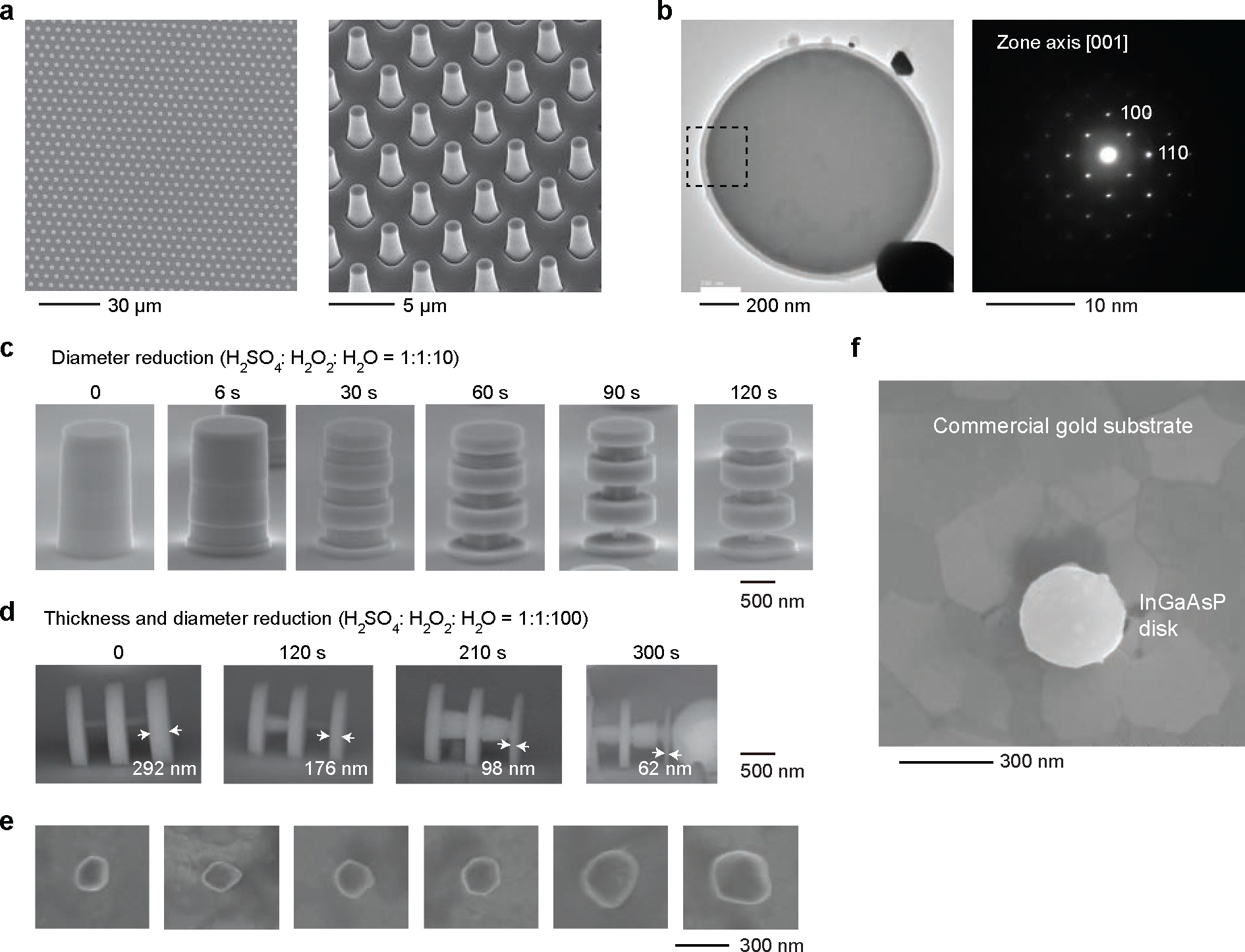
a, SEM images of a semiconductor wafer after RIE, showing pillars with a diameter of 1.21 μm ± 45 nm. b, (Left) A high-resolution transmission electron micrograph (HRTEM) of a silica-coated microdisk; (Right) an electron diffraction (SAED) pattern from a selected area (dashed square). The zone axis is labeled as 001, and two lattice plane directions, 100 and 110, are assigned for clarity. c, Two-dimensional etching for reducing the diameters of InGaAsP layers while preserving their thickness using piranha acid solution. The InP layer remains the same size while InGaAsP is etched away. The bottom layer with a composition of In0.53Ga0.47As0.92P0.08 was primarily used in most experiments (unless specified). d, Three-dimensional etching of InGaAsP layers, performed after a full (typically) or partial (for this dataset) etching of InP layers between InGaAsP layers. This process reduces both the thickness and lateral sizes. The 2D and 3D etching techniques were judiciously used to obtain desired thicknesses and sizes for InGaAsP particles. e, SEM images of six particles obtained from a single batch targeting a thickness of 130 nm and a mean side length of 250 nm. This batch was used to produce the experimental data in Figure 2c. The variation in size and shape was largely introduced during the size reduction process via wet etching. More uniform disks could be produced from reduced pillar diameters. f, SEM image of an isolated semiconductor nanodisk placed on top of a gold-coated substrate. The polycrystalline domains of the gold layer are visualized.
Extended Data Fig 3. Half-wave dipolar lasers.

a, Schematic of a microscope setup used for optical characterizations. b, Measured lasing linewidth Q factors of 40 devices with different sizes and shapes. Representative spectra are displayed in Figure 2c. c, Emission spectra of two devices at a room temperature of 298 K. d, Two devices at a Peltier cooled temperature of ~ 230 K (nominal). Compared to the room temperature spectra, the falling edges at the high energy side, or near the quasi-Fermi levels, are steeper, presumably due to slightly reduced thermal excitations at the lower temperature. Note that the computer simulation spectra exhibit ever steeper spectral falloff at the quasi-Fermi level (see Fig. 3b and Extended Data Fig. 6), because no thermal excitations have been considered in the model, which corresponds to zero-degree temperature (0 K). e, Output spectra through a polarizer at different angles. The stimulated emission peak at 0.94 eV (1321 nm) is linear polarized while the broad lower-energy background above the peak (0.75 to 0.9 eV) is approximately unpolarized.
Extended Data Fig 4. Semiconductor gain and a ‘waterfall’ laser model.

a, Energy level diagram and various transitions paths in a semiconductor laser. This forms essentially a four-level laser system (or a quasi-three-level including valence band absorption of intracavity light). The blue shade represents free electrons (or the electron-hole plasma) that fill the electronic states in the conduction band. The simplified “waterfall” model depicted in Fig, 3a is based on this diagram. b, Analysis of charge carrier loss due to Auger recombination for bulk (blue) and Purcell-enhanced (yellow) radiative decays. See Supplementary Note 2. c, Gain profiles at room temperature at three different carrier density levels, calculated using standard semiconductor theory considering the Fermi-Dirac distribution of the carriers at room temperature. The thermodynamic excitation was neglected in our numerical modeling in this work, which makes a sharp gain cliff beyond the quasi-Fermi level. d, Calculated total carrier density versus transparency (zero-gain) wavelength. e, Simulated output spectra of a device with a size of 240 nm for the cases of different Purcell factors, from 1 to 30, as the pump fluence is varied from 0.021 to 2.1 mJ/cm2. The output saturates. Dashed curve illustrates the cold-cavity mode profile with a Q factor of 10. At , lasing threshold is never reached even at extreme pumping. At , lasing threshold is barely reached with a stimulated-to-spontaneous ratio of 1.07. Compared to results in reduced linewidths. Best correspondence to experimental data was obtained with (Device 1) and (Device 2). f, (Left) The emitter population and stimulated-to-spontaneous ratio at a threshold pump fluence, at which the quasi-Fermi level is just below the modal resonant frequency. (Right) At a pump level 7.3 times above the threshold when all the entire excited states are almost filled.
Extended Data Fig 5. Laser simulation and experimental results.

a, Half-wave device (semiconductor volume: 183 × 183 × 130 nm3). b, Half-wave device (225 × 225 × 130 nm3). c, One-wave device (400 × 400 × 130 nm3).
Extended Data Fig 6. Higher-order mode devices.

a-b, Representative devices from different batches of varying sizes (same thickness of 290 nm) for plasmonic (a) and dielectric cavities (b). Dielectric devices with less than 880 nm sizes did not reach lasing threshold even at the highest pump power levels. c, Emission linewidths measured from a total 120 devices. The threshold pump fluences of these devices are shown in Figure 2. d, The ratio between the peak threshold powers for picosecond and nanosecond pumping. e, FDTD results of a 350-nm rhombus-shape showing a second order mode at 1206 nm (top) and a rectangular-shape 500-nm device showing a whispering gallery mode (Q = 94) at 1164 nm (bottom).
Extended Data Fig. 7. Temporal responses of picosecond-pumped devices.

a-e, Output intensity (left) and temporal (right) curves at varying pump powers from four representative devices: a, pristine semiconductor wafer; b, a photonic microlaser with a diameter of approximately 2 μm placed on a glass substrate; c, a plasmonic nanodisk device with a diameter of approximately 350 nm on a gold substrate; and d-e, two different nanodisk devices with a diameter of approximately 230 nm on a gold substrate. Colors represent measurements at different pump powers. All laser devices exhibit kink behaviors indicative of the lasing threshold and accelerated lifetime. f, Superimposition of three representative spectra obtained from the devices in a, b, and d, above their respective lasing thresholds. The temporal profiles in the vicinity of the peak are nearly identical, indicating they are limited by the finite temporal resolution of the measurement instrument.
Extended Data Fig 8. Structure of metal-semiconductor particles.

a, Schematic and SEM images of disk-on-pillar array following SiO2 coating and gold deposition. b, Bright-field and SEM images of plasmonic laser particles drop casted on a silica-coated silicon substrate, presenting both the III/V side (left) and the Au side (right). c, Transmission Electron Microscopy (TEM) image of a cross-section of a sample, prepared by using focused ion-beam (FIB) etching. The image reveals the InGaAsP layer with a thickness of ~290 nm, 5–7 nm thick SiO2 layer, and ~ 80-nm thick gold layer. d, Higher magnification view of the cross section. e-f, Scanning transmission electron microscopy (STEM) images and elemental maps. The samples in c-f were prepared by placing the InGaAsP side on a silica-coated silicon substrate and deposited Ga on top of the Au side of the particles. The samples were then placed up-side down on a TEM grid.
Extended Data Fig 9. Emission spectra of isolated plasmonic LPs.

a, SEM image of a semiconductor particle after electron-beam gold deposition. The deposited gold layer appears noticeably rougher that the ‘ultra-flat’ gold substrate shown in Extended Data Fig 2f. b, SEM images of samples with a gold thickness of 100 nm and a side length of 580 nm. c, Emission spectra at varying pump fluences. d, Light-in-light-out curves measured (circles) along with a theoretical fit (red curve). e, Output spectral of 4 LPs. f, Evolution of output spectra of two LPs at pump fluences varying from 0.1 to 4 mJ/cm2. The Q factor of the fourth order longitudinal mode in these devices is estimated to be 42. g, SEM images of two samples after gold deposition with a thickness of 15 nm. h, The output spectra of two thin-gold-coated samples. The Q factor of the fourth order mode in these devices is estimated to be approximately 30.
Extended Data Fig 10.

Device volume (top) and the mode order (bottom) of single particle and micro- and nanolasers operating at room temperature (cyan circles) and cryogenic temperature (pink circles). Each data point is labeled with the device name used in Supplementary Tables 1 and 2. Numerous non-metallic lasers based on periodic distributed feedback, photonic crystal reflection, and lattice structures, which operate in their lowest photonic modes, are not included in this tables since their device sizes exceed multiple wavelengths. Metal-coated lasers in C1 and C5 demonstrate photonic-like modes but not the overall lowest-order plasmonic modes.
Supplementary Material
Acknowledgements
Drs. Kwonhyeon Kim, Yue Wu, and Debarghya Sarkar are acknowledged for helpful discussions. This study was supported by National Institutes of Health research grants (R01-EB033155, R01-EB034687). S.C. acknowledges the MGH Fund for Medical Discovery fundamental research fellowship award. This research used the resources of the Center for Nanoscale Systems, part of Harvard University, a member of the National Nanotechnology Coordinated Infrastructure, supported by the National Science Foundation under award number 1541959.
Footnotes
Competing interests
The authors declare the following competing interests: N.M. and S.H.Y. have financial interests in LASE Innovation Inc., a company focused on commercializing technologies based on laser particles. The financial interests of N.M. and S.H.Y. were reviewed and are managed by Mass General Brigham in accordance with their conflict-of-interest policies. The other authors declare no competing interests.
Code availability
The semiconductor laser modeling and laser experiment data analysis code used within this paper are available through both Code Ocean and Harvard Dataverse at https://doi.org/10.7910/DVN/AOWZN8. The details of FDTD simulations and semiconductor laser modeling can be found in Methods and Supplementary Information. The associated codes can be obtained from the authors upon a reasonable request.
Data availability
The laser experiment data used within this paper are available through Harvard Dataverse at https://doi.org/10.7910/DVN/AOWZN8. The authors can provide additional data that supports the findings of this study upon a reasonable request.
References
- 1.Kogelnik H & Shank CV Coupled-wave theory of distributed feedback lasers. J Appl Phys 43, 2327–2335 (1972). [Google Scholar]
- 2.Akahane Y, Asano T, Song B-S & Noda S High-Q photonic nanocavity in a two-dimensional photonic crystal. Nature 425, 944–947 (2003). [DOI] [PubMed] [Google Scholar]
- 3.Nozaki K, Kita S & Baba T Room temperature continuous wave operation and controlled spontaneous emission in ultrasmall photonic crystal nanolaser. Opt Express 15, 7506–7514 (2007). [DOI] [PubMed] [Google Scholar]
- 4.Mao X-R, Shao Z-K, Luan H-Y, Wang S-L & Ma R-M Magic-angle lasers in nanostructured moiré superlattice. Nat Nanotechnol 16, 1099–1105 (2021). [DOI] [PubMed] [Google Scholar]
- 5.Luan H-Y, Ouyang Y-H, Zhao Z-W, Mao W-Z & Ma R-M Reconfigurable moiré nanolaser arrays with phase synchronization. Nature 624, 282–288 (2023). [DOI] [PubMed] [Google Scholar]
- 6.Hill MT et al. Lasing in metallic-coated nanocavities. Nat Photonics 1, 589–594 (2007). [Google Scholar]
- 7.Yu Y, Lakhani A & Wu MC Subwavelength metal-optic semiconductor nanopatch lasers. Opt. Express 18, (2010). [DOI] [PubMed] [Google Scholar]
- 8.Berini P & De Leon I Surface plasmon-polariton amplifiers and lasers. Nat Photonics 6, 16–24 (2012). [Google Scholar]
- 9.Oulton RF et al. Plasmon lasers at deep subwavelength scale. Nature 461, 629–632 (2009). [DOI] [PubMed] [Google Scholar]
- 10.Maslov AV & Ning C-Z Size reduction of a semiconductor nanowire laser by using metal coating. in Physics and simulation of optoelectronic devices XV vol. 6468 138–144 (SPIE, 2007). [Google Scholar]
- 11.Azzam SI et al. Ten years of spasers and plasmonic nanolasers. Light Sci Appl 9, 1–21 (2020). [DOI] [PMC free article] [PubMed] [Google Scholar]
- 12.Ma R-M & Oulton RF Applications of nanolasers. Nat. Nanotechnol 14, 12–22 (2019). [DOI] [PubMed] [Google Scholar]
- 13.Khajavikhan M et al. Thresholdless nanoscale coaxial lasers. Nature 482, 204 (2012). [DOI] [PubMed] [Google Scholar]
- 14.Lu Y-J et al. Plasmonic nanolaser using epitaxially grown silver film. Science 337, 450–453 (2012). [DOI] [PubMed] [Google Scholar]
- 15.Wu C-Y et al. Plasmonic green nanolaser based on a metal–oxide–semiconductor structure. Nano Lett 11, 4256–4260 (2011). [DOI] [PubMed] [Google Scholar]
- 16.Ma R-M, Oulton RF, Sorger VJ, Bartal G & Zhang X Room-temperature sub-diffraction-limited plasmon laser by total internal reflection. Nat Mater 10, 110–113 (2011). [DOI] [PubMed] [Google Scholar]
- 17.Sidiropoulos TPH et al. Ultrafast plasmonic nanowire lasers near the surface plasmon frequency. Nat Phys 10, 870–876 (2014). [Google Scholar]
- 18.Kwon S-H et al. Subwavelength plasmonic lasing from a semiconductor nanodisk with silver nanopan cavity. Nano Lett 10, 3679–3683 (2010). [DOI] [PubMed] [Google Scholar]
- 19.Nezhad MP et al. Room-temperature subwavelength metallo-dielectric lasers. Nat Photonics 4, 395–399 (2010). [Google Scholar]
- 20.Oulton RF, Sorger VJ, Genov DA, Pile DFP & Zhang X A hybrid plasmonic waveguide for subwavelength confinement and long-range propagation. Nat Photonics 2, 496–500 (2008). [Google Scholar]
- 21.Huang J, Kim S-H & Scherer A Design of a surface-emitting, subwavelength metal-clad disk laser in the visible spectrum. Opt Express 18, 19581–19591 (2010). [DOI] [PubMed] [Google Scholar]
- 22.Zhou W et al. Lasing action in strongly coupled plasmonic nanocavity arrays. Nat Nanotechnol 8, 506 (2013). [DOI] [PubMed] [Google Scholar]
- 23.Bergman DJ & Stockman MI Surface plasmon amplification by stimulated emission of radiation: quantum generation of coherent surface plasmons in nanosystems. Phys Rev Lett 90, 27402 (2003). [DOI] [PubMed] [Google Scholar]
- 24.Kewes G et al. Limitations of particle-based spasers. Phys Rev Lett 118, 237402 (2017). [DOI] [PubMed] [Google Scholar]
- 25.Wang Z, Meng X, Kildishev AV, Boltasseva A & Shalaev VM Nanolasers enabled by metallic nanoparticles: from spasers to random lasers. Laser Photon Rev 11, 1700212 (2017). [Google Scholar]
- 26.Wu H et al. Plasmonic nanolasers: Pursuing extreme lasing conditions on nanoscale. Adv Opt Mater 7, 1900334 (2019). [Google Scholar]
- 27.Lu Y-J et al. All-color plasmonic nanolasers with ultralow thresholds: autotuning mechanism for single-mode lasing. Nano Lett 14, 4381–4388 (2014). [DOI] [PubMed] [Google Scholar]
- 28.Wang S et al. Unusual scaling laws for plasmonic nanolasers beyond the diffraction limit. Nat Commun 8, 1889 (2017). [DOI] [PMC free article] [PubMed] [Google Scholar]
- 29.Cho S, Yang Y, Soljačić M & Yun SH Submicrometer perovskite plasmonic lasers at room temperature. Sci Adv 7, eabf3362 (2021). [DOI] [PMC free article] [PubMed] [Google Scholar]
- 30.Noginov MA et al. Demonstration of a spaser-based nanolaser. Nature 460, 1110–1112 (2009). [DOI] [PubMed] [Google Scholar]
- 31.Park Y-S, Roh J, Diroll BT, Schaller RD & Klimov VI Colloidal quantum dot lasers. Nat Rev Mater 6, 382–401 (2021). [Google Scholar]
- 32.Galanzha EI et al. Spaser as a biological probe. Nat Commun 8, 15528 (2017). [DOI] [PMC free article] [PubMed] [Google Scholar]
- 33.Peña O & Pal U Scattering of electromagnetic radiation by a multilayered sphere. Comput Phys Commun 180, 2348–2354 (2009). [Google Scholar]
- 34.Feigenbaum E & Orenstein M Ultrasmall volume plasmons, yet with complete retardation effects. Phys Rev Lett 101, 163902 (2008). [DOI] [PubMed] [Google Scholar]
- 35.Meier M & Wokaun A Enhanced fields on large metal particles: dynamic depolarization. Opt Lett 8, 581–583 (1983). [DOI] [PubMed] [Google Scholar]
- 36.Wang F & Shen YR General properties of local plasmons in metal nanostructures. Phys Rev Lett 97, 206806 (2006). [DOI] [PubMed] [Google Scholar]
- 37.Rybin MV et al. High-Q supercavity modes in subwavelength dielectric resonators. Phys. Rev. Lett. 119, 243901 (2017). [DOI] [PubMed] [Google Scholar]
- 38.Olsen G & Zamerowski T Vapor-phase growth of (In, Ga)(As, P) quaternary alloys. IEEE J Quantum Electron 17, 128–138 (1981). [Google Scholar]
- 39.Sarkar D et al. Ultrasmall InGa(As)P dielectric and plasmonic nanolasers. ACS Nano 17, 16048–16055 (2023). [DOI] [PMC free article] [PubMed] [Google Scholar]
- 40.Bernstein L et al. Ultrahigh resolution spectral-domain optical coherence tomography using the 1000–1600 nm spectral band. Biomed Opt Express 13, 1939–1947 (2022). [DOI] [PMC free article] [PubMed] [Google Scholar]
- 41.Martino N et al. Wavelength-encoded laser particles for massively-multiplexed cell tagging. Nat Photonics 13, 720–727 (2019). [DOI] [PMC free article] [PubMed] [Google Scholar]
- 42.Fikouras AH et al. Non-obstructive intracellular nanolasers. Nat Commun 9, 4817 (2018). [DOI] [PMC free article] [PubMed] [Google Scholar]
- 43.Kwok SJJ et al. High-dimensional multi-pass flow cytometry via spectrally encoded cellular barcoding. Nat Biomed Eng 8, 310–324 (2024). [DOI] [PMC free article] [PubMed] [Google Scholar]
- 44.Cho S, Humar M, Martino N & Yun SH Laser particle stimulated emission microscopy. Phys Rev Lett 117, 193902 (2016). [DOI] [PMC free article] [PubMed] [Google Scholar]
- 45.Schubert M et al. Monitoring contractility in cardiac tissue with cellular resolution using biointegrated microlasers. Nat Photonics 14, 452–458 (2020). [Google Scholar]
- 46.Maniyara RA et al. Tunable plasmons in ultrathin metal films. Nat Photonics 13, 328–333 (2019). [Google Scholar]
- 47.Yun SH & Kwok SJJ Light in diagnosis, therapy and surgery. Nat Biomed Eng 1, 8 (2017). [DOI] [PMC free article] [PubMed] [Google Scholar]
- 48.Li B, Lin Q & Li M Frequency–angular resolving LiDAR using chip-scale acousto-optic beam steering. Nature 620, 316–322 (2023). [DOI] [PubMed] [Google Scholar]
- 49.Zhao J et al. Full-color laser displays based on organic printed microlaser arrays. Nat Commun 10, 870 (2019). [DOI] [PMC free article] [PubMed] [Google Scholar]
- 50.Chen Z et al. Deep learning with coherent VCSEL neural networks. Nat Photonics 17, 723–730 (2023). [Google Scholar]
- 51.Wang Y, Holguín-Lerma JA, Vezzoli M, Guo Y & Tang HX Photonic-circuit-integrated titanium: sapphire laser. Nat Photonics 17, 338–345 (2023). [Google Scholar]
- 52.Totzeck M, Ulrich W, Göhnermeier A & Kaiser W Pushing deep ultraviolet lithography to its limits. Nat Photonics 1, 629–631 (2007). [Google Scholar]
Associated Data
This section collects any data citations, data availability statements, or supplementary materials included in this article.
Supplementary Materials
Data Availability Statement
The laser experiment data used within this paper are available through Harvard Dataverse at https://doi.org/10.7910/DVN/AOWZN8. The authors can provide additional data that supports the findings of this study upon a reasonable request.