

Abstract
Carbon‐based CsPbI2Br perovskite solar cells (PSCs) free of a hole‐transport layer (HTL) have emerged as promising photovoltaics due to their low processing cost and superior stability. However, the voltage deficit resulting from inefficient carrier extraction causes insufficient power conversion efficiency (PCE), severely hindering their progress. Here, a gradient electron energy level modulation strategy proves effective in reducing voltage losses through the rapid extraction of photogenerated electrons. This process enhances carrier separation/collection and reduces recombination at the back contact, thereby achieving high‐performance photovoltaics. It is demonstrated that the front electron extraction, equally critical as the prevailing back perovskite/carbon contact, accounts for the significant contributing factor of voltage deficit in carbon‐based HTL‐free PSCs. The resulting PSCs deliver a record open‐circuit voltage (V OC) of 1.41 V and a PCE of 17.42% and retain more than 92% of their initial efficiency after 1, 000 h. These results highlight the significant potential of carbon‐based HTL‐free perovskite photovoltaics.
Keywords: carbon‐based perovskite solar cells, electron extraction, gradient electron energy level, hole‐transport layer free, voltage deficit
A gradient electron energy level strategy is constructed to reduce voltage losses in planar HTL‐free CsPbI2Br C‐PSCs. This electron extraction optimization enables rapid photogenerated electron extraction and carrier separation, thereby suppressing recombination at the back contact. The resulting PSCs deliver a record V OC of 1.41 V, a high PCE of 17.42% and a high stability, simultaneously.

1. Introduction
Metal halide perovskites have recently attracted extensive interest as solution‐processed photovoltaics, owing to their excellent optoelectronic properties.[ 1 , 2 , 3 , 4 ] Perovskite solar cells (PSCs) have achieved remarkable breakthroughs in power conversion efficiency (PCE), with certified values exceeding 26%.[ 5 , 6 , 7 ] However, persistent challenges arising from the widely used noble metal electrodes—including metal electrode corrosion, vacuum deposition complexity, and high cost—hinder their large‐scale deployment.[ 8 , 9 , 10 , 11 ] By contrast, carbon‐based PSCs (C‐PSCs) are an alternative platform with improved long‐term operational stability owing to the chemical robustness and hydrophobicity of carbon electrode.[ 12 , 13 , 14 ] Additionally, the porous carbon black serves as an effective hole collector, enabling ambient non‐vacuum fabrication of hole‐transport layer (HTL) ‐free PSCs and streamlining manufacturing processes for cost‐effective large‐scale production.[ 15 , 16 ]
Compared with organic–inorganic hybrid halide perovskite, all‐inorganic iodide‐bromide perovskites are considered promising candidates for highly stable HTL‐free C‐PSCs owing to their stabilized crystal structure, yet their PCE remains lower than that of carbon‐based organic–inorganic counterparts.[ 17 , 18 , 19 ] This performance gap stems from two primary factors: i) Unsatisfactory crystallization control causes internal defect and unexpected spontaneous phase transition, thereby aggravating non‐radiative recombination;[ 20 , 21 ] ii) Energy level misalignment between the perovskite and extraction layer impairs carrier extraction and increases carrier recombination.[ 22 , 23 ] Experiences from metal‐electrode‐based all‐inorganic PSCs have significantly advanced crystallization modulation strategies, enhancing crystal quality and morphological control in C‐PSCs.[ 24 , 25 ] However, existing research predominantly focuses on energy level optimization at the back perovskite/carbon interface to resolve inefficient charge extraction/collection and consequent open‐circuit voltage (V OC) losses.[ 26 , 27 ] Systematic investigations of electron extraction optimization remain lacking, which is essential for developing high‐cost‐efficiency C‐PSCs. Additionally, while encouraging progress has been achieved, V OC remains a significant bottleneck, for example, for CsPbI2Br (bandgap of ≈1.9 eV) based HTL‐free C‐PSCs, V OC is limited as low as 1.33 V, with significant V OC deficit.[ 28 ]
In this work, we tackled this challenge in a counter‐intuitive way by systematically modulating electron dynamics. We demonstrate the long‐distance diffusion of electrons toward the back carbon electrode is constrained by employing a magnesium‐tin dioxide (Mg‐SnO2) quantum dots (QDs) to construct a gradient electron transport bilayer (ETL). This electron extraction optimization enables rapid photogenerated electron extraction and carrier separation, thereby suppressing recombination at the back contact. The resulting devices achieve a record V OC of 1.41 V (bandgap of ≈1.9 eV) and a high efficiency of 17.3% for planar HTL‐free CsPbI2Br C‐PSCs—the highest reported V OC for this architecture to date. Remarkably, the excellent efficiency is coupled with outstanding stability, establishing these devices as one of the most stable and high‐performance carbon‐based CsPbI₂Br HTL‐free PSCs.
2. Results and Discussion
The HTL‐free C‐PSCs were prepared with a layered architecture of FTO/ ETL/perovskite/carbon electrode. The CsPbI2Br perovskite films were deposited using a one‐step spin‐coating method from its precursor on ETL. To evaluate the impact of electron extraction on device performance, we designed three ETLs with the structure of pristine titanium dioxide (TiO2), TiO2/ commercial tin dioxide (SnO2) bilayer, and TiO2/Mg‐SnO2 QDs bilayer. This design stems from prior findings that Mg incorporation raises the Fermi level, suppresses defect states and enhances SnO2 conductivity.[ 29 , 30 ] The films and devices are named using the structure of corresponding ETL, i.e., L─T, L─TS, and L─TMS, respectively.
The current density–voltage (J–V) measurements were recorded using a solar simulator under AM 1.5G illumination. Figure 1a displays the representative J–V curves of L─T, L─TS, and L─TMS C‐PSCs. The L─T device shows a relatively low PCE of 11.18%, with V OC, current density (J SC), and fill factor (FF) of 1.21 V, 14.31 mA cm−2, and 64.62%, respectively. After modifying TiO2 with SnO2 (L─TS), the J SC, V OC, and FF of C‐PSCs are slightly enhanced, achieving an improved PCE of 14.38%. By contrast, the optimized L─TMS PSCs achieves an optimized PCE of 17.42%, along with a boosted V OC of 1.38 V, a J SC of 15.94 mA cm−2, and a FF of 79.45%, as summarized in the insert of Figure 1a. The external quantum efficiency (EQE) curve of the champion device is illustrated in Figure 1b. The integrated current density accords with the J–V measurements.[ 19 , 31 , 32 , 33 ] The statistical V OC data of L─TMS C‐PSCs in Figure 1c highlight a remarkable voltage enhancement, peaking at 1.41 V in a representative device with a PCE of 17.22% (a J SC of 15.73 mA cm−2, and a FF of 77.64%, Figure S1, Supporting Information).
Figure 1.
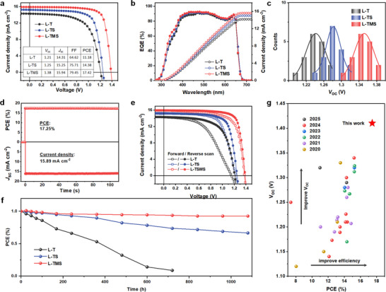
Performance of PSCs. a) J–V curves. b) EQE spectra. c) Statistical V OC distribution of PSCs. d) Steady‐state current density at maximum point and corresponding PCE. e) J–V curves of PSCs under reverse and forward scans. f) Stability test of PSCs under simulated solar light illumination (AM 1.5, 100 mW cm−2, open‐circuit condition). g) A comparison of device PCE & V OC with the state‐of‐the‐art HTL‐free CsPbI2Br C‐PSCs reported in literature (Table S1, Supporting Information).
To verify the reliability of the J–V measurements, the steady‐state photocurrent L─TMS device measured at the maximum power point (1.18 V) is recorded in Figure 1d, delivering a steady‐state efficiency of 17.25%, which confirms the performance parameters extracted from the J–V curve. Figure 1e presents minimal photocurrent hysteresis in the L─TMS device under the reverse and forward scans compared to L─T and L─TS based C‐PSCs, further supporting the reliability of the performance measurements. Figure 1f depicts the photostability of PSCs under constant AM 1.5G illumination (open‐circuit condition). The L─TMS device retains over 92% of its initial PCE after 1000 h, while the performance of L─T and L─TS devices rapidly degrades. Open‐circuit condition intentionally avoids charge extraction, allowing photogenerated carriers to recombine within the device. This accelerates voltage‐related degradation mechanisms such as ion migration, phase instability, and interfacial chemical reactions, which are directly tied to the built‐in electric field and prolonged high‐voltage exposure.[ 2 ] The enhanced device stability is attributed to improved physical contact, reduced interfacial physical defects, and decreased carrier recombination, which will be discussed later. Table S1 (Supporting Information) compares the photovoltaic parameters of the L─TMS devices with other state‐of‐the‐art HTL‐free C‐PSCs, and Figure 1g presents the corresponding PCE‐V OC distribution. These results demonstrate that our device achieves the highest V OC and PCE among all HTL‐free CsPbI2Br based C‐PSCs to date.
To clarify the difference in PSCs performance, particularly the improved V OC, we conducted the UV photoelectron spectroscopy (UPS) measurements (Figures S2 and S3, Supporting Information) to investigate carrier transport mechanisms. Figure 2a and Table S2 (Supporting Information) depict the corresponding energy‐level diagrams of PSCs. The work function of pristine L─T film is 4.71 eV, while that of L─TS decreases to 4.33 eV. By contrast, the work function of L─TMS further decreases to 3.90 eV. According to the energy levels of perovskite, L─T, L─TS, and L─TMS, the energy level alignments under the thermal equilibrium state are shown in Figure 2a. The contact between perovskite and both L─T and L─TS exhibits Schottky barriers, causing energy level mismatch and blocking electrons transfer from perovskite to ETLs. Employment of L─TMS eliminates these potential barriers, thus improving electron collection and enhancing J SC and V OC.
Figure 2.
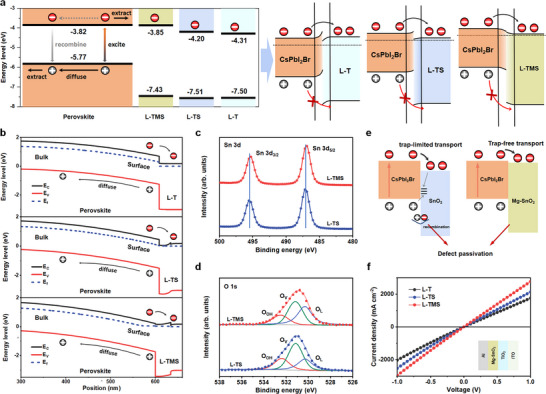
Energy level and carrier transportation in PSCs. a) Energy level diagram of PSCs at electron selective contact and their corresponding thermal equilibrium band structures. b) Calculated energy levels of PSCs with different ETL. High‐resolution XPS results of Sn 3d c) and O 1s d) signals for L─TS and L─TMS films. e) Schematic illustration of carrier transport from perovskite to SnO2 or Mg‐SnO2. f) The J–V curves of the ITO/ETL/Al films.
The energy level shift of PSCs with different ETLs were calculated to understand the role of gradient energy level alignment under thermodynamic equilibrium. As shown in Figure 2b, perovskite exhibits a downward energy‐level bending, forming a large cliff‐type energy difference with TiO2. In PSCs with this cliff structure, electrons and holes accumulate near the interface after charge separating, causing interfacial recombination via back‐transfer pathway (e.g., recombination between injected electrons in TiO2 and free holes in perovskite through deep‐level defects at interface) and resulting in serious V OC deficit, as reported in other systems.[ 33 , 34 ] Inserting SnO2 between TiO2 and perovskite reduces this cliff‐type energy difference, accounting for the improved V OC in L─TS devices. Notably, replacing SnO2 with Mg‐SnO2 further minimizes the energy‐level mismatch and introduces a conduction‐band “spike” at the Mg‐SnO2 and TiO2 interface. The spike limits the electron back‐transport to Mg‐SnO2 and thus decreases interfacial recombination.[ 35 ] Additionally, the structural uniformity of SnO2 QDs creates coherent electronic pathways, significantly enhancing electron collection efficiency.[ 29 , 30 ] In short, the shallow Fermi level at the perovskite surface drives spontaneous electron flow from the bulk to the surface, creating a back‐surface field aligned with the built‐in electric field. Meanwhile, the heterogeneous contact of perovskite/Mg‐SnO2/TiO2 creates a better and uniform gradient heterojunction, reducing the energy‐level potential barrier between perovskite and the ITO electrode. This synergy facilitates rapid electron extraction while inhibiting back‐transport, ultimately increasing J SC and V OC.[ 36 ] Figure S4a (Supporting Information) shows the calculated J–V curves of PSCs using different ETLs, which suggests the significant influence of electron extraction on increasing J SC and V OC, consistent with our above theory. We further verified our results by changing the thickness of Mg‐SnO2 layer. As shown in Figure S4b (Supporting Information), increasing thickness of Mg‐SnO2 QDs decreases J SC, V OC, and FF of C‐PSCs, simultaneously, which is attributed to the obstructed electronic transmission inside of Mg‐SnO2 layer. Conversely, although the thinner Mg‐SnO2 increases current density, we observed a reduced FF of C‐PSCs, which might be caused by the increased carrier recombination at the perovskite/Mg‐SnO2 interface due to electron back‐transfer through the thin Mg‐SnO2 layer.
X‐ray photoelectron spectroscopy (XPS) measurements were further conducted to analyze the effect of Mg‐SnO2 layer on interfacial defect recombination. Figure S5 (Supporting Information) shows the Mg 2p core‐level spectra, where the enhanced peak intensity at ≈50.2 eV confirms successful Mg incorporation into SnO2. No shift was observed for Ti 2p peaks, indicating no chemical interaction between SnO2/Mg‐SnO2 QDs and TiO₂. In Figure 2c, the Sn 3d5/2 and 3d3/2 peaks shift to lower binding energy for Mg‐SnO2 films, attributed to the formation of Sn─O─Mg bonds. The binding energy peak position of core electrons depends on the element's oxidation state and local chemical environment. When the electron density increases, the peak position shifts to a low binding energy due to the strengthened screening effect of the valence electrons.[ 29 ] The electronegativity of the Mg atoms (1.31) in Mg‐SnO2 is lower than that of the base Sn atoms (1.96). More electrons are attracted to the Sn atoms, and hence the binding energy peak of the Sn─O bonds shifts to a low binding energy. Additionally, the Sn 3d5/2 and 3d3/2 spin doublet shows an identical energy separation of 8.4 eV, confirming Sn4+ state across all films.[ 30 ]
Figure 2d shows the O 1s core level spectra of the XPS measurements, which presents slight asymmetry with a distinct shoulder for all samples. The O 1s peaks slightly shift downward for the L─TMS samples, consistent with the formation of the Sn─O─Mg bond. The O 1s core level peak can be further deconvoluted into three peaks, as shown in Figure 2d. One component centered at ≈532.4 eV indicates the presence of a hydroxyl (─OH) group on the SnO2 surface. The two other components, found at lower binding energy ≈531.6 and ≈530.3 eV, are assigned to the oxygen vacancies (V O) and lattice oxygen (oxygen directly bounded to a metal atom), respectively.[ 37 ] The introduction of Mg reduces oxygen vacancy density in the semiconductor due to the changed electron cloud density around Sn atoms. This reduces the defect states, restrains their detrimental effect on back‐transfer charge recombination, and improves the electron extraction of ETL.[ 38 ] Consequently, the L─TMS layer promotes interfacial charge extraction and transport, contributing to a high V OC (Figure 2e).
We systematically compared the electrical conductivities of L─T, L─TS, and L─TMS ETLs using lateral conductivity measurements (ITO/ETLs/Al architecture, Figure 2f). The hierarchical SnO₂/TiO₂ heterostructure in L─TS and L─TMS facilitates gradient‐driven electron injection, as evidenced by the monotonically increasing current density across the series (L─T < L─TS < L─TMS). This enhancement directly correlates with the optimized energy‐level alignment at the ETL/perovskite interface, which minimizes carrier injection barriers and improves electron collection. Complementary time‐resolved photoluminescence (TRPL) spectroscopy of perovskite films on different ETLs (375 nm excitation from the ITO side) further elucidates interfacial charge extraction dynamics. As shown in Figure S6 (Supporting Information), the PL decay lifetimes (τavg) trend to decrease in the films of L─T (32.64 ns), L─TS (24,50 ns), and L─TMS (22.12 ns) (Table S3, Supporting Information). The reduced PL lifetime in L─TMS confirms its superior electron extraction capability, which synergistically contributes to the observed enhancements in J SC and V OC.
To further understand the dynamic process of photoelectric conversion in PSCs, we investigated the influence of ETL on carrier generate, transfer and recombination by device simulation using COMSOL Multiphysics (V6.0) software based on a simplified 2D numerical simulation. The perovskite films with the same thickness are sandwiched between the carbon electrodes and different ETLs attached with the ITO electrode. The simulation reveals that in all configurations, the photo‐generated carriers are concentrated near the ETL interface (Figure 3a), gradually diminishing from the interface to the perovskite and accompanying by several small peaks.[ 39 ] Incident light traverses the transparent ITO electrode and is absorbed predominantly near the ETL/perovskite interface (Figure 3a). This creates a high‐density population of photogenerated electrons and holes proximal to ETL. Electrons are rapidly collected by the gradient Mg‐SnO2/TiO2 ETL (L─TMS) due to its optimized energy‐level alignment (Figure 2a), minimizing the existing time in the perovskite bulk. Simultaneously, holes diffuse across the perovskite layer toward the carbon electrode, driven by a pronounced hole concentration gradient established by efficient electron extraction (Figure 3b). The spatial separation of electrons (extracted via ETL) and holes (diffused to carbon) minimizes electron‐hole encounters, suppressing recombination near the back contact. In contrast, poor electron extraction in conventional L─T or L─TS structures allows electrons to diffuse toward the carbon electrode, increasing spatial overlap with holes near the back contact of carbon. This overlap leads to significant bimolecular recombination.[ 40 ]
Figure 3.
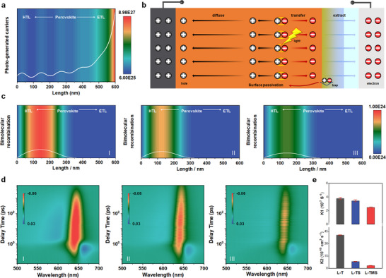
Carrier dynamics. a) The distributions of photo‐generated carrier. b) device configuration model for simulation and the proposed carrier behavior. c) The distributions of electron‐hole recombination rate in PSCs with different ETL substrates. I) TiO2, II) SnO2/TiO2, and III) Mg‐ SnO2/TiO2. d) TA spectra of the perovskite films deposited on various ETL substrates. I) TiO2, II) SnO2/TiO2 and III) Mg‐SnO2/TiO2. e) Derived values of monomolecular recombination rate constant k1, and bimolecular recombination rate constant k2 for the perovskite films on different substrates. The error bars indicate the confidence intervals of the fitted rates (Table S4, Supporting Information).
We then investigated the carrier recombination distribution of PSCs to verify above conclusion. Figure 3c shows the distributions of electron‐hole recombination rate in PSCs with different ETLs. The results exhibit that electron‐hole recombination occurs mainly in the region near the HTL/perovskite, which is suppressed by the facilitated electron extraction in the optimized PSCs.[ 40 , 41 ] To clarify the difference in the bimolecular recombination of perovskite, we conducted transient absorption (TA) measurements to investigate the recombination kinetic of perovskite. The characteristic and relevant 2D pseudo‐color images are shown in Figure S7 (Supporting Information) and Figure 3d. Through the relevant 2D pseudo‐color images in Figure 3d, we observe the primary photobleaching bands at ≈650 nm, which can be ascribed to the radiative recombination. The TA data can be well fitted assuming a combination of monomolecular recombination k 1 (trap‐assisted recombination), bimolecular recombination k 2 (electron‐hole recombination), and Auger recombination k 3 (generally negligible for PSCs). The fitting parameters are shown in Table S4 (Supporting Information). Compared to L─T film, we observe largely retarded mono‐molecular and bimolecular recombination constants but close Aguer recombination rates. These contrasts can be attributed to a much more dominant role of electron extraction/transfer and reduced defects in the perovskite films (further discussion later). Notably, the average k 2 of L─TMS films extracted by TA is (3.31 ± 0.62) × 10−10 cm3 s−1, which is one order of magnitude lower than that of L─T (Figure 3e), suggesting notably suppressed bimolecular recombination from the enhanced electron extraction.[ 42 ]
Having determined the underlying correlation between carrier extraction and electron‐hole recombination, we proceeded to unveil the origins of decreased non‐radiative recombination, as reflected by reduced k 1 values from TA results, which is generally associated with the optimized crystallization. Compared to the bare SnO2 film, the peak area ratios of hydroxyl groups in XPS spectra decrease, indicating the changed surface property of films. To systematically evaluate the interfacial characteristic of ETLs, we conducted the contact angle measurement to quantify surface wettability. As shown in Figure 4a, the L─TMS film exhibits the highest hydrophobicity (contact angle: 24.81°±0.67), significantly surpassing those of L─T (12.59°±0.91) and L─TS (9.46°±0.79). Surface free energy (γs) values, calculated using the Owens‐Wendt method based on contact angles in deionized water and ethylene glycol, reveals that L─TMS displays the lowest γs (68.93 mJ m− 2), compared to L─T (86.41 mJ m− 2) and L─TS (85.95 mJ m− 2). This reduced surface free energy in L─TMS indicates enhanced solvent compatibility with polar perovskite precursors (DMF/DMSO mixtures), which suppresses heterogeneous nucleation at the ETL interface, yielding larger grain sizes and fewer interfacial defects.[ 43 ] Additionally, our previous study suggests that the multi‐functional terminal groups of ligands‐anchored Mg‐SnO2 QDs passivate interfacial imperfections via coordinate bonding and ionic (hydrogen) bonding with perovskite, which is conducive to form high‐quality perovskite film.[ 29 , 30 ]
Figure 4.
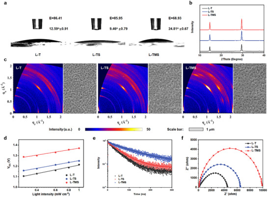
Perovskite film characteristics. a) Contact angle testing with a water droplet on the surface of different ETL substrates. b) XRD patterns of perovskite films. c) GIWAXS patterns and SEM images of the perovskite films deposited on various ETL substrates. d) V OC dependence on light intensities of C‐PSCs. e) TRPL curves of CsPbI2Br films. f) Nyquist plots from EIS measurements of C‐PSCs.
The X‐ray diffraction (XRD) measurements provide direct evidence of the perovskite crystallinity change, as shown in Figure 4b. All perovskite films display peaks at 14.77° and 29.69°, assigned to the (100) and (200) planes of CsPbI2Br, respectively. Notably, the (100) diffraction peak intensities for L─TMS film show significant enhancement compared to those of L─T and L‐TS film, indicating improved crystallinity. Additionally, TA spectra reveal no charge carrier transfer processes at different timescales or additional photobleaching features, confirming the absence of low‐dimensional phases. These observations are in line with XRD patterns, showing exclusively 3D perovskite signatures.[ 44 ]
To further investigate the relationship between film quality and device performance, we conducted grazing incident wide‐angle X‐ray scattering (GIWAXS) of perovskite films. Figure 4c shows 2D GIWAXS patterns of perovskite films on different ETLs. All samples show characteristic scattering rings at 1.0 and 1.5 Å−1, corresponding to the (100) planes. L─TMS perovskite film demonstrates enhanced diffraction intensity at 1.0 Å−1, suggesting preferential crystallographic orientation.[ 45 ] Scanning electron microscopy (SEM) images (Figure 4c) were collected to reveal the morphological change of the perovskite films. While L─TS and L─T perovskite films show comparable crystal sizes, L─TMS films exhibit more faceted rectangular platelets, indicative of oriented crystallization. The crystal size of the film on L─TMS slightly increases, which is in favor of decreasing defects and thus a more unhindered charge diffusion/transfer.
Carrier recombination dynamics were analyzed through the relationship between V OC and the incident light intensity (I). As shown in Figure 4d, the intensity‐dependent slope decreased from 2.03 kT q−1 (L─T) to 1.82 kT q−1 (L─TS) and 1.63 kT q−1 (L─TMS). The reduced slope implies lower non‐radiative recombination caused by trap assistance, consistent with TA measurements. Figure S8 (Supporting Information) shows FFloss between the Shockley–Queisser limit (FFSQ) and the measured FF from J–V curves. The results suggest that the enhanced V OC and FF come from both the suppressed nonradiative recombination and boosted charge transport.[ 46 ]
Figure S9a (Supporting Information) presents the geometry of the PL measurements, in which the 532 nm incident excitation light with the penetration length of 80 nm is from the perovskite side. As shown in Figure S9b (Supporting Information), the intensity of PL peak increases for the L─TMS films, which accounts in suppressed defect recombination in perovskite. TRPL (excitation wavelength of 532 nm from the perovskite side) spectra of perovskite films are shown in Figure 4e. The calculated carrier life prolongs from 41.56 (L─T) to 46.36 (L─TS) and 74.86 ns (L─TMS, summarized in Table S5, Supporting Information). The extended lifetime indicates a lower defect density (e.g., undercoordinated Pb2⁺) for L─TMS films, inhibiting nonradiative recombination and benefiting in improving device performance. Electron‐only devices (FTO/ETLs/perovskite/PCBM/BCP/Ag) were prepared to further prove the reduced trap density in the perovskite films. The trap‐filled limit voltage (V TFL) in Figure S10 (Supporting Information) exhibits a decreased from 0.58 V for L─T device and 0.43 V for L─TS devices to 0.32 V for L─TMS device, suggesting the low defect density from the high‐quality perovskite film. The reduced leakage current (Figure S11, Supporting Information) in the L─TMS devices suggests diminished charge shunting pathways and suppression of charge recombination. The steep slope in the forward bias region suggests low series resistance and efficient charge transport, accounting for the improved V OC and FF. These results are consistent with the decreased series resistance (R S) and increased recombination resistance (R REC) fitted from the electrochemical impedance spectroscopy (EIS) measurements (Figure 4f). Strengthening interfacial adhesion and efficient interfacial passivation improve physical contact and decrease interfacial physical defects. These effects as well as optimized perovskite crystallization enhance electron extraction, reduce charge accumulation at the interface, and decrease carrier recombination (both monomolecular and bimolecular recombination), thus leading to dramatic enhancement in device efficiency and stability.
3. Conclusion
We demonstrate carbon‐based CsPbI2Br HTL‐free planar PSCs with a record V OC of 1.41 V and a high PCE of 17.42%. This breakthrough was realized through a gradient‐arranged electron energy level strategy, which synergistically optimizes electron extraction while suppresses long‐range electron diffusion toward the back electrode. This engineered L─TMS gradient electron conductor enables rapid extraction of photogenerated electrons and efficient carrier separation, thereby significantly suppressing back‐contact recombination. Our work establishes a pioneering strategy for carrier management in HTL‐free C‐PSCs, offering a facile and scalable technique for low‐cost perovskite photovoltaics with industrial compatibility.
Conflict of Interest
The authors declare no conflict of interest.
Author Contributions
Z.L., X.X., and Z.A. contributed equally to this work. G.L., Z.R., and K.L. conceived the idea and supervised the project. Z.L. and X.X. performed the experiments and analyzed the data. Z.A. performed device simulation and analyzed the data. H.L. performed GIWAXS under the supervision of X.L. Q.W. performed transient absorption under the supervision of M.L. T.Z., Y.H., J.X., and R.M. contributed to the data analysis. Z.R., K.L., and Z.L. wrote and G.L. finalized the manuscript. All authors discussed the results and commented on the manuscript.
Supporting information
Supporting Information
Acknowledgements
This work was supported by the Research Grants Council of Hong Kong (Project Nos. 15307922, C7018‐20G, and C4005−22Y), RGC Senior Research Fellowship Scheme (SRFS2223‐5S01); the Hong Kong Polytechnic University: Sir Sze‐yuen Chung Endowed Professorship Fund (8‐8480), RISE (Q‐CDBK), PRI (Q‐CD7X), Hong Kong Innovation and Technology Fund (ITF‐TCFS GHP/380/22GD), and Guangdong‐Hong Kong‐Macao Joint Laboratory for Photonic‐Thermal‐Electrical Energy Materials and Devices (GDSTC No. 2019B121205001), and National Natural Science Foundation of China (52403250). Z. R. acknowledges financial support from the Start‐up Fund for RAPs under the Strategic Hiring Scheme (1‐BD1H), RI‐iWEAR Strategic Supporting Scheme (1‐CD94), and Innovation and Technology Fund ITF‐ITSP (ITS/184/23) for this work.
Li Z., Xie X., Ai Z., Han Y., Zhu T., Ma R., Liu H., Lu X., Wei Q., Li M., Xiao J., Liu K., Ren Z., Li G., Electron Extraction Optimization for Carbon‐Based Hole‐Conductor‐Free Perovskite Photovoltaics With Record 1.41 V V OC . Adv. Mater. 2025, 37, 2502436. 10.1002/adma.202502436
Contributor Information
Kuan Liu, Email: kuan-lk.liu@polyu.edu.hk.
Zhiwei Ren, Email: zhiweipv.ren@polyu.edu.hk.
Gang Li, Email: gang.w.li@polyu.edu.hk.
Data Availability Statement
The data that support the findings of this study are available from the corresponding author upon reasonable request.
References
- 1. Luo C., Zheng G., Gao F., Wang X., Zhan C., Gao X., Zhao Q., Nat. Photon. 2023, 17, 856. [Google Scholar]
- 2. Domanski K., Alharbi E., Hagfeldt A., Grätzel M., Tress W., Nat. Energy. 2018, 3, 61. [Google Scholar]
- 3. Lim J., Park N. G., Il Seok S., Saliba M., Energy Environ. Sci. 2024, 17, 4390. [DOI] [PMC free article] [PubMed] [Google Scholar]
- 4. Yang G., Ren Z., Liu K., Qin M., Deng W., Zhang H., Wang H., Liang J., Ye F., Liang Q., Yin H., Chen Y., Zhuang Y., Li S., Gao B., Wang J., Shi T., Wang X., Lu X., Wu H., Hou J., Lei D., So S. K., Yang Y., Fang G., Li G., Nat. Photon. 2021, 15, 681. [Google Scholar]
- 5. Chen H., Liu C., Xu J., Maxwell A., Zhou W., Yang Y., Zhou Q., Bati A. S., Wan H., Wang Z., Zeng L., Wang J., Serles P., Liu Y., Teale S., Liu Y., Saidaminov M., Li M., Rolston N., Hoogland S., Filleter T., Kanatzidis M., Chen B., Ning Z., Sargent E., Science 2024, 384, 189. [DOI] [PubMed] [Google Scholar]
- 6. Zhou J., Tan L., Liu Y., Li H., Liu X., Li M., Wang S., Zhang Y., Jiang C., Hua R., Tress W., Meloni S., Yi C., Joule 2024, 8, 1691. [Google Scholar]
- 7. Tang H., Shen Z., Shen Y., Yan G., Wang Y., Han Q., Han L., Science 2024, 383, 1236. [DOI] [PubMed] [Google Scholar]
- 8. Li X., Fu S., Zhang W., Ke S., Song W., Fang J., Sci. Adv. 2020, 6, 1580. [DOI] [PMC free article] [PubMed] [Google Scholar]
- 9. Liu A., Li X., Zhang W., Yang H., Guo X., Lu C., Yuan H., Ou‐Yang W., Fang J., Adv. Funct. Mater. 2023, 34, 2307310. [Google Scholar]
- 10. Li G., Gao X., Adv. Mater. 2020, 32, 1806478. [DOI] [PubMed] [Google Scholar]
- 11. Raza H., Imran T., Gao Y., Azeem M., Younis M., Wang J., Liu S., Yang Z., Liu Z., Chen W., Energy Environ. Sci. 2024, 17, 1819. [Google Scholar]
- 12. Bogachuk D., Zouhair S., Wojciechowski K., Yang B., Babu V., Wagner L., Xu B., Lim J., Mastroianni S., Pettersson H., Hagfeldt A., Hinsch A., Energy Environ. Sci. 2020, 13, 3880. [Google Scholar]
- 13. Pradid P., Sanglee K., Thongprong N., Chuangchote S., Materials 2021, 14, 5989. [DOI] [PMC free article] [PubMed] [Google Scholar]
- 14. Yu Y., Hoang M. T., Yang Y., Wang H., Carbon 2023, 205, 270. [Google Scholar]
- 15. Luo Q., Ma H., Hou Q., Li Y., Ren J., Dai X., Yao Z., Zhou Y., Xiang L., Du H., He H., Wang N., Jiang K., Lin H., Zhang H., Guo Z., Adv. Funct. Mater. 2018, 28, 1706777. [Google Scholar]
- 16. Han C., Du J., Liu Z., Gao Q., Chen X., Xiang J., Xiao X., Cheng Y., Chen K., Xia M., Liu J., Yang L. M., Zhou Y., Mei A., Han H., Adv. Funct. Mater. 2024, 34, 2408686. [Google Scholar]
- 17. Song J., Xie H., Lim E. L., Hagfeldt A., Bi D., Adv. Energy Mater. 2022, 12, 2201854. [Google Scholar]
- 18. Ozturk T., Akman E., Shalan A. E., Akin S., Nano Energy 2021, 87, 106157. [Google Scholar]
- 19. Li M., Wang S., Ma X., Long R., Wu J., Xiao M., Fu J., Jiang Z., Chen G., Jiang Y., Hu J., Joule 2023, 7, 2595. [Google Scholar]
- 20. Shan S., Xu C., Wu H., Niu B., Fu W., Zuo L., Chen H., Adv. Energy Mater. 2022, 13, 2203682. [Google Scholar]
- 21. Jeong M. J., Jeon S. W., Kim S. Y., Noh J. H., Adv. Energy Mater. 2023, 13, 2300698. [Google Scholar]
- 22. Li M., Ma X., Fu J., Wang S., Wu J., Long R., Hu J., Energy Environ. Sci. 2024, 17, 5513. [Google Scholar]
- 23. Zhang G., Xie P., Huang Z., Yang Z., Pan Z., Fang Y., Rao H., Zhong X., Adv. Funct. Mater. 2021, 31, 2011187. [Google Scholar]
- 24. Lim E. L., Yang J., Wei Z., Energy Environ. Sci. 2023, 16, 862. [Google Scholar]
- 25. Li M., Gong X., Wang S., Li L., Fu J., Wu J., Tan Z., Hu J., Angew. Chem. Int. Ed. Engl. 2024, 63, 202318591. [DOI] [PubMed] [Google Scholar]
- 26. Li M., Shao J., Jiang Y., Qiu F., Wang S., Zhang J., Han G., Tang J., Wang F., Wei Z., Yi Y., Zhong Y., Hu J., Angew. Chem. Int. Ed. Engl. 2021, 60, 16388. [DOI] [PubMed] [Google Scholar]
- 27. Jiang S., Bai Y., Xu Z., Wang F., Xia L., Yang Y., Li C., Tan Z., Small Methods. 2022, 6, 2200624. [DOI] [PubMed] [Google Scholar]
- 28. Liu C., He J., Wu M., Wu Y., Du P., Fan L., Zhang Q., Wang D., Zhang T., Sol. RRL 2020, 4, 2000016. [Google Scholar]
- 29. Han Y., Fu J., Ren Z., Yu J., Liang Q., Xu Z., Xie X., Li D., Ma R., Cao M., Sun Y., Yang C., He J., Chang X., Liu K., Fong P., Huang J., Liu H., Liu Z., Xu D., Cheng L., Zhang J., Yang G., Lu X., Zhu Y., Tai Q., Lin Q., Hu H., Yang Y., Li G., Nat. Energy 2025, 1. [Google Scholar]
- 30. Ren Z., Liu K., Hu H., Guo X., Gao Y., Fong P. W. K., Liang Q., Tang H., Huang J., Zhang H., Qin M., Cui L., Chandran H. T., Shen D., Lo M., Ng A., Surya C., Shao M., Lee C., Lu X., Laquai F., Zhu Y., Li G., Light Sci. Appl. 2021, 10, 239. [DOI] [PMC free article] [PubMed] [Google Scholar]
- 31. Elumalai N., Uddin A., Sol. Energy Mater. Sol. Cells. 2016, 157, 476. [Google Scholar]
- 32. Wang S., Li M., Zhang Y., Jiang Y., Xu L., Wang F., Hu J., Energy Environ. Sci. 2023, 16, 2572. [Google Scholar]
- 33. Aydin E., Bastiani M. D., Wolf S. D., Adv. Mater. 2019, 31, 1900428. [DOI] [PubMed] [Google Scholar]
- 34. Li C., Dogan S., Li Y., Zhang H., Tang S., Yuan Z., Liang L., Zhang Z., Wang Y., Liu C., Yang Y., Ince M., Gao P., Adv. Energy Mater. 2024, 15, 2402856. [Google Scholar]
- 35. Ding C., Zhang Y., Liu F., Kitabatake Y., Hayase S., Toyoda T., Yoshino K., Minemoto T., Katayama K., Shen Q., Nano Energy. 2018, 53, 17. [Google Scholar]
- 36. Chen P., Bai Y., Wang L., Small Struct. 2021, 2, 2000050. [Google Scholar]
- 37. Jung E. H., Chen B., Bertens K., Vafaie M., Teale S., Proppe A., Hou Y., Zhu T., Zheng C., Sargent E. H., ACS Energy Letters. 2020, 5, 2796. [Google Scholar]
- 38. Lu Y., Shih M. C., Tan S., Grotevent M., Wang L., Zhu H., Zhang R., Lee J., Lee J., Bulovic V., Bawendi M., Adv. Mater. 2023, 35, 2304168. [DOI] [PubMed] [Google Scholar]
- 39. Wang W., Zhao D., Zhang F., Li L., Du M., Wang C., Yu Y., Huang Q., Zhang M., Li L., Miao J., Lou Z., Shen G., Fang Y., Yan Y., Adv. Funct. Mater. 2017, 27, 1703953. [Google Scholar]
- 40. Liu J., Chen X., Chen K., Tian W., Sheng Y., She B., Jiang Y., Zhang D., Liu Y., Qi J., Chen K., Science 2024, 383, 1198. [DOI] [PubMed] [Google Scholar]
- 41. Wu W., Chen D., Li F., Pascoe A., Cheng Y., Caruso R., Nano Energy. 2017, 32, 187. [Google Scholar]
- 42. Li Z., Wei Q., Wang Y., Tao C., Zou Y., Liu X., Li Z., Wu Z., Li M., Guo W., Li G., Xu W., Gao F., Nat. Commun. 2025, 16, 927. [DOI] [PMC free article] [PubMed] [Google Scholar]
- 43. Yang S., Park J., Jeong S., Cho Y., Jeong M., Oh J., Lee S., Park J., Yoon S., Yang C., ACS App. Mater. Interfaces. 2023, 15, 39636. [DOI] [PubMed] [Google Scholar]
- 44. Yang S., Wen J., Liu Z., Che Y., Xu J., Wang J., Xu D., Yuan N., Ding J., Duan Y., Liu S., Adv. Energy Mater. 2022, 12, 2103019. [Google Scholar]
- 45. Tian J., Xue Q., Tang X., Chen Y., Li N., Hu Z., Shi T., Wang X., Huang F., Brabec C. J., Yip H. L., Cao Y., Adv. Mater. 2019, 31, 1901152. [DOI] [PubMed] [Google Scholar]
- 46. Liang Q., Liu K., Sun M., Ren Z., Fong P. W. K., Huang J., Qin M., Wu Z., Shen D., Lee C., Hao J., Lu X., Huang B., Li G., Adv. Mater. 2022, 34, 2200276. [DOI] [PubMed] [Google Scholar]
Associated Data
This section collects any data citations, data availability statements, or supplementary materials included in this article.
Supplementary Materials
Supporting Information
Data Availability Statement
The data that support the findings of this study are available from the corresponding author upon reasonable request.