

Abstract
The discovery and synthesis of atomically precise low‐dimensional inorganic materials have led to numerous unusual structural motifs and nascent physical properties. However, access to low‐dimensional van der Waals (vdW)‐bound analogs of bulk crystals is often limited by chemical considerations arising from structural factors like atomic radii, bonding or coordination, and electronegativity. Using single‐walled carbon nanotubes (SWCNTs) as confinement templates, we demonstrate the synthesis of a short‐wave infrared‐absorbing quasi‐1D (q‐1D) chain polymorph of Sb2Te3 ([Sb4Te6]n) that is structurally and electronically distinct from its 2D counterpart. It is found that the q‐1D chain polymorph has both three‐ and five‐coordinate Sb atoms covalently bonded to Te and is thermodynamically stabilized by the electrostatic interaction between the encapsulated chain and the model SWCNT. The complementary experimental and computational results demonstrate the synthetic advantage of vdW nanotube confinement in the discovery of low‐dimensional polytypes with drastically altered physical properties and potential applications in energy conversion processes.
Keywords: 1D van der Waals crystals, carbon nanotube, heterostructure, pnictogen chalcogenide, polymorphism, semiconductor
The precise synthesis of 1D materials has enabled the discovery of physical properties only accessible in length scales close to the atomic scale. Herein, it is demonstrated that encapsulation within single‐walled carbon nanotubes with matching diameters leads to a stoichiometric quasi‐1D van der Waals polymorph of a 2D pnictogen chalcogenide, Sb2Te3, with a blue‐shifted band gap in the short‐wave infrared regime.

1. Introduction
Advances in the precision synthesis of inorganic 1D materials have enabled the discovery of unprecedented properties and physical states only accessible in length scales close to the atomic scale.[ 1 , 2 , 3 , 4 , 5 ] Crystals that possess underlying 1D or quasi‐1D (q‐1D) atomic ordering[ 6 ] can readily form 1D morphologies such as nanowires and nanoribbons that approach the atomic scale via top‐down exfoliation of bulk crystals[ 7 , 8 ] or bottom‐up vapor phase synthesis.[ 9 , 10 ] However, directing the synthesis of atomically precise 1D chain or nanowire analogs from higher dimensional 2D or 3D crystals is far from trivial. Often, these synthetic approaches require distinct and complex chemical transformations such as nanoparticle‐directed vapor‐liquid‐solid (VLS) or vapor‐solid (VS) growth,[ 11 , 12 , 13 , 14 ] ligand capping,[ 15 , 16 ] and even substrate‐directed growth[ 17 ] to define nanowires with high precision. Despite these strategies, the 1D structures accessible through such routes are usually limited to the nanoscale and hardly approach the atomic scale where many of the sought‐after properties emerge. Alternatively, access to atomically precise 1D structures that are stable under ambient conditions can be reliably achieved through nanotube encapsulation.[ 18 , 19 , 20 , 21 ] Carbon nanotubes (CNTs)[ 22 ] and boron‐nitride nanotubes (BNNTs)[ 23 ] are, by nature, atomically well‐defined, follow a specific set of size‐dependent chiral indices (n,m), can reach ultrathin diameters (<1 nm), and extend across long length scales (>µm).[ 24 ] Owing to inert vdW surfaces, these nanotubes can act as templates that pre‐define the diameter of the structure grown within, resulting in uniform widths with minimal chemical perturbation.[ 21 , 25 ]
Among the low‐dimensional solids sought for their 1D character, pnictogen chalcogenides (Pn2Ch3; Pn = Sb, Bi and Ch = S, Se, Te) stand out as a rich class in structure, dimensionality, and nascent physical properties (Figure 1 ).[ 26 ] The structural and chemical diversity of this class is apparent in the co‐existence of two structure types. Phases consisting of lighter elements such as Sb2S3,[ 27 ] Sb2Se3,[ 28 ] and Bi2S3 [29] crystallize as q‐1D vdW ribbon‐like chains with rectangular [(Sb or Bi)4Ch6]n (Ch = S, Se) chain cross–sections containing both a pentavalent pnictogen core and a trivalent terminal pnictogen. Alternatively, the layered rhombohedral/hexagonal 2D vdW crystals of Sb2Te3,[ 30 ] Bi2Se3,[ 31 ] and Bi2Te3 [32] have only one type of pnictogen environment characterized by hexavalent coordination to chalcogen atoms along the covalent 2D quintuple layers held together by weak non‐covalent interactions (Figure 1A). Both structure types offer a host of physical properties, with the lighter q‐1D materials being employed in earth‐abundant nanoscale photovoltaics,[ 33 , 34 , 35 , 36 ] phase change materials (PCMs) for optical switching and non‐volatile data storage,[ 37 , 38 ] or as excitonic 1D nanocrystals,[ 39 ] while the heavier 2D phases are sought‐after for their high thermoelectric figures of merit,[ 40 , 41 , 42 ] robust topologically protected states,[ 43 , 44 ] as well as for their PCM behavior.[ 45 , 46 ] The co‐existence of the dimensionally distinct q‐1D and 2D structure types in pnictogen chalcogenides is intriguing as—despite identical electron counts—these low‐dimensional crystals manifest structures with distinctly varied local chemical environments that relate to their dimensionalities.
Figure 1.

Crystalline phases of the Sb2Ch3 (Ch = S, Se, Te) family. A) Crystal structures of q‐1D Sb2S3, q‐1D Sb2Se3, and 2D Sb2Te3. B) Synthetic and materials processing routes to access nanoscale analogs of the 2D Sb2Te3 polymorph and conceptual depiction of the q‐1D [Sb4Te6]n chain encapsulated within a SWCNT presented in this study. On the right of the red box are the crystallographic axes and orientation with respect to the parent 2D Sb2Te3 phase while on the left are the x, y, and z axes used in the computational results in this study.
Because of the size and dimensional confinement on physical states of these materials, efforts have been made to control the size and dimensionality of pnictogen chalcogenides including Sb2Te3. These include the creation of ultrathin 2D nanosheets accessible from both top‐down exfoliation[ 47 , 48 ] (Figure S1, Supporting Information) and chemically directed bottom‐up vapor phase growth as well as 1D nanowires accessible from catalyst‐directed vapor phase synthesis (Figure 1B).[ 14 ] While these routes enable the control of the nanoscale dimensionality of the native structure, synthetic strategies towards the q‐1D vdW crystalline polytype of Sb2Te3 have remained elusive. Thus, synthetically bridging the q‐1D to 2D gap in stoichiometric Pn2Ch3 crystals requires a level of atomic precision like vdW nanotube encapsulation.
Herein, we report the discovery of short‐wavelength infrared (SWIR)‐absorbing Sb2Te3 chains ([Sb4Te6]n) bearing the q‐1D vdW pnictogen chalcogenide polytype structure through SWCNT encapsulation. The structure and composition of the chains were established via high‐resolution transmission electron microscopy (HRTEM), Cs‐corrected scanning transmission electron microscopy (STEM), energy dispersive X‐ray spectroscopy (EDS), electron energy loss spectroscopy (EELS), and X‐ray photoelectron spectroscopy (XPS). Density Functional Theory (DFT) calculations were used to determine the lowest‐energy structure of the [Sb4Te6]n chain, featuring pentavalent and trivalent Sb, and its corresponding band structure. Both experimental and theoretical efforts establish the q‐1D vdW polytype structure of encapsulated [Sb4Te6]n chains to be isostructural to Sb2S3, Sb2Se3, and Bi2S3. To our knowledge, this represents the first example of the bridging of a structural gap of this type between dimensionally distinct parent crystalline phases. These results expand the range of accessible vdW Pn2Ch3 crystals with atomic precision, demonstrating a robust synthetic strategy to access low‐dimensional polytypes with vastly different properties compared to their higher‐dimensional counterparts.
2. Results and Discussion
2.1. Confined Synthesis of q‐1D Sb2Te3 Within SWCNTs
We encapsulated Sb2Te3 within SWCNTs using melt‐phase crystalline precursors of the 2D phase that are driven into open‐ended nanotubes via capillary action.[ 49 ] SWCNTs were annealed and oxidized at 420 °C in air to selectively open the tube ends and were subsequently combined with a large excess of pre‐synthesized Sb2Te3 bulk material. This mixture was kept in a sealed vacuum ampoule at 650 °C, above the melting point of Sb2Te3. Successful filling of SWCNTs with pure Sb2Te3 depended on the purity of the Te precursor used to synthesize the Sb2Te3 precursor, as was observed when starting from Te powders with surface TeO2. The persistence of this surface oxide results in unreacted Te with the bulk Sb2Te3 and a mixture of nanotubes filled with Te and Sb2Te3 (Figures S2 and S3, Supporting Information). Instead, by using unoxidized Te, we were able to synthesize pure Sb2Te3 precursors with no trace of unreacted Te, confirmed by powder X‐ray diffraction (PXRD) (Figure S2, Supporting Information). The use of pure Sb2Te3 precursors resulted in the successful synthesis of Sb2Te3 chains within SWCNTs. The elemental composition of encapsulated Sb2Te3 chains is corroborated by both EDS and XPS results (Figures S4, S7, and S8, Supporting Information). These chains of interest are denoted, from hereon, as [Sb4Te6]n@SWCNT for consistency.
We elucidated the structure of the [Sb4Te6]n@SWCNTs by combining the structure observed from HRTEM with the energy‐minimized structure using DFT (Figure 2 ). Here, it was evident that the encapsulated Sb2Te3 contrasted greatly from either the helical structure of elemental Te50 or the 2D hexagonal motif of bulk Sb2Te3.[ 30 ] Instead, the Sb2Te3 encapsulated within SWCNTs displayed an extended 1D chain structure of [Sb4Te6]n with three atom‐wide columns staggered in a zig‐zag pattern (Figure 2A). This motif is reminiscent of the q‐1D sub‐structure of Sb2S3 or Sb2Se3 observed both in the bulk crystal structures[ 27 , 28 ] and when encapsulated as chains within SWCNTs.[ 25 , 51 ] The covalent axis of this chain shows a systematic spacing of 2.1 Å, closely matching the (110) spacing of the native 2D structure (2.132 Å). This preferred 1D growth direction is consistent with nanoparticle‐directed CVD‐grown nanowires, which typically form nanoribbons that lay flat along the [001] zone axis while retaining the underlying 2D hexagonal structure with exposed vdW facets.[ 14 ] Yet, rather than displaying the dominant [001] axis, the encapsulated chains indexed to an approximate [5‐51] zone axis of the bulk Sb2Te3 rhombohedral crystal. Intriguingly, hypothetically truncating the bulk structure with planes normal to the [5‐51] direction to form a chain with the same width as the experimentally observed chain structure resulted in an [Sb4Te6]n chain resembling the chains that constitute the lighter Sb2Ch3 analogs (Figure 2B,E). These HRTEM results suggest that a q‐1D [Sb4Te6]n chain polytype of Sb2Te3, distinct from the 2D rhombohedral phase, was apparent upon encapsulation.
Figure 2.

Electron microscopy and structure of Sb2Te3@SWCNT. A) Experimentally obtained HRTEM of Sb2Te3@SWCNT (left) with FFT of a square region indexing to the [5‐51] zone axis (right). B) Sb2Te3 bulk structure along [5‐51] truncated to an [Sb4Te6]n chain (left) and its cross–section (right). C) Simulated HRTEM images of DFT‐predicted [Sb4Te6]n relaxed within SWCNT(24,0) (top) or SWCNT(21,0) (bottom) with the corresponding simulated diffraction patterns (right). D) DFT‐predicted structures of [Sb4Te6]n relaxed within a SWCNT(24,0) (top) or SWCNT(21,0) (bottom) with the respective cross–sections displaying varying degrees of nanotube distortion (right). E) Bulk 2D Sb2Te3 structure truncated to a [Sb4Te6]n chain. F) Magnified view of the [Sb4Te6]n chain cross–section before relaxation (left) and after relaxation within SWCNT(24,0) (right) highlighting bond distortion and opening from pentavalent to trivalent q‐1D‐type Sb. The Miller indices and orientations correspond to the crystallographic directions of the parent 2D Sb2Te3 structure.
We used DFT calculations to optimize the q‐1D structure in SWCNTs of two sizes: i) a (24,0) 18.8 Å nanotube to directly compare to the experimentally observed 19 Å nanotube and ii) a (21,0) 16.4 Å SWCNT to represent the average diameter of our nanotube source (Tuball; 16 ± 4 Å) (Figure 2C,D), although we note that other (n,m) nanotubes, including chiral nanotubes, also exist within this sample. After geometry optimization, both nanotubes relaxed to an elliptical cross–section with the longest diameter being ≈19 Å in the direction parallel to the [Sb4Te6]n chain (Figure 2D). This indicates that the ribbon‐like chain structure induced an anisotropic structural distortion in both nanotubes, with a more pronounced effect on the smaller (21,0) nanotube (Figure 2D). The anisotropic distortion predicted from DFT is confirmed by Raman spectroscopy, where the lateral G−‐band broadened significantly and asymmetrically (Figure S5 and Table S1, Supporting Information). This nanotube distortion has been previously reported and can result from either internal[ 52 ] or external[ 53 ] vdW pressure. This anisotropic nanotube distortion that flattens the structure may also be the origin of the specific and preferred orientation of the encapsulated chains observed in S/TEM experiments, as wide, ribbon‐like Sb2Se3 chains encapsulated in nanotubes also induced a similar preferred alignment.[ 25 ] The [Sb4Te6]n chain itself is comparable between [Sb4Te6]n@SWCNT(24,0) or [Sb4Te6]n@SWCNT(21,0), with differences in bond length in the range of ≤0.5 Å, which is within the resolution limit of the HRTEM. Thus, it is not discernible which exact nanotube is hosting the [Sb4Te6]n chain from this experiment, as simulated HRTEM images of either the [Sb4Te6]n@SWCNT(24,0) or [Sb4Te6]n@SWCNT(21,0) structures appear virtually identical (Figure 2A,C). Both DFT structures agree well with our experimental assignment of the structure of the [Sb4Te6]n chain.
2.2. Bonding, Stability, and Atomic Structure of [Sb4Te6]n@SWCNT
The DFT‐relaxed structure of [Sb4Te6]n in either (21,0) or (24,0) SWCNT (SWCNT(21,0) and SWCNT(24,0)) shares many structural similarities as the q‐1D structure native to the Sb2S3 and Sb2Se3 phases.[ 27 , 28 ] The peripheral Sb atoms (Te‐bound) in the [Sb4Te6]n chain elongate to form a trivalent Sb site with trigonal pyramidal geometry, while the core Sb atoms retain pentavalent coordination with square pyramidal geometry (Figure 2F). These coordination environments suggest that the 5s electrons of the trigonal pyramidal Sb atoms are expressed as a lone pair, similar to the peripheral Sb atoms in Sb2S3 or Sb2Se3 chains.[ 54 ] This result is complemented by experimental findings in XPS, which show a 0.17 eV decrease in Sb 3d5/2 binding energy peak from 529.12 eV in bulk Sb2Te3 to 528.95 in [Sb4Te6]n@SWCNT, suggesting an increased electron density localized on Sb (Figure S8 and Table S2, Supporting Information).
We also computed the formation energy (E f) of [Sb4Te6]n in SWCNTs using DFT to estimate the likelihood of [Sb4Te6]n encapsulation within SWCNT and assess the thermodynamic stability of the resulting [Sb4Te6]n@SWCNTs. The formation energies of the confined [Sb4Te6]n chain in a SWCNT(21,0) and SWCNT(24,0) are E f = 1.33 and E f = −1.26 eV, respectively. This indicates a strong thermodynamic driving force for [Sb4Te6]n to be encapsulated in a larger SWCNT(24,0). The encapsulation by a smaller SWCNT(21,0) at equilibrium appears energetically unfavorable based on the positive formation energy predicted, highlighting that the diameter of SWCNTs should be larger than 16 Å to favor encapsulation of this specific q‐1D [Sb4Te6]n structure type. Thus, it is more likely for the experimental structure to be in SWCNTs with diameters >16 Å, which is within the range of SWCNTs employed in this study. From previous reports,[ 55 ] other q‐1D Sb2Te3 structures form within smaller SWCNTs, further truncated and distinct from the ideal Sb2S3‐like [Sb4Te6]n chain structure that we reported herein, although these structures amorphized under the electron beam, likely due to the instability of Sb and Te with unsatisfied valencies (Figure S11, Supporting Information). Across several synthesis batches, these amorphous wires (or those that appeared metastable and rapidly amorphized) accounted for approximately half of the wires observed, while the crystalline [Sb4Te6]n occupied over one‐third of the nanotubes. The remainder of the nanotubes were found to be empty. These empty nanotubes had no size dependence, meaning they likely did not open at the ends during annealing and therefore could not fill. We predict that using a narrower size distribution of SWCNTs centered around approximately 19 Å could increase the amount of [Sb4Te6]n present in the sample relative to the other material. The predicted adhesive energies (E adh) between [Sb4Te6]n and SWCNTs have negative values: E adh = −1.28 and −3.89 eV for the SWCNT(21,0) and SWCNT(24,0), respectively. These values indicate an energetically favorable vdW and electrostatic interaction between the encapsulated [Sb4Te6]n chain and the SWCNT, where the SWCNTs help stabilize the electronic structure of the q‐1D polymorph of Sb2Te3.
We performed Cs‐corrected high‐angle annular dark‐field STEM (HAADF‐STEM) along with EELS to better establish the structure and composition of the encapsulated [Sb4Te6]n chains with higher spatial resolution (Figure 3 ; Figures S9 and S10, Supporting Information). Here, the heavier Sb and Te atoms are significantly better resolved compared to HRTEM. Using [Sb4Te6]n@SWCNT(24,0) as a model due to its calculated stability, we compared the experimental HAADF‐STEM image to the energetically relaxed atomic model structure from DFT (Figure 3). The simulated image matched the experimental micrograph to a remarkable degree of similarity (Figure 3A). To assess similarities between the experimental structure and the atomic model, we took intensity profiles from different regions of both the experimental and simulated STEM images (Figure 3B,D). Both Sb(1)‐Sb(1) / Te(1)‐Te(1) distances (Figure 3D; II and III) and Sb(1)‐Sb(2) / Te(1)‐Te(2) distances (Figure 3D; IV and V) were exceptionally close to the proposed model based on the intensity plots. Additionally, in the atomic model of [Sb4Te6]n, the projection includes both single‐atom thick columns of Te at the edges and two‐atom thick columns of Sb and Te along the center. Due to their similar atomic numbers (Z Sb = 51 and Z Te = 52), scattering from Sb and Te is virtually identical and is suggestive that intensities from the Sb‐Te columns in the center should be approximately twice that of the single Te atom at the edges. This is experimentally observed in Figure 3D, as plots I, IV, and V show two distinct peak heights corresponding to single and double atom thickness, while plot II is roughly double plot III in intensity as expected.
Figure 3.

HAADF‐STEM and EELS of [Sb4Te6]n@SWCNT. A) HAADF‐STEM of [Sb4Te6]n@SWCNT with DFT‐predicted structure within a (24,0) nanotube (left), a simulated image (center), and a real image (right). B) Additional HAADF‐STEM image of [Sb4Te6]n@SWCNT distinct from the wire shown in A with highlighted regions corresponding to intensity profiles. C) EELS maps of an [Sb4Te6]n@SWCNT bundle with a 2:3 ratio of Sb to Te. D) Intensity profiles from B contrasted with intensity profiles of the simulated HAADF‐STEM image.
No other structure that preserves the native crystalline symmetry truncated from the parent bulk Sb2Te3 fit the experimental data while remaining stoichiometric and charge balanced (Figure S13, Supporting Information), although we found that [Sb5Te7]n +@SWCNTs also provided an alternative phase fit to some of the regions in our STEM images as well as the [Sb4Te6]n phase (Figure S14, Supporting Information). This structure, which we do not discount as a possible phase that could exist within the SWCNT, minimizes charge relative to other truncations of the bulk structure (Figure S13, Supporting Information), with only a +1 overall charge. The region selected also varied, to some extent, due to instrumental noise, with some regions of the wire in Figure 3B matching more closely to [Sb5Te7]n + and some to [Sb4Te6]n. Additionally, the two atoms along the core of the wire in Figure 3A were also observed to be artificially inflated in intensity due to an overlapping amorphous wire (Figure S14, Supporting Information). Additional limitations of this intensity analysis are further discussed in the supporting information. Although carbon nanotubes can support charged species within,[ 56 ] EELS mapping of the [Sb4Te6]n@SWCNTs also corroborates a 2:3 ratio of Sb:Te localized within the nanotubes (Figure 3C). As such, taken together, EDS, EELs, and XPS all point toward [Sb4Te6]n favored over [Sb5Te7]n +@SWCNT. Despite this, these are each ensemble measurements, meaning local areas could fluctuate in composition and may still result in an overall 2:3 ratio. Based on our measurements, we cannot rule out an off‐stoichiometric structure existing within some nanotubes, though we find the likelihood of a 2:3 stoichiometric [Sb4Te6]n chain forming to be greater than other phases based on charge balance and ensemble measurements. Direct observation of the structure by HAADF‐STEM and its persistent stability compared to thinner structures (Figure S11, Supporting Information) provides strong evidence for the q‐1D [Sb4Te6]n pnictogen chalcogenide polytype of Sb2Te3 isolated within SWCNTs.
2.3. Optical and Electronic Properties of [Sb4Te6]n@SWCNT
Following the successful synthesis of [Sb4Te6]n@SWCNT, we probed the optical and electronic properties of the encapsulated [Sb4Te6]n using spectroscopic and DFT approaches. From Fourier‐transformed infrared (FTIR) spectroscopy, an absorption peak centered at 0.67 eV was apparent in the SWIR region, which we attribute to the [Sb4Te6]n chain (Figure 4A). Compared to the absorption profiles of isostructural [Sb4S6]n and [Sb4Se6]n chains within SWCNTs,[ 25 , 51 ] this peak is consistent with the closing of the band gap (E g) from the visible to the SWIR range expected from the significantly lower degree of Sb—Ch (Ch = S, Se, Te) orbital overlap in the Te‐based [Sb4Ch6]n analog. It also agrees well with the estimated bandgap of 0.54 eV, based on our DFT calculations of the [Sb4Te6]n chain encapsulated within SWCNT(24,0). We do not expect other (n,m) nanotubes to have a significant impact on the electronic properties of the [Sb4Te6]n chain, although we do not discount the contribution of these other indexed nanotubes to the ensemble measurements taken. The valence band of the [Sb4Te6]n predominantly consists of Te‐5p orbitals, while the conduction band results from the overlap between the Te 5p and Sb 5p orbitals (Figure 4B). The confined [Sb4Te6]n chain is predicted to be an indirect band gap phase which—as expected from the dimensionality and the structural distinction of the q‐1D polymorph—is significantly blue‐shifted from the bandgap of the bulk 2D crystal (E g,exp'l = 0.21 eV[ 57 ] and E g,DFT = 0.13 eV) (Figure S15, Supporting Information). Upon encapsulation, the Fermi level of the [Sb4Te6]n chain also shifts upward, nearing the conduction band minimum (CBM), indicating charge transfer from the SWCNT to the encapsulated [Sb4Te6]n to achieve thermodynamic stability. When coupled with the [Sb4Te6]n chain, the electronic structure of the SWCNT remains metallic despite the appearance of slight anisotropic structural distortions compared to an empty SWCNT(24,0) (Figure S16, Supporting Information). The valence band maximum (VBM) corresponding to SWCNT states in [Sb4Te6]n@SWCNT is also within 0.1 eV to the CBM of the confined [Sb4Te6]n chain states, indicative of electron transfer from the SWCNT to the unoccupied states of [Sb4Te6]n across the interface. This distinct feature would promote efficient charge‐carrier separation and is suggestive of enhanced carrier lifetimes.[ 58 , 59 ]
Figure 4.
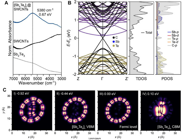
Optical and electronic nature of [Sb4Te6]n@SWCNT. A) Room temperature FTIR absorption spectra of the 2D Sb2Te3, SWCNTs, and [Sb4Te6]n@SWCNTs in the SWIR range. B) Calculated band structure, the total density of states (TDOS), and the projected density of states (PDOS) of [Sb4Te6]n@SWCNT(24,0) from DFT (C) Calculated charge‐density maps of [Sb4Te6]n@SWCNT(24,0) projected on the cross‐sectional planes along the nanotube length at energies relative to the Fermi level. Light contrast regions indicate relatively high electron density, while the dark contrast regions indicate low electron density.
We analyzed the spatial distribution of the electron density at specific energy levels to understand the chemical bonding nature of [Sb4Te6]n when encapsulated within SWCNT(24,0) (Figure 4C). The light‐contrast regions indicate areas of higher electron densities, corresponding to both bonding and lone pair electrons. From these maps, the charge density in the valence band is predominantly localized in the SWCNT, which primarily consists of out‐of‐plane π‐covalent character through the hybridization of pz orbitals of carbon atoms. Below the Fermi level in Figure 4C‐I,II), electrons are delocalized over both [Sb4Te6]n and SWCNT, owing to the mixing of the electronic states between the two phases upon interfacing (e.g., at −0.92 and −0.44 eV; Figure 4C‐I,II). At the Fermi level (Figure 4C‐III), however, the electron density is spatially localized distinctly in the SWCNT, suggesting the persistent metallic character of the nanotube and the resulting [Sb4Te6]n@SWCNT. At the conduction band (Figure 4C‐IV), the electron density is mostly localized at the [Sb4Te6]n chain, and the electronic character is dominated by the hybridization of Sb and Te p‐orbital states. We expect these orbitals to play a dominant role in determining the electronic properties of [Sb4Te6]n@SWCNT, such as charge carrier mobility.
We further inspected the redistribution of electron density in the [Sb4Te6]n chain upon encapsulation within the SWCNT(24,0) by calculating the charge density difference between the isolated [Sb4Te6]n chain and its encapsulated phase (Figure 5A). From DFT calculations, we find that electron charge transfer likely occurs from the SWCNT to [Sb4Te6]n through the peripheral Te atoms that are oriented toward the nanotube wall. This finding is consistent with our discussion regarding the upward shift in the Fermi level upon encapsulation. Intriguingly, the charge transfer process results in a slight polarization of the two phases, where SWCNT becomes more positively charged and the [Sb4Te6]n becomes more negatively charged. Such charge transfer consequently stabilizes the encapsulated structure via electrostatic interactions. We also assessed the band alignment between the [Sb4Te6]n chain and this specific SWCNT(24,0), using the local density of states along the different cross‐sectional views (Figure 5B,C) and estimated the work function to be 4.32 eV (Figure 5D,E). This specific value will likely change depending on whether the SWCNT is metallic or semiconducting, as the DOS will change. There is a greater extent of electron density overlap between the chain and the nanotube along the longer axis (y) compared to the shorter axis (x) of the SWCNT basal plane cross‐section. In these calculations, the long axis of the [Sb4Te6]n chain and the SWCNT are oriented along the z‐axis direction. This z‐axis direction corresponds to the [110] zone axis of the parent 2D Sb2Te3 phase. Additionally, the corresponding planar‐averaged electrostatic potential along the x‐ and y‐axes suggests a preferential electron transfer pathway along the long axis over the short axis, owing to the lower potential energy barrier for electron migration from the carbon nanotube to the inorganic phase along the long axis.
Figure 5.

Electron density distribution and electrostatic potential of [Sb4Te6]n@SWCNT from DFT. A) 3D iso‐surfaces of the charge density difference in the [Sb4Te6]n@SWCNT structure, where yellow and blue regions denote electron accumulation and depletion, respectively. B,C) Local density of states (LDOS) projected along the x‐ and y‐directions, respectively; the Fermi level is indicated by a white dashed line. D,E) Corresponding planar‐averaged electrostatic potential along the x‐ and y‐directions, respectively, as indicated in (A).
3. Conclusions
In this work, we discovered the existence of a q‐1D vdW pnictogen chalcogenide polytype in the form of a [Sb4Te6]n covalent chain by synthetically encapsulating a known 2D vdW crystal, Sb2Te3, within SWCNTs. The experimental and computationally predicted structures from DFT revealed the direct relationship of a q‐1D truncated structure to that of the native 2D vdW Sb2Te3. The SWIR gap of the resulting [Sb4Te6]n@SWCNT poises it well for sub‐nanoscale energy conversion devices such as infrared photodetection and thermoelectric applications which would both benefit from small band gaps and highly anisotropic, 1D form factors. Through these synergistic synthetic and computational efforts, we further expand the scope of synthetically accessible 1D and q‐1D vdW materials via structural confinement, relying on an ultranarrow tubular vdW environment provided by SWCNTs to access low‐dimensional polymorphic structures from higher‐dimensional crystals.
4. Experimental Section
General Methods
Structures were generated in SingleCrystal 4 software (CrystalMaker Software Suite). Carbon nanotubes were generated in Avogadro: an open‐source molecular builder and visualization tool.[ 60 ] Version 1.2.0. http://avogadro.cc/.60 Figures were finished in Lunacy.
Synthesis of Bulk Sb2Te3 Precursors
Elemental precursors of antimony (99.5%) and tellurium broken ingots (99.999%) were purchased from STREM and used without further purification. Bulk Sb2Te3 crystals that were used as precursors for subsequent syntheses were grown as follows: Stoichiometric quantities of Sb and Te (2:3 ratio) were evacuated in quartz ampoules (10 mm I.D.; 12 mm O.D.) under a <50 mTorr base pressure and were subsequently flame sealed. The ampoules were then uniformly heated to 650 °C for 96 h in a single‐zone vertical tube furnace and then cooled over the course of 48 h. The phase purity of the Sb2Te3 polycrystals were confirmed by powder X‐ray diffraction (PXRD) on a Rigaku MiniFlex diffractometer (Figure 2). The resulting diffractogram was compared to the structure reported in the literature[ 30 ] and compared to Te.[ 50 ]
Mechanical Exfoliation and Atomic Force Microscopy of Sb2Te3
Sb2Te3 nanosheets were exfoliated from a bulk Sb2Te3 crystal with Nitto blue tape and stamped onto SiO2/Si substrates. AFM topography maps were then produced on an Anton Paar Tosca 400 AFM using NanoWorld ARROW‐NCR Al‐coated tips with a resonance frequency of 285 Hz and a force constant of 42 N m−1. Leveling and linear profile measurements were performed in Gwyddion.[ 61 ]
Encapsulation of Sb2Te3 within SWCNTs
High‐purity single‐walled carbon nanotubes (16 ± 4 Å diameter, Tuball, OCSiAl) were opened by heating the as‐received nanotubes at 420 °C in ambient air conditions for 5 h. 5–10 mg of these pre‐treated NTs were then loaded into quartz ampoules immediately after heat treatment and mixed with a large excess of crystalline Sb2Te3 powders, ranging from 300–400 mg. Ampoules containing SWCNTs and Sb2Te3 powders were evacuated under vacuum <50 mTorr and were immediately flame sealed. The ampoules were then heated to 650 °C for 24 h in a box furnace and then plunged directly into ice‐cold water. It was found that this time‐saving quench step made no impact on the final material from HRTEM and STEM‐EDS investigation compared to allowing the vessel to cool slowly. After the reaction, the Sb2Te3@SWCNTs were found to have phase‐separated from the Sb2Te3 melt. Sb2Te3@SWCNTs were also washed with isopropanol (i‐PrOH, 99.8%, Fisher Scientific) to remove any adsorbed bulk material.
High‐Resolution Transmission Electron Microscopy (HRTEM), Scanning Transmission Electron Microscopy (STEM), and Elemental Mapping by Energy Dispersive X‐ay Spectroscopy (EDS) and Electron Energy Loss Spectroscopy (EELS)
The resulting Sb2Te3@SWCNT heterostructures were dispersed in isopropanol (i‐PrOH, 99.8%, Fisher Scientific) by, first, gently suspending manually by pipetting several times before bath sonication for 5 min and then drop‐casting onto lacey carbon grids (Lacey Formvar/Carbon, 200 mesh, Cu grid; Ted Pella, Inc.). HRTEM images were acquired using a JEOL JEM‐2800 S/TEM operated at an accelerating voltage of 200 kV, equipped with a Gatan OneView 4K camera with drift correction. EDS mapping of Sb2Te3@SWCNTs was performed with the same microscope in STEM mode using dual 100 mm2 Si drift detectors. Cs‐corrected scanning transmission electron microscopy (STEM) images and electron energy loss spectra (EELS) of Sb2Te3@SWCNTs were collected using a Bruker's Nion UltraSTEM HERMES200 electron microscope also equipped with Nion IRIS EEL spectrometer with Dectris ELA electron counting detector operated at 100 kV. Post‐processing of raw HRTEM, EDS, STEM, and EELS data (.dm4) was done in Gatan DigitalMicrograph. Fast Fourier transformations (FFT) of the micrographs were performed in Fiji.[ 62 ] Indexing of the FFT data was performed by comparing the experimental patterns with simulated patterns of the bulk single crystal structure using the SingleCrystal 4 software (CrystalMaker Software Suite). HRTEM images, electron diffraction (ED) patterns, and STEM images were simulated using clTEM.[ 63 ]
Raman Spectroscopy
Raman spectra were collected on a Horiba LabRAM HR Evolution with a 532 nm laser. Samples were prepared by dispersing Sb2Te3@SWCNTs in isopropanol, sonicating for 5 min, then drop‐casting onto SiO2/Si substrate. Carbon nanotube G‐bands were assessed by peak fitting in Fityk with two split Voigt peaks and a linear background. The broadening of the G‐bands was assessed by extracting the full width at half maximum (FWHM) of each peak. Peak asymmetry was assessed by comparing the half width at half maximum (HWHM) of each peak.
Fourier‐Transformed Infrared Spectroscopy (FTIR)
Sb2Te3@SWCNTs and SWCNTs were suspended in isopropanol by sonication for 5 min, then drop‐casted onto IR‐transparent double‐side polished silicon substrates. The FTIR spectra of Sb2Te3@SWCNTs and SWCNTs were collected on a Nicolet 6700. For Sb2Te3 bulk material, an attenuated total reflectance (ATR) attachment was used on a Jasco FT/IR‐4700 with ATR‐PRO ONE to collect the FTIR spectrum of a single crystal.
X‐Ray Photoelectron Spectroscopy (XPS)
XPS samples were prepared by adhering a large quantity of Sb2Te3@SWCNT or SWCNTs to a plane dual‐height holder with carbon tape. Spectra were collected on a Kratos Analytical Axis Supra with an Al/Ag monochromated X‐ray source and charge neutralizer. Peaks were fit in CasaXPS software using a spline Shirley background and asymmetric Lorentzian peaks. Samples were calibrated to the sp 2 carbon peak at 284.5 eV. While ordinarily the adventitious carbon peak would be calibrated to sp 3 carbon at 284.8 eV on the surface of the Sb2Te3 bulk crystal, calibration at this value caused surface Sb2O3 values that were inconsistent with our own previous measurements.[ 51 ] As a result, it was determined that fitting to sp 2 carbon was the appropriate choice as the signal is likely from conducting carbon tape rather than an sp 3 source.
Density Functional Theory Calculations
Computational calculations were carried out using the density functional theory (DFT) method as implemented in the Vienna Ab Initio Simulation Package (VASP 6.3.2).[ 64 ] The electron‐ion interaction was described by the projector‐augmented wave (PAW) approach,[ 65 , 66 ] where C 2s 2 2p 2, Sb 5s 2 5p 3, and Te 5s 2 5p 4 electrons were treated as valence electrons. Calculations were performed at the generalized gradient approximation (GGA) level with the Perdew–Burke–Ernzerhof (PBE) exchange–correlational functional.[ 67 ] The DFT‐D3 method of Grimme[ 68 ] was considered to account for the vdW interactions between SWCNT and q‐1D Sb2Te3 chain ([Sb4Te6]n). The kinetic energy cutoff of 800 eV was used for the plane‐wave basis. The structures were fully relaxed via geometry optimization until the energy and forces converged within thresholds of 10−6 eV and 0.02 eV Å−1, respectively. The Brillouin zone integrations were carried out using a 1 × 1 × 5 k‐point sampling of the Monkhorst–Pack scheme.[ 69 ]
Thermodynamic stability of the [Sb4Te6]n@SWCNT was determined by calculating the formation energy of [Sb4Te6]n encapsulated by SWCNT, Ef , and the adhesive energy, Eadh , between both materials as follows:
| (1) |
| (2) |
where Etotal [Sb4Te6]n@SWCNT, Etotal (SWCNT), and Etotal (bulk Sb2Te3), were the total energy of the optimized [Sb4Te6]n@SWCNT, bare SWCNT, and bulk Sb2Te3, respectively, with the same number of atoms (n) as in the encapsulated system. Esingle‐point (SWCNT) and Esingle‐point ([Sb4Te6]n) were the total energy of SWCNT and [Sb4Te6]n from the single‐point calculations of the individual phases whose structures were built using the optimized structure of [Sb4Te6]n@SWCNT. The more negative values of Ef and Eadh represented greater thermodynamic stability for formation and adhesion.
To better understand the band‐energy alignment at the interface between SWCNT and the q‐1D [Sb4Te6]n chain, the local density of state (LDOS) was computed as follows:
| (3) |
where ψ i (j) is the single particle eigenstate for electrons projected along the j direction (i.e., j = x or y) of the slab systems. ɛ i represents the eigenvalues from DFT calculations.
Charge redistribution of [Sb4Te6]n@SWCNT upon carbon nanotube encapsulation was also explored by calculating the charge density difference (Δρ) as follows:
| (4) |
where ρ SWCNT+Sb4Te6, ρ SWCNT, and ρ [Sb4Te6]n are the total charge density of the [Sb4Te6]n@SWCNT, SWCNT, and the isolated [Sb4Te6]n phases, respectively. The cyan and yellow‐colored iso‐surfaces represent charge depletion and accumulation, respectively.
The average electrostatic potential of [Sb4Te6]n@SWCNT along normal x‐ and y‐directions were calculated and the corresponding work function using the following equation:
| (5) |
where φvac and E F are electrostatic potential in the vacuum region and the Fermi level (the highest occupancy level of a ground‐state electron), respectively.
Conflict of Interest
The authors declare no conflict of interest.
Author Contributions
G.M.M. and S.S. contributed equally G.M.M. was involved in methodology, investigation, visualization, and writing─original draft preparation. S.S. contributed to methodology, investigation, visualization, and writing─original draft preparation. S.T. participated in methodology, investigation, and writing─reviewing and editing. T.A. assisted in investigation and writing─reviewing and editing. B.Y.Z. was engaged in investigation. C.J.C. contributed to investigation. K.S.O. participated in investigation. E.M.Y.L. handled conceptualization, supervision, and writing─reviewing and editing. M.Q.A. was responsible for conceptualization, supervision, and writing─reviewing and editing.
Supporting information
Supporting Information
Acknowledgements
This work was supported by the National Science Foundation under award No. DMR‐2340918. GMM is funded by the National Science Foundation (2023331840). KSO is funded by the Department of Defense (DoD) through the National Defense Science and Engineering Graduate Fellowship (NDSEG). Several aspects of this work were performed at the UC Irvine Materials Research Institute (IMRI). Facilities and instrumentation at IMRI are supported, in part, by the National Science Foundation through the UC Irvine Materials Research Science and Engineering Center grant number DMR‐2011967. XPS was performed using instrumentation funded in part by the National Science Foundation Major Research Instrumentation program under grant number CHE‐1338173. AFM was performed using an Anton Paar Tosca 400 AFM on loan to IMRI from Anton Paar GmbH. We thank Geemin Kim at UCI for assistance with FTIR spectroscopy measurements. Efforts from S.S., S.T., and E.M.Y.L. were partially funded by the UC Irvine's Samueli Faculty Development Chair Award. S.S. and S.T. utilized the infrastructure for high‐performance and high‐throughput computing, research data storage and analysis, and scientific software tool integration built, operated, and updated by the Research Cyberinfrastructure Center (RCIC) at the University of California, Irvine. The RCIC provides cluster‐based systems, application software, and scalable storage to directly support the UCI research community. https://rcic.uci.edu.
Milligan G. M., Singsen S., To S., Aoki T., Zhi B. Y., Collins C. J., Ogura K. S., Lee E. M. Y., Arguilla M. Q., Precision Synthesis of a Single Chain Polymorph of a 2D Solid within Single‐Walled Carbon Nanotubes. Adv. Mater. 2025, 37, 2502213. 10.1002/adma.202502213
Contributor Information
Elizabeth M. Y. Lee, Email: elizabeth.lee@uci.edu.
Maxx Q. Arguilla, Email: marguill@uci.edu.
Data Availability Statement
The data that support the findings of this study are available from the corresponding author upon reasonable request.
References
- 1. Wang J. L., Hassan M., Liu J. W., Yu S. H., Adv. Mater. 2018, 30, 1803430. [Google Scholar]
- 2. Jia C., Lin Z., Huang Y., Duan X. N E, Chem. Rev. 2019, 119, 9074. [DOI] [PubMed] [Google Scholar]
- 3. Yao Q., Park J. W., Won C., Cheong S. W., Yeom H. W., Adv. Sci. 2025, 12, 2408090. [DOI] [PMC free article] [PubMed] [Google Scholar]
- 4. Stühler R., Reis F., Müller T., Helbig T., Schwemmer T., Thomale R., Schäfer J., Claessen R., Nat. Phys. 2020, 16, 47. [Google Scholar]
- 5. Zhu Z., Li S., Yang M., Nie X. A., Xu H. K., Yang X., Guan D. D., Wang S., Li Y. Y., Liu C., Mao Z. Q., Xu N., Yao Y., Yang S. A., Shi Y. G., Zheng H., Jia J. F., npj Quantum Mater. 2020, 5, 1. [Google Scholar]
- 6. Balandin A. A., Kargar F., Salguero T. T., Lake R. K., Mater. Today 2022, 55, 74. [Google Scholar]
- 7. Zhu Y., Rehn D. A., Antoniuk E. R., Cheon G., Freitas R., Krishnapriyan A., Reed E. J., ACS Nano 2021, 15, 9851. [DOI] [PubMed] [Google Scholar]
- 8. Teeter J., Kim N. Y., Debnath T., Sesing N., Geremew T., Wright D., Chi M., Stieg A. Z., Miao J., Lake R. K., Salguero T., Balandin A. A., Adv. Mater. 2024, 36, 2409898. [DOI] [PubMed] [Google Scholar]
- 9. Cordova D. L. M., Chua K., Huynh R. M., Aoki T., Arguilla M. Q., J. Am. Chem. Soc. 2023, 145, 22413. [DOI] [PMC free article] [PubMed] [Google Scholar]
- 10. Lopez D., Zhou Y., Cordova D. L. M., Milligan G. M., Ogura K. S., Wu R., Arguilla M. Q., J. Am. Chem. Soc. 2024, 146, 22863. [DOI] [PMC free article] [PubMed] [Google Scholar]
- 11. Li S., Lin Y. C., Zhao W., Wu J., Wang Z., Hu Z., Shen Y., Tang D. M., Wang J., Zhang Q., Zhu H., Chu L., Zhao W., Liu C., Sun Z., Taniguchi T., Osada M., Chen W., Xu Q. H., Wee A. T. S., Suenaga K., Ding F., Eda G., Nat. Mater. 2018, 17, 535. [DOI] [PubMed] [Google Scholar]
- 12. Liu Y., Wang J., Kim S., Sun H., Yang F., Fang Z., Tamura N., Zhang R., Song X., Wen J., Xu B. Z., Wang M., Lin S., Yu Q., Tom K. B., Deng Y., Turner J., Chan E., Jin D., Ritchie R. O., Minor A. M., Chrzan D. C., Scott M. C., Yao J., Nature 2019, 570, 358. [DOI] [PubMed] [Google Scholar]
- 13. Sutter P., Wimer S., Sutter E., Nature 2019, 570, 354. [DOI] [PubMed] [Google Scholar]
- 14. Lee J. S., Brittman S., Yu D., Park H., J. Am. Chem. Soc. 2008, 130, 6252. [DOI] [PubMed] [Google Scholar]
- 15. Ye E., Zhang S. Y., Liu S., Han M. Y., Chem.‐ Eur. J. 2011, 17, 3074. [DOI] [PubMed] [Google Scholar]
- 16. Bhanushali S., Ghosh P., Ganesh A., Cheng W., Small 2015, 11, 1232. [DOI] [PubMed] [Google Scholar]
- 17. Chowdhury T., Kim J., Sadler E. C., Li C., Lee S. W., Jo K., Xu W., Gracias D. H., Drichko N. V., Jariwala D., Brintlinger T. H., Mueller T., Park H. G., Kempa T. J., Nat. Nanotechnol. 2020, 15, 29. [DOI] [PubMed] [Google Scholar]
- 18. Kashtiban R. J., Patrick C. E., Ramasse Q., Walton R. I., Sloan J., Adv. Mater. 2023, 35, 2208575. [DOI] [PubMed] [Google Scholar]
- 19. Cain J. D., Oh S., Azizi A., Stonemeyer S., Dogan M., Thiel M., Ercius P., Cohen M. L., Zettl A., Nano Lett. 2021, 21, 3211. [DOI] [PubMed] [Google Scholar]
- 20. Guo J., Xiang R., Cheng T., Maruyama S., Li Y., ACS Nanosci. Au 2022, 2, 3. [DOI] [PMC free article] [PubMed] [Google Scholar]
- 21. Lee Y., Choi U., Kim K., Zettl A., Nano Converg 2024, 11, 52. [DOI] [PMC free article] [PubMed] [Google Scholar]
- 22. Iijima S., Nature 1991, 354, 56. [Google Scholar]
- 23. Chopra N. G., Luyken R. J., Cherrey K., Crespi V. H., Cohen M. L., Louie S. G., Zettl A., Science 1995, 269, 966. [DOI] [PubMed] [Google Scholar]
- 24. Dresselhaus M. S., Dresselhaus G., Saito R., Physics of Carbon Nanotubes. Carbon 1995, 33, 883. [Google Scholar]
- 25. Milligan G. M., Yao Z. F., Cordova D. L. M., Tong B., Arguilla M. Q., Chem. Mater. 2024, 36, 730. [DOI] [PMC free article] [PubMed] [Google Scholar]
- 26. Cheng Y., Cojocaru‐Mirédin O., Keutgen J., Yu Y., Küpers M., Schumacher M., Golub P., Raty J. Y., Dronskowski R., Wuttig M., Adv. Mater. 2019, 31, 1904316. [DOI] [PubMed] [Google Scholar]
- 27. Bayliss P., Nowacki W., Z. Für Krist. – Cryst. Mater. 1972, 135, 308. [Google Scholar]
- 28. Voutsas G. P., Papazoglou A. G., Rentzeperis P. J., Z. Für Krist. – Cryst. Mater. 1985, 171, 261. [Google Scholar]
- 29. Kupčík V., Veselá‐Nováková L., Tschermaks Mineral. Petrogr. Mitteilungen 1970, 14, 55. [Google Scholar]
- 30. Anderson T. L., Krause H. B., Acta Crystallogr. B 1974, 30, 1307. [Google Scholar]
- 31. Pérez Vicente C., Tirado J. L., Adouby K., Jumas J. C., Touré A. A., Kra G., Inorg. Chem. 1999, 38, 2131. [DOI] [PubMed] [Google Scholar]
- 32. Feutelais Y., Legendre B., Rodier N., Agafonov V., Mater. Res. Bull. 1993, 28, 591. [Google Scholar]
- 33. Barthwal S., Kumar R., Pathak S., ACS Appl. Energy Mater. 2022, 5, 6545. [Google Scholar]
- 34. Zhou Y., Wang L., Chen S., Qin S., Liu X., Chen J., Xue D. J., Luo M., Cao Y., Cheng Y., Sargent E. H., Tang J., Nat. Photonics 2015, 9, 409. [Google Scholar]
- 35. Chen C., Li K., Tang J., Sol. RRL 2022, 6, 2200094. [Google Scholar]
- 36. Mavlonov A., Razykov T., Raziq F., Gan J., Chantana J., Kawano Y., Nishimura T., Wei H., Zakutayev A., Minemoto T., Zu X., Li S., Qiao L., Sol. Energy 2020, 201, 227. [Google Scholar]
- 37. Delaney M., Zeimpekis I., Du H., Yan X., Banakar M., Thomson D. J., Hewak D. W., Muskens O. L., Sci. Adv. 2021, 7, abg3500. [DOI] [PMC free article] [PubMed] [Google Scholar]
- 38. Delaney M., Zeimpekis I., Lawson D., Hewak D., Muskens O., Adv. Funct. Mater. 2020, 30, 2002447. [Google Scholar]
- 39. Caruso F., Filip M. R., Giustino F., Phys. Rev. B 2015, 92, 125134. [Google Scholar]
- 40. Cheng R., Ge H., Huang S., Xie S., Tong Q., Sang H., Yan F., Zhu L., Wang R., Liu Y., Hong M., Uher C., Zhang Q., Liu W., Tang X., Sci. Adv. 2024, 10, adn9959. [DOI] [PMC free article] [PubMed] [Google Scholar]
- 41. Zheng G., Su X., Xie H., Shu Y., Liang T., She X., Liu W., Yan Y., Zhang Q., Uher C., Kanatzidis M. G., Tang X., Energy Environ. Sci. 2017, 10, 2638. [Google Scholar]
- 42. Zheng Z. H., Shi X. L., Ao D. W., Liu W. D., Li M., Kou L. Z., Chen Y. X., Li F., Wei M., Liang G. X., Fan P., Lu G. Q., Chen Z. G., Nat. Sustain. 2023, 6, 180. [Google Scholar]
- 43. Moore J. E., Nature 2010, 464, 194. [DOI] [PubMed] [Google Scholar]
- 44. Zhang H., Liu C. X., Qi X. L., Dai X., Fang Z., Zhang S. C., Nat. Phys. 2009, 5, 438. [Google Scholar]
- 45. Han N., Kim S. I., Yang J. D., Lee K., Sohn H., So H. M., Ahn C. W., Yoo K. H., Adv. Mater. 2011, 23, 1871. [DOI] [PubMed] [Google Scholar]
- 46. Wuttig M., Yamada N., Nat. Mater. 2007, 6, 824. [DOI] [PubMed] [Google Scholar]
- 47. Shahil K. M. F., Hossain M. Z., Goyal V., Balandin A. A., J. Appl. Phys. 2012, 111, 054305. [Google Scholar]
- 48. Zhao L., Deng H., Korzhovska I., Begliarbekov M., Chen Z., Andrade E., Rosenthal E., Pasupathy A., Oganesyan V., Krusin‐Elbaum L., Nat. Commun. 2015, 6, 8279. [DOI] [PubMed] [Google Scholar]
- 49. Ajayan P. M., Iijima S., Nature 1993, 361, 333. [Google Scholar]
- 50. Adenis C., Langer V., Lindqvist O., Acta Crystallogr. C 1989, 45, 941. [Google Scholar]
- 51. Milligan G. M., Cordova D. L. M., Yao Z. F., Zhi B. Y., Scammell L. R., Aoki T., Arguilla M., Chem. Sci. 2024, 15, 10464. [DOI] [PMC free article] [PubMed] [Google Scholar]
- 52. Kashtiban R. J., Burdanova M. G., Vasylenko A., Wynn J., Medeiros P. V. C., Ramasse Q., Morris A. J., Quigley D., Lloyd‐Hughes J., Sloan J., ACS Nano 2021, 15, 13389. [DOI] [PubMed] [Google Scholar]
- 53. Hu C., Chen J., Zhou X., Xie Y., Huang X., Wu Z., Ma S., Zhang Z., Xu K., Wan N., Zhang Y., Liang Q., Shi Z., Nat. Commun. 2024, 15, 3486. [DOI] [PMC free article] [PubMed] [Google Scholar]
- 54. Wang X., Li Z., Kavanagh S. R., Ganose A. M., Walsh A., Phys. Chem. Chem. Phys. 2022, 24, 7195. [DOI] [PubMed] [Google Scholar]
- 55. Marks S., Morawiec K., Dluzewski P., Kret S., Sloan J. I., Acta Phys. Pol. A 2017, 131, 1324. [Google Scholar]
- 56. Clancy A. J., Bayazit M. K., Hodge S. A., Skipper N. T., Howard C. A., Shaffer M. S. P., Chem. Rev. 2018, 118, 7363. [DOI] [PubMed] [Google Scholar]
- 57. Lefebvre I., Lannoo M., Allan G., Ibanez A., Fourcade J., Jumas J. C., Beaurepaire E., Phys. Rev. Lett. 1987, 59, 2471. [DOI] [PubMed] [Google Scholar]
- 58. Jordan J. W., Cameron J. M., Lowe G. A., Rance G. A., Fung K. L. Y., Johnson L. R., Walsh D. A., Khlobystov A. N., Newton G. N., Angew. Chem., Int. Ed. 2022, 61, 202115619. [DOI] [PMC free article] [PubMed] [Google Scholar]
- 59. Kharlamova M. V., Kramberger C., Nanomaterials 2021, 11, 2863. [DOI] [PMC free article] [PubMed] [Google Scholar]
- 60. Hanwell M. D., Curtis D. E., Lonie D. C., Vandermeersch T., Zurek E., Hutchison G. R. A, J. Cheminformatics 2012, 4, 17. [DOI] [PMC free article] [PubMed] [Google Scholar]
- 61. Nečas D., Klapetek P., J. Phys. 2011, 10. [Google Scholar]
- 62. Schindelin J., Arganda‐Carreras I., Frise E., Kaynig V., Longair M., Pietzsch T., Preibisch S., Rueden C., Saalfeld S., Schmid B., Tinevez J. Y., White D. J., Hartenstein V., Eliceiri K., Tomancak P., Cardona A. F, Nat. Methods 2012, 9, 676. [DOI] [PMC free article] [PubMed] [Google Scholar]
- 63. Peters J. J. P., Ultramicroscopy 2021, 229, 113364. [DOI] [PubMed] [Google Scholar]
- 64. Kresse G., Furthmüller J., Phys. Rev. B 1996, 54, 11169. [DOI] [PubMed] [Google Scholar]
- 65. Blöchl P. E., Phys. Rev. B 1994, 50, 17953. [DOI] [PubMed] [Google Scholar]
- 66. Kresse G., Joubert D., Phys. Rev. B 1999, 59, 1758. [Google Scholar]
- 67. Perdew J. P., Burke K., Ernzerhof M., Phys. Rev. Lett. 1996, 77, 3865. [DOI] [PubMed] [Google Scholar]
- 68. Grimme S., Ehrlich S., Goerigk L., J. Comput. Chem. 2011, 32, 1456. [DOI] [PubMed] [Google Scholar]
- 69. Monkhorst H. J., Pack J. D., Phys. Rev. B 1976, 13, 5188. [Google Scholar]
Associated Data
This section collects any data citations, data availability statements, or supplementary materials included in this article.
Supplementary Materials
Supporting Information
Data Availability Statement
The data that support the findings of this study are available from the corresponding author upon reasonable request.