

Abstract
Thin film solar cells are currently using indium sulfide (In2S3), an n-type semiconductor with a broad bandgap energy (2.2–2.7 eV), as a buffer/window layer in place of the hazardous CdS. In the current study, In2S3 thin films doped with varying mass quantity of silver (Ag) (0%, 1%, 2%, 3%, and 4%) were produced using the vacuum thermal evaporation technique. Under vacuum pressure of 1.7 × 10− 5 mbar, 0.2 g of In2S3 powder were evaporated onto 2.5 cm × 1 cm glass substrates (kept at room temperature). Further, all deposited films of thickness about 250 nm were characterized extensively to evaluate their structural, elemental composition, morphological and optical properties. The X-ray diffraction analysis confirmed the presence of the well-crystallized cubic β-In2S3 phase in the doped films, while the undoped films were amorphous in nature. The atomic force microscopy images demonstrated less surface roughness than the undoped surface, which had a comparatively rough area. The optical measurements showed a high transmission rate of 90% in the near-infrared region. The incorporation of silver demonstrated that for direct permitted transitions, the optical band gap drops from 2.23 eV to 2.03 eV. Additionally, this study examined the extinction coefficient (k) and refractive index (n) to assess the optical characteristics. These findings underscore the potential of Ag-doped In2S3 as promising candidates for advanced thin-film applications in solar energy technologies. In order for the Ag electrodes donated to the ITO/CuInS2/In2S3 cell structure itself to function as a doping agent for the In2S3 layer and increase the cell efficiency, the Ag-In2S3 film with an ideal amount of silver can favorably alter the structural and electrical properties of the films.
Keywords: Indium sulfide, Silver, Thin films, Vacuum thermal evaporation, Solar cells
Subject terms: Chemistry, Energy science and technology, Materials science, Nanoscience and technology, Optics and photonics, Physics
Introduction
Indium sulfide (In2S3) is an inorganic compound known for its environmental safety and non-toxic nature. It is used for photocatalytic applications1 and visible-light-driven photocatalytic inactivation of bacteria2. It is widely utilized in optoelectronic devices and solar cells due to its desirable semiconductor properties. In2S3 is reported to crystallize under atmospheric pressure in three distinct polymorphic forms, α, β, and γ, depending on the temperature3. As a versatile n-type semiconductor, In2S3 shows promise as an alternative to dangerous substances such as cadmium sulfide (CdS) in solar cell buffer layers, as well as in semiconductor batteries4–6 and photoelectrochemical cells7,8. Various methods for synthesizing In2S3 have been developed, including successive ionic layer adsorption and reaction (SILAR)9, organometallic chemical vapor deposition10, atomic layer deposition11, vacuum thermal evaporation12, chemical bath deposition13–16 and spray pyrolysis17–20.
These techniques offer different advantages depending on the desired film properties and application requirements. Doping can have a major impact on the optical and electrical characteristics of In2S3. Several experimental and theoretical investigations have explored how different dopants affect these properties21. Doping agents such as cobalt (Co)5, nickel (Ni)7, aluminum (Al)8, calcium (Ca)3, and copper (Cu)22 have been shown to alter the electronic structure and enhance the performance of In2S3 thin films. Metal dopants typically introduce additional electrons into the valence band, thus altering the semiconductor’s optical properties and increasing its electrical conductivity. As doping element, Ag was selected due to their large specific surface area23 and good conductive character. Because of its amazing qualities, such as its low cost, great solubility, and high ionization energy, silver is considered an effective dopant for adjusting its optoelectrical properties. Peijie et al.24 studied optical and electrical properties of Ag-In2S3 thin films and they explain the variation trend of optical and electrical properties with the Ag-doped mass quantity. The silver incorporated In2S3 has been widely employed as window layer for solar cell applications25 or catalyst of metal nanoparticles26–28. Therefore, there is little research on silver (Ag) doping in In2S3 films29–31 despite the substantial amount of work on other dopants. This study addresses this gap by exploring the optical and physical properties of Ag-doped In2S3 thin films produced by the vacuum thermal evaporation method. The findings presented here contribute to the understanding of how silver doping affects the performance of physical characteristics In2S3 thin films and offer insights into their potential applications in advanced solar energy technologies.
Experimental section
Thin films deposition
Indium sulfide (In2S3) thin films doped with silver (Ag) were deposited onto glass substrates using the vacuum thermal evaporation technique. With its ability to produce uniform coatings, precise control over film thickness, and compatibility with a variety of materials, thermal evaporation is a favored Physical Vapor Deposition (PVD) technique that offers several benefits, especially when producing high-purity thin films. Thermal evaporation is also appropriate for applications that call for optimal substrate adherence and high-density films. Each glass substrate has a thickness of one millimeter were first cleaned with a liquid detergent and then preserved in dilute nitric acid (1:2 nitric acid to water ratio). Subsequently, they were thoroughly rinsed with distilled water and acetone and dried in the oven. For the deposition process, high-purity red-colored In2S3 powder (99.999%) and silver (99.989%) were used as source materials. They were added to a graphite crucible in the appropriate masses based on the selected stoichiometric proportions. Approximately 0.2 g of the mixed powders were then resistively heated using a graphite boat, which was energized with a high current (~ 60 A) to facilitate the evaporation of the materials. The evaporation was carried out in a vacuum chamber maintained at a pressure of approximately 1.7 × 10− 5 mbar a recording of pressure fluctuation and deposition rate is about 100 (Å/s). The distance between the source material and the substrate was kept at approximately 15 cm during the deposition. A schematic diagram of the thermal evaporation system using a single-source boat is illustrated in Fig. 1.
Fig. 1.

Schematic diagram of the thermal evaporation apparatus used for the deposition of In2S3 and Ag-In2S3 thin films.
Thin film characterizations
The crystalline structure of deposited films was analyzed using an X-ray diffractometer (Shimadzu XRD-6000) equipped with a Cu-Kα radiation source, and operates at a wavelength of 1.5418 Å. Additionally, the Surface morphology was investigated using scanning electron microscopy (SEM) with a Shimadzu Superscan SSX-550, which allowed for detailed imaging of the film’s surface characteristics. Using a scanning electron microscope (JCM-6000), the EDX technique was used to determine the films’ microstructure. Surface Electron Microscopy (SEM) (Shimadzu Supers can SSX-550) and Atomic Force Microscopy (AFM; VeecoCP-II) in contact mode utilizing Si tips at a scan rate of 1 Hz were used to investigate the surface morphology of the layers. Optical properties were evaluated with a Shimadzu 3150 UV-VIS-NIR spectrophotometer, which measured transmittance (T(λ)) at a 5° reflectance angle and normal incidence, with spectral wavelength resolution from 0 to 2500 nm at 0.1 nm intervals. Film thickness was determined using a Veeco Dektak 150 profilometer, which employs stylus displacement, yielding an approximate thickness of 250 nm. It is evident that variations in thickness have an impact on the density of native imperfections which alters the films’ structural quality32.
Results and discussion
X-ray diffraction measurements
Structural analysis through X-ray diffraction (XRD) is essential for identifying the crystal phase and orientation of crystallites in thin films with varying doping mass quantity. Figure 2 presents the XRD patterns of In2S3 thin films doped with silver (Ag) at mass quantity ranging from 0 to 4%. Doping can thereby change the atomic arrangement of the material, which may encourage the development of a long-range structured crystal lattice. The XRD patterns reveal several prominent peaks, notably those corresponding to the (511) and (103) planes. These peaks align with the reference pattern from the Joint Committee on Powder Diffraction Standards (JCPDS) card No. 00-032-0456, indicating that the films predominantly exhibit a polycrystalline cubic structure. Analysis of the XRD data suggests that the structural lattice of the films is distorted, likely due to the incorporation of Ag ions into the In2S3 matrix. Therefore, Ag has a larger ionic radius (1.26 Å) than In (0.8 Å). The (511) peak, in particular, is indicative of the cubic phase and shows varying intensity depending on the doping level. The intensity of this peak increases with higher added Ag mass quantity, which correlates with enhanced crystallinity and larger grain sizes in the films. Overall, the observed XRD patterns confirm the successful doping of In2S3 and highlight the influence of doping on the crystallographic properties of the films.
Fig. 2.

XRD spectra (20°≤2θ ≤70°) of (a) In2S3 and Ag doped In2S3 thin layers with various dopant levels (1% (b), 2% (c), 3% (d) and 4% (e)).
We applied the Debye-Scherrer equation (Eq. 1) to determine the crystallite size of doped and undoped In2S3 thin films33:
| 1 |
where λ is the incoming X-ray photon wavelength (Copper-Kα = 1.5418 Å), k = 0.9, θ is the Bragg’s angle, and β is the full width at half maximum (FWHM).
The formula (Eq. 2) was used to determine the lattice strain ( ) in the films34:
 |
2 |
Williamson and Smallman’s formula δ = 1/D2 (lines/m2)35 has been used to compute the crystal’s dislocation density (δ), which is the length of dislocation lines per unit volume of the crystal using crystallite size values (D). The formula N = t/D336, where D is the crystallite size and t is the film thickness, was used to determine the number of crystallites per unit area (N) of the samples.
Table 1 lists the dislocation density, lattice strain, and crystallite size parameters. As the amount of silver increases from 1 to 4%, the crystallite size grows from 10.05 nm to 25.26 nm. The increased sticking coefficient and ad-atom mobility of the deposited materials are the causes of the crystallite size growth. In general, nucleation and growth determine the change in crystallite size37. It is discovered that as dopant concentrations rise, the lattice strain and dislocation density reduce.
Table 1.
Average grain size (D), dislocation density (δ), number of crystallites per unit area (N) microstrain (ε) of obtained samples.
| Samples | 2θ (°) | D (nm) | δ × 1015m2 | N×1017 m2 | ε × 103 |
|---|---|---|---|---|---|
| Undoped | 26.80 | 10.08 | 9.84 | 24.40 | 86.65 |
| 1% | 27.00 | 15.13 | 4.36 | 7.21 | 57.77 |
| 2% | 27.25 | 15.24 | 4.30 | 7.06 | 51.99 |
| 3% | 27.05 | 25.22 | 1.57 | 1.56 | 40.44 |
| 4% | 26.75 | 25.26 | 1.56 | 1.55 | 28.88 |
EDX analysis
Energy-Dispersive X-ray Spectroscopy (EDX) was employed to confirm the elemental composition of the deposited doped and undoped In2S3 thin films. The EDX spectra, as shown in Fig. 3, clearly displays peaks for indium (In), sulfur (S), and silver (Ag) elements in the films which aligns with the results presented in [ 38]. A number of factors, such as sample preparation, detector artifacts, or technical restrictions, might cause unexpected peaks in EDX analysis. These peaks could represent measurement artifacts or they could show the existence of elements that aren’t really in the sample. Si and O are present in the EDX spectra, and they are associated with the (SiO2) substrate.
Fig. 3.

EDX analysis of (a) In2S3 and Ag doped In2S3 thin layers with various dopant levels (1% (b), 2% (c), 3% (d) and 4% (e)).
Table 2 summarizes the percentage elemental composition of In2S3 and Ag doped In2S3 thin films. The data illustrate that as the silver content increases, the elemental percentage composition of indium decreases, while that of sulfur remains nearly constant. Because sulfur is highly volatile during thin-film deposition39, it can be challenging to obtain precise chemical measurements, and EDX is not appropriate for precisely detecting light elements in thin films, like sulfur.
Table 2.
Percentage elemental composition of In2S3 and ag doped In2S3 thin films.
| Samples | Elements | ||
|---|---|---|---|
| In (at%) | S (at%) | Ag (at%) | |
| In2S3 | 42.92 | 57.05 | 00.00 |
| 1% Ag doped In2S3 | 41.43 | 57.04 | 01.53 |
| 2% Ag doped In2S3 | 40.11 | 55.59 | 04.31 |
| 3% Ag doped In2S3 | 39.96 | 53.12 | 06.92 |
| 4% Ag doped In2S3 | 37.31 | 49.00 | 13.68 |
AFM analysis
The surface morphology of the films was investigated using Atomic Force Microscopy (AFM). Figure 4 shows 2D and 3D AFM images of Ag: In2S3 films deposited with various dopant levels, illustrating how doping impacts the surface topology. These images reveal that the films feature a range of crystallite sizes that uniformly cover the substrate. Notably, as the doping mass quantity increases, the size of the crystallites on the film surface also increases.
Fig. 4.

3D–2D AFM images of (a) In2S3 and Ag doped In2S3 with various dopant levels (1% (b), 2% (c), 3% (d) and 4% (e)).
Figure 5 highlights a significant reduction in surface roughness (RMS) in the deposited films. This decrease in roughness is associated with the formation of islands and nucleation on the film’s surface, which is consistent with the findings reported in21,40.
Fig. 5.

RMS variation for samples of In2S3 and doped Ag-In2S3 with various dopant levels.
The observed decrease in surface roughness may be attributed to a structural transformation from a tetragonal to a cubic structure β. This phase transition could be due to a stoichiometric deviation in the film, potentially caused by the re-evaporation of sulfur from the film’s surface41. Additionally, the formation and growth of primary crystallites significantly influence the rough surface layers. As crystallites collect and grow, they reduce the number of boundaries between individual grains, leading to a smoother overall surface. This process increases the surface area of each crystallite and decreases the film’s roughness. Therefore, both the phase transition and the primary crystallite formation play crucial roles in determining the surface morphology of the films. Evaporation-induced phase changes and crystallite dynamics collectively contribute to the final surface texture of the deposited layers.
The UV–Vis spectroscopy measurements
Transmittance and reflectance spectra
The impact of silver (Ag) content on the optical performance of In2S3 and Ag: In2S3 thin films was evaluated through optical transmission measurements across a wavelength range of 200–2500 nm. Figure 6 illustrates the obtained optical transmittance of these samples. The point transmittance of the layers has a transmission coefficient of 30–90% in the visible spectrum and 50-90% in the near-infrared (IR) range. The observed decrease in transmittance with increased Ag doping may be attributed to increased photon scattering from doping-induced crystal defects or enhanced photon absorption by free carriers42. Reflectance spectra, shown in Fig. 6b, reveal that the films exhibit higher reflectivity for wavelengths exceeding 800 nm. This increased reflectivity is likely due to photon scattering associated with the increased of grain size as a result of doping43. Thus, the optical performance of the Ag: In2S3 thin films is significantly influenced by the doping levels, affecting both transmission and reflectance characteristics.
Fig. 6.

Optical transmission (a) and reflection (b) spectra of In2S3 (a) and Ag doped In2S3 thin films with various dopant levels (1% (b), 2% (c), 3% (d) and 4% (e)).
Absorption coefficient and optical band gap energy
The absorption coefficient of the films is closely related to the optical band gap energy, which can be influenced by material disorder, commonly quantified by Urbach energy. Urbach energy characterizes the width of the localized states within the optical band gap and reflects the degree of disorder in the material. According to Urbach’s Law (Eq. (3))44, the absorption coefficient (α) can be expressed using the equation45:
| 3 |
where T and R represent the transmittance and reflectance at specific wavelengths, respectively, and d is the film thickness. The spectral dependence of the absorption coefficient near the fundamental absorption edge follows an exponential relationship, described by the Urbach rule. as follows (Eq. (4)):
| 4 |
where α∞ is a constant and Eu is the width of the band tail of the localized states at the optical band gap. The plot of (α) versus (hv) is shown in Fig. 7a. Moreover, the Urbach energies disorder in the film has an inverse relationship with the optical energy band gap. The relationship (Eq. (5)) gives the optical energy band gap Eg of the samples under study46,47.
| 5 |
Fig. 7.

(a) Variation of (α) vs. wavelength and (b) Tauc plots for direct allowed transitions of In2S3 and Ag doped In2S3 thin films with various dopant levels (1% (b), 2% (c), 3% (d) and 4% (e)).
where v is the photon frequency, A is a constant, h is the Planck constant, Eg is the optical band gap energy, and the exponent n is an index that describes the nature of the band transition and is equal to 1/2 for the allowed direct transitions and 2 for allowed indirect transitions. The variation of (αhν)2 vs. the photon energy (hν) is depicted in Fig. 7b. Following the doping of silver up to 4%, the optical band gap Eg of the In2S3 thin films decreased from 2.23 eV to 2.03 eV. This reduction in Eg may be attributed to the increased size of the crystallites, which affects the band structure of the material. These findings are consistent with results reported in Ref.48.
Increasing the silver content in the In2S3 thin films leads to a significant reduction in the energy bandgap, with the bandgap reaching its minimum value at the highest silver mass quantity. High levels of silver doping considerably decrease the bandgap, which can be attributed to the formation of dopant levels within the forbidden band. These dopant levels introduce additional electronic states within the bandgap. At higher silver mass quantity, silver ions generate shallow trapping sites in both the conduction and valence bands49. These shallow traps facilitate the creation of intermediate energy levels that reduce the optical bandgap. This effect is evident in Fig. 8, where the bandgap decreases with increasing silver content, highlighting the influence of dopant-induced states on the electronic properties of the nanocomposite. Table 3 displays the optical band gap energy for each amount of the Ag dopant.
Fig. 8.

Schematic illustration of change in the optical band gap with various dopant levels of Ag in In2S3.
Table 3.
Band gap energy of In2S3 and ag doped In2S3 thin films.
| Sample | Optical band gap energy (eV) |
|---|---|
| In2S3 | 2.23 |
| Ag-doped In2S3 (1%) | 2.03 |
| Ag-doped In2S3 (2%) | 2.10 |
| Ag-doped In2S3 (3%) | 2.05 |
| Ag-doped In2S3 (4%) | 2.13 |
In order to support the choice of Ag as a dopant for In2S3, Table 4 provides comparison values from the literature (band gaps for various dopants).
Table 4.
Band gap energy of X-doped In2S3 thin films (X: ag, Y, zr, sr, Al).
Refractive index and extinction coefficients
The refractive index n (λ) of the thin films was calculated using the Fresnel Equation, which relates the refractive index to the reflection (R) of the films. The refractive index is given by (Eq. (6)):
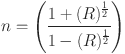 |
6 |
Figure 9a illustrates how the refractive index (n) of the deposited In2S3 thin films varies with wavelength. The study reveals that the refractive index increases with a higher silver doping mass quantity in the transparency region56. This indicates that improved thin-film crystallinity, associated with higher refractive index values, enhances the material’s suitability for optoelectronic applications. The following relationship (Eq. (7))57 describes the behavior of the extinction coefficient (k) in the fundamental absorption region.
 |
7 |
Fig. 9.

(a) The Variation of the refractive index (n) and (b) the extinction coefficient (k) versus wavelength of In2S3 (a) and Ag doped In2S3 thin films with various dopant levels (1% (b), 2% (c), 3% (d) and 4% (e)).
Figure 9b shows the extinction coefficient (k) plotted against wavelength for the samples. The data reveals a slight reduction in the extinction coefficient across the UV, visible, and near-IR regions with increasing silver doping. This decrease is attributed to the reduced light absorption at grain boundaries, which affects the overall absorption characteristics of the obtained films.
Conclusions
In2S3 and silver-doped In2S3 thin films were successfully deposited onto glass substrates using the vacuum thermal evaporation method. The study investigated the effects of doping on various physical properties, including crystal structure, surface morphology, optical characteristics, dielectric properties, bonding modes, and molecular structure. The doping of silver improved the crystallinity of the films; however, when the silver content exceeded 4%, the films nearly turn amorphous. Optical analysis demonstrated that the films achieved a transmission range of 50–90% in the near-infrared (IR) region, with the optical bandgap energy (Eg) decreasing from 2.23 eV to 2.03 eV as silver mass quantity increased. Additionally, the extinction coefficient and refractive index values were found to be dependent on the Ag doping levels. These findings suggest that Ag-doped In2S3 thin films are promising materials for solar energy applications due to their favorable optical properties and smooth surface morphology.
Acknowledgements
The authors extend their appreciation to Umm Al-Qura University, Saudi Arabia for funding this research work through grant number: 25UQU4320545GSSR07.
Author contributions
A. Timoumi: Conceptualization, Funding acquisition, Methodology, Project administration, Resources, Supervision, Writing – original draft, Writing – review and editing. S. N. Alamri: Formal analysis, Investigation, Methodology, Validation, Writing – original draft. Ziad Moussa: Formal analysis, Funding acquisition, Investigation, Methodology, Resources, Writing – original draft. Alaa S. Abd-El-Aziz: Formal analysis, Investigation, Resources, Writing – original draft Saleh A. Ahmed: Conceptualization, Formal analysis, Investigation, Methodology, Validation, Supervision, Funding acquisition, Project administration, Writing – original draft.
Funding
This research work was funded by Umm Al-Qura University, Saudi Arabia under grant number: 25UQU4320545GSSR07.
Data availability
This is to certify that all required and available data supported the work are included in the manuscript as figures and tables.
Declarations
Competing interests
The authors declare no competing interests.
Footnotes
Publisher’s note
Springer Nature remains neutral with regard to jurisdictional claims in published maps and institutional affiliations.
Contributor Information
A. Timoumi, Email: aotemoume@uqu.edu.sa
Alaa S. Abd-El-Aziz, Email: aabdelaziz@hrbeu.edu.cn
Saleh A. Ahmed, Email: saahmed@uqu.edu.sa
References
- 1.Mishra, S. R., Gadore, V. & Ahmaruzzaman, M. An overview of In2S3 and In2S3-based photocatalyst: characteristics, synthesis, modifications, design strategies, and catalytic environmental application. J. Environ. Chem. Eng.12(5), 113449 (2024). [Google Scholar]
- 2.Qiu, H., Fang, S., Huang, G. & Bi, J. A novel application of In2S3 for visible-light-driven photocatalytic inactivation of bacteria: Kinetics, stability, toxicity and mechanism. Environ. Res.190, 110018 (2020). [DOI] [PubMed] [Google Scholar]
- 3.Bazarchi, S. M., Esmaili, P. & Asgary, S. EPJ Appl. Phys.92, 10–1051 (2020). [Google Scholar]
- 4.Zhong, Z. Y., Cho, E. S. & Kwon, S. J. Effect of substrate temperatures on evaporated In2S3 thin film buffer layers for Cu (In, Ga) Se2 solar cells. Thin Solid Films547, 22–27 (2013). [Google Scholar]
- 5.Pulipaka, S., Koushik, A. K. S., Deepa, M. & Meduri, P. Enhanced photoelectrochemical activity of Co-doped β-In2S3 nanoflakes as photoanodes for water splitting. RSC Adv.9(3), 1335–1340 (2019). [DOI] [PMC free article] [PubMed] [Google Scholar]
- 6.Timoumi, A., Belhadj, W., Alamri, S. & Turkestani, M. A. Experimental studies and new theoretical modeling on the properties of In2S3 thin films. Opt. Mater.118, 111–238 (2021). [Google Scholar]
- 7.Kraini, M. et al. Properties of nickel doped In2S3 thin films deposited by spray pyrolysis technique. J. Mater. Sci. Mater. Electron.29, 1888–1906 (2018). [Google Scholar]
- 8.Saadallah, F., Jebbari, N., Kammoun, N. & Yacoubi, N. Optical and thermal properties of In2S3J. Colloid Interface Sci.491, 1–4 (2017).28011399 [Google Scholar]
- 9.Ranjith, R. et al. Post-deposition annealing effect on In2S3 thin films deposited using SILAR technique. Mater. Sci. Semiconduct. Process.10(1) 49–55 (2007). [Google Scholar]
- 10.Elfarrass, S., Hartiti, B., Ridah, A. & Tevenin, P. Effect of different S/In ratio of In2S3 films prepared by chemical spray pyrolysis method. J. Mater. Environ. Sci.6(2) 487 (2015). [Google Scholar]
- 11.Naghavi, N., Henriquez, R., Laptev, V. G. & Lincot, D. Growth studies and characterisation of In2S3 thin films deposited by atomic layer deposition (ALD). Appl. Surf. Sci., 222, 65–73 (2004). [Google Scholar]
- 12.Alsulamei, A. & Timoumi, A. Tailoring the physical and optical properties of Sn-doped In2S3 thin films obtained using VTE technique. Opt. Mater. X, 15, 100176 (2022). [Google Scholar]
- 13.Vallejo, W., Clavijo, J. & Gordillo, G. CGS based solar cells with In2S3 buffer layer deposited by CBD and coevaporation. Braz. J. Phys.40, 30–37 (2010). [Google Scholar]
- 14.Barreau, N., Bayon, R., Bernede, J. C. & Assmann, L. 203rd Meeting of the Elec trochemical Society, Paris, France, April 27–May 2, (2003).
- 15.Meng, X. et al. Fabrication and characterization of indium sulfide thin films deposited on SAMs modified substrates surfaces by chemical bath deposition. Appl. Surf. Sci.258, 649–656 (2011). [Google Scholar]
- 16.Gao, Z., Liu, J. & Wang, H. Investigation on growth of In2S3 thin films by chemical bath deposition. Mater. Sci. Semicond. Proc.15, 187–193 (2012).
- 17.Buecheler, S. et al. Ultrasonically sprayed indium sulfide buffer layers for Cu (In, Ga)(S, Se) 2 thin-film solar cells. Thin Solid Films, 517, 2312–2315 (2009). [Google Scholar]
- 18.Calixto-Rodriguez, M., Tiburcio-Silver, A., Ortiz, A. & Sanchez-Juarez, A. Optoelectronical properties of indium sulfide thin films prepared by spray pyrolysis for photovoltaic applications. Thin Solid Films, 480–481, 133–137 (2005). [Google Scholar]
- 19.Cherian, A. S., Mathew, M., Sudha Kartha, C. & Vijayakumar, K. P. Role of chlorine on the opto-electronic properties of β-In2S3 thin films. Thin Solid Films, 518, 1779–1783 (2010). [Google Scholar]
- 20.Otto, K., Katerski, A., Volobujeva, O., Mere, A. & Krunks, M. Indium sulfide thin films deposited by chemical spray of aqueous and alcoholic solutions. Energy Procedia, 3, 63–69 (2011). [Google Scholar]
- 21.Mostafa, N., Badawi, A. & Ahmed, S. Influence of Cu and Ag doping on structure and optical properties of In2O3 thin film prepared by spray pyrolysis. Results Phys.10, 126–131 (2018). [Google Scholar]
- 22.Alamoudi, E. & Timoumi, A. The synthesis and the effect of Cu on optoelectronic qualities of β-In2S3 as a window layer for CIGS thin film solar cells. Results Phys.40, 105858 (2022). [Google Scholar]
- 23.Atacan, K., Güy, N., Ozmen, M. & Ozacar, M. Fabrication of silver doped different metal oxide nanoparticles and evaluation of their antibacterial and catalytic applications. Appl. Surf. Sci. Adv.6, 100156 (2021). [Google Scholar]
- 24.Lin, P. et al. Optical and electrical properties of Ag-doped In2S3 thin films prepared by thermal evaporation. Adv. Mater. Sci. Eng. Article ID370861, (2014).
- 25.Sankır, N. D., Aydın, E. & Sankır, M. Impedance spectroscopy and dielectric properties of silver incorporated indium sulfide thin films. Int. J. Electrochem. Sci., 9, 3864–3875 (2014). [Google Scholar]
- 26.Alhammadi, S. et al. Effect of silver doping on the properties and photocatalytic performance of In2S3 nanoparticles. J. Mol. Liq., 344, 117649 (2021). [Google Scholar]
- 27.Wang, Y. et al. Cu-doped In2S3 hierarchical structures for photocatalytic organic dye degradation under visible light irradiation. Mater. Lett., 349, 134843, (2023). [DOI] [PubMed] [Google Scholar]
- 28.Wang, C. et al. Fe doping in In2S3 hollow nanotubes for efficient photo-Fenton degradation of emerging organic pollutants. Sep. Purif. Technol., 345, 127405 (2024). [Google Scholar]
- 29.Tivanova, M. S. et al. Effect of heat treatment in sulfur on structural, optical and electrical properties of thermally evaporated In2S3 thin films. Sol. Energy222, 290–297 (2021). [Google Scholar]
- 30.Tiss, B. et al. Electrical behavior and photocatalytic activity of Ag-Doped In2S3 thin films. J. Electron. Mater.50, 3739–3747 (2021). [Google Scholar]
- 31.Tiss, B. et al. Electrical transport of sprayed In2S3:Ag thin films. Mater. Sci. Semiconduct. Process., 114, 105080 (2020). [Google Scholar]
- 32.Terlemezoglu, M. A study on the structural, morphological and optical properties of Cu2-xse thin films deposited by thermal evaporation. BSEU J. Sci., 8(2), 1057–1063 (2021). [Google Scholar]
- 33.Jrad, F., Ben Naceur, J., Ouertani, R. & Chtourou, R. Photo-electrochemical impedance spectroscopy analysis of hydrothermally synthesized β-In2S3 thin film photo-anodes. Phys. E Low-Dimens. Syst. Nanostruct., 114, 113585 (2019). [Google Scholar]
- 34.Williamson, G. B. & Smallman, R. C. Dislocation densities in some annealed and cold-worked metals from measurements on the X-ray debye-scherrer spectrum. Philos. Mag, 1, 34–46 (1956). [Google Scholar]
- 35.El-Nahass, M. M., Khalifa, B. A., Soliman, H. S. & Seyam, M. A. M. Crystal structure and optical absorption investigations on β-In2S3 thin films. Thin Solid Films, 515, 1796–1801 (2006). [Google Scholar]
- 36.Souissi, R. et al. Thickness effect on VOC sensing properties of sprayed In2S3 films. RSC Adv.10(32), 18841–18852 (2020). [DOI] [PMC free article] [PubMed] [Google Scholar]
- 37.Nehra, S. P., Chander, S. & Sharma, A. Effect of thermal annealing on physical properties of vacuum evaporated In2S3 buffer layer for eco-friendly photovoltaic applications. Mater. Sci. Semicond. Process.40, 26 (2015). [Google Scholar]
- 38.Pentyala, N., Guduru, R. K., Shnerpunas, E. M. & Mohanty, P. S. Synthesis of ultrafine single crystals and nanostructured coatings of indium oxide from solution precursor. Appl. Surf. Sci.257, 6850–6857 (2011). [Google Scholar]
- 39.Revathi, N., Prathap, P., Subbaih, Y. P. V. & Ramakrishna Reddy, K. T. Substrate temperature dependent physical properties of In2S3 films. J. Phys. D Appl. Phys.41, 155404 (2008). [Google Scholar]
- 40.Bouguila, N. et al. Substrate temperature effect on properties of sprayed In2S3 films. J. Mater. Sci. Mater. Electron.26, 7639–7648 (2015). [Google Scholar]
- 41.Revathi, N., Prathap, P., Miles, R. W. & Reddy, K. T. R. Annealing effect on the physical properties of evaporated In2S3 films. Sol Energy Mater. Sol Cells94, 1487 (2010). [Google Scholar]
- 42.Jothibas, M., Manoharan, C., Ramalingam, S., Dhanapandian, S. & Bououdina, M. Spectrochim Acta Part. Mol. Biomol. Spec-trosc122, 171–178 (2014). [DOI] [PubMed] [Google Scholar]
- 43.Hameed, T. A., Wassel, A. R. & El Radaf, I. Investigating the effect of thickness on the structural, morphological, optical and electrical properties of AgBiSe2 thin films. J. Alloy Compd.805, 1–11 (2019). [Google Scholar]
- 44.Mahjabin, S. et al. Investigation of morphological, optical, and dielectric properties of RF sputtered WOx thin films for optoelectronic applications. Nanomaterials, 12, 3467 (2022). [DOI] [PMC free article] [PubMed] [Google Scholar]
- 45.Timoumi, A. et al. Unique growth and study on the unprecedented effects of fe doping Cu2AlSnS4 material fabricated by single vacuum system. J. Inorg. Organomet. Polym.33, 3146–3156 (2023). [Google Scholar]
- 46.Timoumi, A. & Bouzouita, H. Thickness dependent physical properties of evaporated In2S3 films for photovoltaic application. Inter J. Renew. Energy Technol. Res.2, 188–195 (2013). [Google Scholar]
- 47.Timoumi, A. et al. The effects of annealing process on the characteristics of β-In2S3 powder in pellet form. Mater. Sci. Semicond. Process.148, 106–717 (2022). [Google Scholar]
- 48.Timoumi, A., Bouzouita, H. & Rezig, B. Synthesis and characterization of In2S3: Na thin films preparedby vacuum thermal evaporation technique for photovoltaic applications. Eur. Phys. J. - Appl. Phys.42(3), 187–191 (2008). [Google Scholar]
- 49.Mohameda, J. & Amalraj, L. Effect of precursor concentration on physical properties of nebulized spray deposited In2S3 thin films. J. Asian Ceram. Soc.4, 357–366 (2016). [Google Scholar]
- 50.Gnenna, E., Khemiri, N. & Kanzari, M. Silver doping induced modifications in the physical properties of indium sulfide powders and thin films. J. Alloys Compd., 1021, 179625 (2025). [Google Scholar]
- 51.Ganesh, V., AlAbdulaal, T. H. & Yahia, I. S. Photo sensing properties of yttrium doped In2S3 thin film fabricated by low prize nebulizer spray pyrolysis technique. Phys. B Condens. Matter, 661, 414895 (2023). [Google Scholar]
- 52.Wang Lu, L., Yanjie Wu, X. & Tian, Y. Zr-doped β-In2S3 ultrathin nanoflakes as photoanodes: enhanced visible-light-driven photoelectrochemical water splitting. ACS Sustain. Chem. Eng., 4(5), 2606-2614 (2016).
- 53.Sharma, A. et al. Hydrothermally synthesized Sr-doped In2S3 microspheres for efficient degradation of noxious RhB pollutants in visible light exposure. J. Ind. Eng. Chem., 145, 360–371 (2025). [Google Scholar]
- 54.Esmaili, P. & Asgary, S. Al3+ doped In2S3 thin films: Structural and optical characterization Russ. J. Inorg. Chem.66, 621–628 (2021). [Google Scholar]
- 55.Alagarasan, D. et al. Fabrication of Bi-doped In2S3 thin films for highly sensitive UV photodetector applications. Mohd Shkir J. Photochem. Photobiol. Chem., 454, 115697 (2024). [Google Scholar]
- 56.Lin, C. Y. W., Channei, D., Koshy, P., Nakaruk, A. & Sorrell, C. C. Effect of Fe doping on TiO2 films prepared by spin coating. Ceram. Int.38, 3943–3946 (2012). [Google Scholar]
- 57.Albaidani, K., Timoumi, A., Belhadj, W., Alamri, S. N. & Ahmed, S. A. Structural, electronic and optical characteristics of TiO2 and Cu-TiO2 thin films produced by sol-gel spin coating. Ceram. Int.49(22) Part B, 36265–36275 (2023).
Associated Data
This section collects any data citations, data availability statements, or supplementary materials included in this article.
Data Availability Statement
This is to certify that all required and available data supported the work are included in the manuscript as figures and tables.