

Abstract
As a wide-band gap semiconductor, the formation of conductive layers on diamond surfaces is crucial for overcoming its insulating properties. Laser-induced doping has been demonstrated to be effective in generating low-resistance conductive layers on diamond. However, the underlying mechanism remains poorly understood. This study employs a multiscale characterization approach, including TOF-SIMS, Raman spectroscopy, AFM, and variable-temperature Hall measurements, to propose a novel mechanism for diamond surface conductivity, highlighting the synergistic interaction between defects and impurities. At the microscopic level, vacancies and interstitial atoms form diffusion channels for phosphorus; at the macroscopic scale, defect-induced localized states reduce the carrier activation energy to 0.0192 eV, facilitating hole conduction. Experiments demonstrate that 248 nm laser irradiation, with its higher photon energy, induces a denser defect network, significantly increasing phosphorus doping depth and concentration, resulting in a resistivity as low as 1.1 × 10⁻³ Ω·cm. This study systematically investigates the influence of laser parameters on the performance of conductive layers on diamond surfaces and proposes a novel laser-induced conduction mechanism, providing a solid foundation for the doping and conduction theoretical framework of ultrawide band gap semiconductors.

1. Introduction
The rapid development of carbon-based electronics has propelled research into low-dimensional materials such as carbon nanotubes and graphene, advancing micro- and nanoelectronics. − At the same time, diamond, as a prototypical wide-band gap semiconductor, has garnered attention for its exceptional physical and electronic properties, including a band gap of 5.47 eV, , a breakdown field strength of 20 MV/cm, and a thermal conductivity of 22 W·cm–1·K–1, positioning it as an ideal candidate for high-power electronic devices. , However, the inherent insulating nature of intrinsic diamond severely limits its practical applications, necessitating the development of efficient conductive layers on its surface. −
Due to the high chemical inertness and strong carbon–carbon bonds of diamond, traditional doping techniques (such as ion implantation) are difficult to implement effectively. High-energy ions can damage the diamond lattice, while the high activation energy required to activate dopants and the self-healing effect of the lattice during annealing may lead to the expulsion of dopants, further reducing the doping efficiency. High-temperature annealing, although capable of repairing ion implantation damage, often induces graphitization and reduces carrier mobility. − Recent advances in laser-induced doping techniques, which offer high spatiotemporal resolution and nonequilibrium processing capabilities, present a promising solution for diamond doping. − For instance, F.N. Li et al. developed an all-carbon deep-ultraviolet photodetector with diamond/graphite structure by laser-induced; Narayan et al. , demonstrated the transformation of amorphous carbon into nano diamond structures through laser irradiation; similarly, Eslam Abubakr et al. − used liquid-phase laser doping to form low-resistance conductive layers on diamond surfaces. Laser-induced phosphorus doping has emerged as an effective method for creating n-type diamond, utilizing the transient melting-quenching process to overcome the thermodynamic solubility limit and achieve high impurity concentrations. ,−
In this study, we employed phosphorus-containing solutions as doping sources to induce nanoscale structural changes on the diamond surface, resulting in low-resistance conductive layers. However, Hall measurements indicated that the conductive layer primarily supports hole conduction, contrary to the expected n-type conduction from phosphorus doping. This observation suggests that traditional doping models are insufficient to explain the conductivity mechanism of the laser-induced conductive layers. Thus, through a combination of laser-induced doping experiments, TOF-SIMS, Raman spectroscopy, AFM, and variable-temperature Hall testing, we propose a synergistic defect-impurity interaction mechanism for laser-induced conductivity on diamond surfaces. This theory systematically elucidates the conductive mechanism, where defect networks formed at the microscopic scale serve as high-efficiency diffusion channels for phosphorus, while defect-induced localized states at the macroscopic scale reduce the activation energy, ensuring low resistivity across a wide temperature range.
2. Experimental Section
Laser-Induced Doping Process
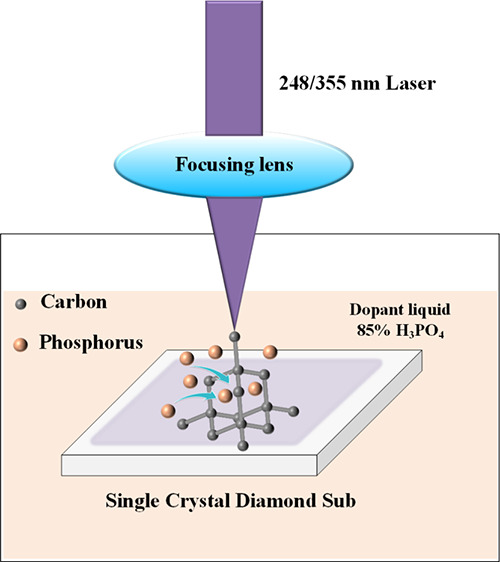
The diamond samples used were intrinsic IIa-type ⟨100⟩ single-crystal diamonds grown via Microwave plasma chemical vapor deposition (MPCVD), with dimensions of 10 × 10 × 0.5 mm. The gases used in the growth process of diamond samples are 300 sccm H2, 20 sccm CH4, and 1 sccm O2, without N2. The surface resistivity exceeded 109 Ω·cm (beyond the detection limit of the Hall effect measurement system). The diamond samples were immersed in an 85% phosphoric acid solution, with the liquid level positioned 2 cm above the sample surface. Subsequently, ultraviolet pulsed laser irradiation was applied to the diamond surface under normal temperature and pressure, with the substrate field size of 2 mm × 2 mm. The laser parameters during the experiment are detailed in the Table .
1. Different Laser Parameters.
| wavelengths (nm) | energy density (J/cm2) | frequencies (Hz) | number of irradiations (times) |
|---|---|---|---|
| 248 | 9.6 | 5 | 50 |
| 8.3 | 2 | 100 | |
| 6.9 | 150 | ||
| 200 | |||
| 355 | 13.1 | 10 | 50 |
| 6.9 | 5 | 100 | |
| 3.6 | 2 | 150 | |
| 200 | |||
According to experimental measurements, the loss rate of ultraviolet laser in this experiment is less than 5%, so the laser power is used as the experimental parameter. High-energy ultraviolet pulsed laser (Coherent Corp. Excimer laser; pulse duration 50 ns) irradiation induced a phase transition and melting on the diamond surface, forming a high-density defect network and capturing phosphorus impurities from the phosphoric acid solution, thereby resulting in a low-resistance conductive layer. The schematic diagram of the experimental setup is shown in Figure .
1.

Laser-induced doping experimental schematic.
Sample Processing and Characterization
Following laser treatment, the diamond samples were cleaned by immersion in a 50:50 nitric acid and sulfuric acid mixture at 250 °C for 60 min to remove graphite and amorphous carbon phases generated during growth or laser treatment. The samples were then sequentially ultrasonically cleaned in acetone, ethanol, and deionized water for 15 min each, followed by nitrogen blow-drying.
The samples were observed using a Leica DM2700 M microscope. Surface morphology was measured with a Bruker USA Dimension Icon Atomic Force Microscope (AFM), and surface roughness was calculated. Raman spectra were acquired using a HORIBA LabRAM HR Evolution Confocal Raman Microscope (wavelength: 532 nm; laser power: 10 mW; resolution: 0.5 cm–1). Electrical contacts were deposited using a DENTON EXPLORER-14 multisource electron beam evaporation system for subsequent electrical characterization. The resistivity and carrier concentration of the samples were measured using an Ecopia HMS-7000 Hall effect measurement system. Impurity element concentrations and their three-dimensional distribution within the sample were semiquantitatively analyzed with an ToF.SIMS 5–100 instrument (IONTOF GmbH; with 30 keV ions of Bi3 + High mass resolution mode and 1 keV ions of Cs+ Deep analysis mode; probe area 50 μm × 50 μm).
3. Results and Discussion
The changes of the surface morphology of the samples before and after laser treatment were observed by a microscope. The diamond surface without laser treatment (Figure a) is transparent and smooth, retaining only mechanical polishing marks. In contrast, the surface after laser irradiation (Figure c and Figure e) appears opaque brown. Acid washing and ultrasonic treatment with organic solvents fail to remove this region, suggesting that the defect-doping composite structure has been stably embedded into the crystal lattice. These images clearly highlight the changes in the surface morphology of the diamond before and after laser treatment, emphasizing the impact of laser-induced modifications. Therefore, we suppose that such variation is attributed not merely to the incorporation of impurities, but also to the lattice defects induced by the laser.
2.

(a, b) Microscope photos and AFM images of diamond surfaces before laser irradiation. (c, d) Microscope photos and AFM images of diamond surfaces after laser irradiation (355 nm, 6.9 J/cm2, 2 Hz, and 100 times). (e, f) microscope photos and AFM images of diamond surfaces after laser irradiation (248 nm, 6.9 J/cm2, 2 Hz, and 100 times).
The surface changes induced by laser irradiation were further characterized using atomic force microscopy (AFM), as depicted in Figure b, Figure d and Figure f. The surface roughness (Ra) in the laser-irradiated region increases from 0.671 to 1.589 nm. We believe that this morphological change reflects not only lattice disruption but also the nucleation and expansion of defects. The high-energy pulsed laser induces a transient melting-quenching process that causes vacancies and interstitial atoms to cluster, forming a high-density defect network. These defects act as fast diffusion channels for phosphorus atoms, enhancing doping efficiency, while the localized states they create establish paths for carrier transport.
In order to further analyze the crystal lattice changes of diamond and eliminate the influence of graphitization, the samples were characterized by Raman spectroscopy, and the results are shown in Figure . The work presented by Ali, M. A et al. shows Raman spectroscopy is 1 order of magnitude more sensitive to sp2 carbon than sp3 carbon due to the effective excitation of π states by visible photons. The sample retains the diamond characteristic peak at 1332.45 cm–1 after laser treatment, without any detectable G or D lines, indicating that no graphitization occurred or that any graphite was completely removed by acid washing. − These results imply that all observed changes are intrinsic to the sample itself. However, the full width at half-maximum (fwhm) of the peak increases from 3.48 cm–1 to 6.68 cm–1 and the intensity also decreased by 60%, indicating significant lattice distortion. ,,− This indicates that laser irradiation forms high-density defects, and phosphorus atoms are doped into the defects, causing local stress. The synergistic effect of defects and impurities reduces long-range lattice order, while the formation of short-range localized states promotes carrier hopping conduction, providing the structural basis for the observed changes in electrical properties.
3.

Raman spectrum of the diamond.
In order to determine the distribution of elemental phosphorus in diamond structure after laser induction, time-of-flight secondary ion mass spectrometry (TOF-SIMS) was used. Figure a indicates that phosphorus is uniformly distributed in the laser-irradiated region. Figure b shows phosphorus enrichment near the surface of the diamond, which correlates closely with the brown region observed in optical microscopy and the increase in AFM surface roughness. This suggests that the defect network significantly lowers the diffusion barrier, enhancing the incorporation of phosphorus. Figure c displays the distribution of phosphorus at varying depths under different laser wavelengths and energy densities. From the phosphorus detection intensity, we can semiquantitatively compare the phosphorus content under different laser conditions. The data shows that as the laser energy density increases, both the doping depth and concentration of phosphorus increase, further confirming that defect density and impurity concentration increase in tandem, reinforcing the role of the defect-impurity synergy in modifying the surface properties of diamond. At the same time, the 248 nm laser has higher photon energy, which can more efficiently induce transient melting of the diamond surface and promote the diffusion of phosphorus along the defect channels.
4.

(a) Two-dimensional distribution of phosphorus on the diamond surface by SIMS. (b) Three-dimensional distribution of phosphorus in the diamond by SIMS. (c) SIMS depth profile of phosphorus in the diamond.
Additionally, Hall test was used to characterize the resistivity of the conductive layer on the diamond surface under different laser conditions, as shown in Figure . As the number of irradiations increases, the defect density on the diamond surface increases, leading to greater phosphorus doping and further lattice distortion, thereby reducing the resistivity of the conductive layer. Additionally, under the same energy density, reducing the irradiation frequency increases the energy per laser pulse, significantly raising the defect density and further increasing phosphorus doping, thus lowering the resistivity. Notably, samples irradiated with 248 nm ultraviolet pulsed lasers show significantly lower resistivity compared to those irradiated with 355 nm lasers, reaching a minimum value of 1.1 × 10⁻³ Ω·cm. This suggests that higher photon energy forms a more extensive defect network, facilitating faster impurity diffusion and contributing more significantly to the defect-impurity synergy in the conductive layer.
5.

Changes in electrical resistivity under different irradiation times, frequencies, and wavelengths by Hall.
In order to further explore the conductive mechanism of diamond samples, Hall temperature variation was used to measure the temperature dependence of carrier concentration. Figure illustrates that carrier concentration increases linearly with temperature, and the slope is basically unchanged in the whole temperature range. The activation energies calculated by linear fits of the Arrhenius equation are 0.0192 and 0.0233 eV, respectively, which are significantly lower than the activation energy of the doped impurities. This suggests that the defect-assisted hopping conduction mechanism dominates across the entire temperature range (300–573 K). Notably, the carrier concentration change rate for the 248 nm laser-irradiated sample is significantly lower than that for the 355 nm laser sample, with a 21% reduction in temperature dependence. This phenomenon is attributed to the higher defect density induced by the higher energy laser, which increases the incorporation of impurities and enhances the conductivity of the conductive layer.
6.
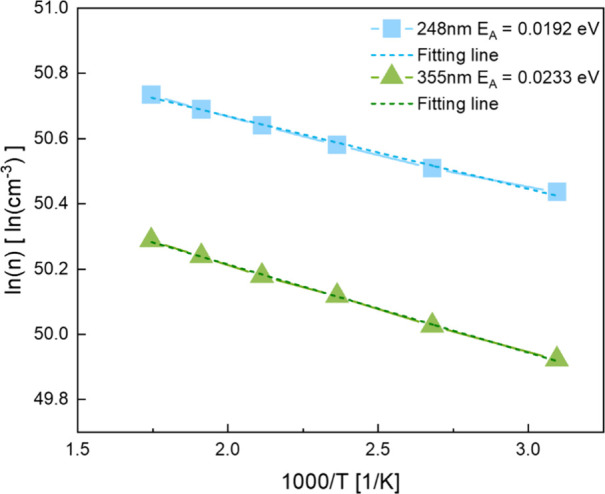
Temperature dependence of carrier concentration by Hall (same laser parameters: 6.9 J/cm2, 2 Hz, and 100 times).
Based on the multiscale characterization results from this study, we propose a defect-impurity synergistic mechanism for laser-induced conductivity on diamond surfaces, as shown in Figure . When the laser photon energy exceeds the band gap of diamond, such as with 193 nm laser irradiation, , electron–hole pairs are generated through direct interband transitions, inducing nonthermal lattice distortion that leads to local bond breaking and the formation of vacancy-interstitial atom pairs. For 248 and 355 nm lasers, the photon energy is below the band gap, and the primary mechanism involves multiphoton absorption and electron–phonon coupling, − inducing transient melting and forming a nanosecond-scale ultrafast melting layer. , Within the melting layer, carbon atoms rearrange, producing a high-density defect network. At the surface, high-energy pulsed lasers generate transient compressive stress, promoting the migration of vacancies toward the subsurface and providing rapid diffusion channels for impurities. During the melting stage, P5+ ions from the phosphoric acid solution are electrostatically adsorbed onto defect sites. The defect network lowers the diffusion barrier for phosphorus, significantly increasing its incorporation. In the quenching stage, the defect structure cools rapidly, with phosphorus atoms filling vacancies or bonding with interstitial atoms, preventing defect recombination and stabilizing the conductive channels, thus forming a stable defect-phosphorus composite. The main defect forms continuous tail states in the conduction band, and holes are transported via tunneling between the tail states or through nearest-neighbor hopping, resulting in an activation energy as low as 0.0192 eV. Furthermore, the density of tail states is extremely high, and carrier mobility is dominated by the hopping distance rather than thermal excitation, making the resistivity insensitive to temperature variations. This mechanism links laser energy, defect density, and doping levels, revealing the mechanism of nonequilibrium control for diamond surface conductive layers.
7.

Schematic diagram of the conductive mechanism.
4. Conclusions
This study presents a novel mechanism for the laser-induced defect-impurity synergistic conductive layer on diamond surfaces. The mechanism is validated through a range of characterization techniques, including optical microscopy, Raman spectroscopy, atomic force microscopy (AFM), time-of-flight secondary ion mass spectrometry (TOF-SIMS), and Hall effect measurements. The mechanism explains the experimental observations of low resistivity, low activation energy, high doping depth, high doping concentration, and high hole concentration, and highlights the dependence on laser parameters. Furthermore, it not merely reveals the mechanism of the laser-induced conductive layer on the surface of diamond, but also provides a new direction and theoretical basis for the controllable fabrication of the conductive layer of ultrawide band gap semiconductor.
Acknowledgments
L.G. and L.M. thank X. Zhang from Compound Semiconductor (Xiamen) Technology Co., Ltd. for AFM.
This work is supported by the National Key R&D Program of China (grant no. 2023YFB2807001), the Self-Deployed Project of the Shanghai Advanced Research Institute, Chinese Academy of Sciences (grant no. E2520F1ZZ1), the Project of the Shanghai Municipal Commission of Economy and Informatization (grant no. 2223107) and the Shanghai Special Project for Promoting High Quality Industrial Development (grant no. 2021008).
The authors declare no competing financial interest.
References
- May P. W.. The New Diamond Age? SCIENCE. 2008;319(5869):1490–1491. doi: 10.1126/science.1154949. [DOI] [PubMed] [Google Scholar]
- Wort C. J. H., Balmer R. S.. Diamond as an Electronic Material. Mater. Today. 2008;11(1–2):22–28. doi: 10.1016/S1369-7021(07)70349-8. [DOI] [Google Scholar]
- Aharonovich I., Neu E.. Diamond Nanophotonics. Advanced Optical Materials. 2014;2(10):911–928. doi: 10.1002/adom.201400189. [DOI] [Google Scholar]
- Guo L., Tian L., Wang H., Meng L., Feng C.. (Invited) Preparation of N-Type and P-Type Doped Single Crystal Diamonds with Laser-Induced Doping and Microwave Plasma Chemical Vapor Deposition. ECS Trans. 2024;113(7):23–36. doi: 10.1149/11307.0023ecst. [DOI] [Google Scholar]
- Watanabe H., Nebel C. E., Shikata S.. Isotopic Homojunction Band Engineering from Diamond. Science. 2009;324(5933):1425–1428. doi: 10.1126/science.1172419. [DOI] [PubMed] [Google Scholar]
- Tsao J. Y., Chowdhury S., Hollis M. A., Jena D., Johnson N. M., Jones K. A., Kaplar R. J., Rajan S., Van De Walle C. G., Bellotti E., Chua C. L., Collazo R., Coltrin M. E., Cooper J. A., Evans K. R., Graham S., Grotjohn T. A., Heller E. R., Higashiwaki M., Islam M. S., Juodawlkis P. W., Khan M. A., Koehler A. D., Leach J. H., Mishra U. K., Nemanich R. J., Pilawa-Podgurski R. C. N., Shealy J. B., Sitar Z., Tadjer M. J., Witulski A. F., Wraback M., Simmons J. A.. Ultrawide-Bandgap Semiconductors: Research Opportunities and Challenges. Adv. Elect Materials. 2018;4(1):1600501. doi: 10.1002/aelm.201600501. [DOI] [Google Scholar]
- Piracha A. H., Rath P., Ganesan K., Kühn S., Pernice W. H. P., Prawer S.. Scalable Fabrication of Integrated Nanophotonic Circuits on Arrays of Thin Single Crystal Diamond Membrane Windows. Nano Lett. 2016;16(5):3341–3347. doi: 10.1021/acs.nanolett.6b00974. [DOI] [PubMed] [Google Scholar]
- Rath P., Khasminskaya S., Nebel C., Wild C., Pernice W. H. P.. Diamond-Integrated Optomechanical Circuits. Nat. Commun. 2013;4(1):1690. doi: 10.1038/ncomms2710. [DOI] [PubMed] [Google Scholar]
- Zhu T., Li J.. Ultra-Strength Materials. Prog. Mater. Sci. 2010;55(7):710–757. doi: 10.1016/j.pmatsci.2010.04.001. [DOI] [Google Scholar]
- Li J., Shan Z., Ma E.. Elastic Strain Engineering for Unprecedented Materials Properties. MRS Bull. 2014;39(2):108–114. doi: 10.1557/mrs.2014.3. [DOI] [Google Scholar]
- Meng Y., Feng J., Han S., Xu Z., Mao W., Zhang T., Kim J. S., Roh I., Zhao Y., Kim D.-H., Yang Y., Lee J.-W., Yang L., Qiu C.-W., Bae S.-H.. Photonic van Der Waals Integration from 2D Materials to 3D Nanomembranes. Nat. Rev. Mater. 2023;8(8):498–517. doi: 10.1038/s41578-023-00558-w. [DOI] [Google Scholar]
- Montblanch A. R.-P., Barbone M., Aharonovich I., Atatüre M., Ferrari A. C.. Layered Materials as a Platform for Quantum Technologies. Nat. Nanotechnol. 2023;18(6):555–571. doi: 10.1038/s41565-023-01354-x. [DOI] [PubMed] [Google Scholar]
- Wu S., Guo K., Zhu J., Bai J., Wang Q.. Laser Assisted Solid Doping Promotes the Formation of Conductive Layer on the Surface of Single-Crystal Diamond. Surf. Coat. Technol. 2025;498:131846. doi: 10.1016/j.surfcoat.2025.131846. [DOI] [Google Scholar]
- Itsh’ak A., Klonsky O., Gelbstein Y., Beker P.. Doping Type Influence on Physical Diamond Properties. Mater. Res. Express. 2022;9(2):025901. doi: 10.1088/2053-1591/ac4eb8. [DOI] [Google Scholar]
- Koizumi S., Suzuki M.. n-Type Doping of Diamond. Physica Status Solidi (a) 2006;203(13):3358–3366. doi: 10.1002/pssa.200671407. [DOI] [Google Scholar]
- Liu Y., Li G., Gao N., Li H.. N-Type Doping of Diamond Surface by Potassium. Diamond Relat. Mater. 2023;140:110465. doi: 10.1016/j.diamond.2023.110465. [DOI] [Google Scholar]
- Bentini G. G., Bianconi M., Summonte C.. Surface Doping of Semiconductors by Pulsed-Laser Irradiation in Reactive Atmosphere. Appl. Phys. A: Mater. Sci. Process. 1988;45(4):317–324. doi: 10.1007/BF00617938. [DOI] [Google Scholar]
- Lee M., Ryu H.-Y., Ko E., Ko D.-H.. Effects of Phosphorus Doping and Postgrowth Laser Annealing on the Structural, Electrical, and Chemical Properties of Phosphorus-Doped Silicon Films. ACS Appl. Electron. Mater. 2019;1(3):288–301. doi: 10.1021/acsaelm.8b00057. [DOI] [Google Scholar]
- Narayan J., Bhaumik A., Haque A.. Pseudo-Topotactic Growth of Diamond Nanofibers. Acta Mater. 2019;178:179–185. doi: 10.1016/j.actamat.2019.08.008. [DOI] [Google Scholar]
- Zkria A., Abubakr E., Egiza M., Haque A., Narayan J., Yoshitake T.. Structural Evolution of Laser-Irradiated Ultrananocrystalline Diamond/Amorphous Carbon Composite Films Prepared by Coaxial Arc Plasma. Appl. Phys. Express. 2020;13(10):105503. doi: 10.35848/1882-0786/abb871. [DOI] [Google Scholar]
- Trusovas R., Račiukaitis G., Niaura G., Barkauskas J., Valušis G., Pauliukaite R.. Recent Advances in Laser Utilization in the Chemical Modification of Graphene Oxide and Its Applications. Advanced Optical Materials. 2016;4(1):37–65. doi: 10.1002/adom.201500469. [DOI] [Google Scholar]
- Stock F., Antoni F., Diebold L., Chowde Gowda C., Hajjar-Garreau S., Aubel D., Boubiche N., Le Normand F., Muller D.. UV Laser Annealing of Diamond-Like Carbon Layers Obtained by Pulsed Laser Deposition for Optical and Photovoltaic Applications. Appl. Surf. Sci. 2019;464:562–566. doi: 10.1016/j.apsusc.2018.09.085. [DOI] [Google Scholar]
- Sartori A. F., Orlando S., Bellucci A., Trucchi D. M., Abrahami S., Boehme T., Hantschel T., Vandervorst W., Buijnsters J. G.. Laser-Induced Periodic Surface Structures (LIPSS) on Heavily Boron-Doped Diamond for Electrode Applications. ACS Appl. Mater. Interfaces. 2018;10(49):43236–43251. doi: 10.1021/acsami.8b15951. [DOI] [PMC free article] [PubMed] [Google Scholar]
- Li F. N., Bao H. W., Li Y., Ma F., Wang H. X.. Laser Induced Diamond/Graphite Structure for All-Carbon Deep-Ultraviolet Photodetector. Appl. Surf. Sci. 2023;636:157818. doi: 10.1016/j.apsusc.2023.157818. [DOI] [Google Scholar]
- Narayan J., Bhaumik A., Sachan R., Haque A., Gupta S., Pant P.. Direct Conversion of Carbon Nanofibers and Nanotubes into Diamond Nanofibers and the Subsequent Growth of Large-Sized Diamonds. Nanoscale. 2019;11(5):2238–2248. doi: 10.1039/C8NR08823C. [DOI] [PubMed] [Google Scholar]
- Narayan J., Bhaumik A., Gupta S., Haque A., Sachan R.. Progress in Q-Carbon and Related Materials with Extraordinary Properties. Materials Research Letters. 2018;6(7):353–364. doi: 10.1080/21663831.2018.1458753. [DOI] [Google Scholar]
- Abubakr E., Zkria A., Katamune Y., Ohmagari S., Imokawa K., Ikenoue H., Yoshitake T.. Formation of Low Resistivity Layers on Singlecrystalline Diamond by Excimer Laser Irradiation. Diamond Relat. Mater. 2019;95:166–173. doi: 10.1016/j.diamond.2019.04.013. [DOI] [Google Scholar]
- Abubakr E., Ohmagari S., Zkria A., Ikenoue H., Pernot J., Yoshitake T.. Formation of P-n+ Diamond Homojunctions by Shallow Doping of Phosphorus through Liquid Emersion Excimer Laser Irradiation. Materials Research Letters. 2022;10(10):666–674. doi: 10.1080/21663831.2022.2083457. [DOI] [Google Scholar]
- Abubakr E., Ohmagari S., Zkria A., Ikenoue H., Yoshitake T.. Laser-Induced Novel Ohmic Contact Formation for Effective Charge Collection in Diamond Detectors. Materials Science in Semiconductor Processing. 2022;139:106370. doi: 10.1016/j.mssp.2021.106370. [DOI] [Google Scholar]
- Abubakr E., Zkria A., Ohmagari S., Katamune Y., Ikenoue H., Yoshitake T.. Laser-Induced Phosphorus-Doped Conductive Layer Formation on Single-Crystal Diamond Surfaces. ACS Appl. Mater. Interfaces. 2020;12(51):57619–57626. doi: 10.1021/acsami.0c18435. [DOI] [PubMed] [Google Scholar]
- Bhaumik A., Sachan R., Gupta S., Narayan J.. Discovery of High-Temperature Superconductivity (T c = 55 K) in B-Doped Q-Carbon. ACS Nano. 2017;11(12):11915–11922. doi: 10.1021/acsnano.7b06888. [DOI] [PubMed] [Google Scholar]
- Haque A., Sachan R., Narayan J.. Synthesis of Diamond Nanostructures from Carbon Nanotube and Formation of Diamond-CNT Hybrid Structures. Carbon. 2019;150:388–395. doi: 10.1016/j.carbon.2019.05.027. [DOI] [Google Scholar]
- Ikeda A., Marui D., Ikenoue H., Asano T.. Nitrogen Doping of 4H-SiC by KrF Excimer Laser Irradiation in Liquid Nitrogen. Jpn. J. Appl. Phys. 2015;54(4S):04DP02. doi: 10.7567/JJAP.54.04DP02. [DOI] [Google Scholar]
- Salter P. S., Booth M. J., Courvoisier A., Moran D. A. J., MacLaren D. A.. High Resolution Structural Characterisation of Laser-Induced Defect Clusters inside Diamond. Appl. Phys. Lett. 2017;111(8):081103. doi: 10.1063/1.4993118. [DOI] [Google Scholar]
- Zhu H., Qin J., Long W., Song X., Jing P.. Research Status of Crack Problem in Laser Brazing Diamond. J. Iron Steel Res. Int. 2024;31(10):2329–2343. doi: 10.1007/s42243-024-01322-2. [DOI] [Google Scholar]
- M. Ali A., Deckert-Gaudig T., Egiza M., Deckert V., Yoshitake T.. Near- and Far-Field Raman Spectroscopic Studies of Nanodiamond Composite Films Deposited by Coaxial Arc Plasma. Appl. Phys. Lett. 2020;116(4):041601. doi: 10.1063/1.5142198. [DOI] [Google Scholar]
- Palyanov Y. N., Kupriyanov I. N., Sokol A. G., Khokhryakov A. F., Borzdov Y. M.. Diamond Growth from a Phosphorus-Carbon System at High Pressure High Temperature Conditions. Cryst. Growth Des. 2011;11(6):2599–2605. doi: 10.1021/cg2003468. [DOI] [Google Scholar]
- Ager J. W., Veirs D. K., Rosenblatt G. M.. Spatially Resolved Raman Studies of Diamond Films Grown by Chemical Vapor Deposition. Phys. Rev. B. 1991;43(8):6491–6499. doi: 10.1103/PhysRevB.43.6491. [DOI] [PubMed] [Google Scholar]
- Srimongkon K., Ohmagari S., Kato Y., Amornkitbamrung V., Shikata S.. Boron Inhomogeneity of HPHT-Grown Single-Crystal Diamond Substrates: Confocal Micro-Raman Mapping Investigations. Diamond Relat. Mater. 2016;63:21–25. doi: 10.1016/j.diamond.2015.09.014. [DOI] [Google Scholar]
- Shakhov F. M., Abyzov A. M., Kidalov S. V., Krasilin A. A., Lähderanta E., Lebedev V. T., Shamshur D. V., Takai K.. Boron-Doped Diamond Synthesized at High-Pressure and High-Temperature with Metal Catalyst. J. Phys. Chem. Solids. 2017;103:224–237. doi: 10.1016/j.jpcs.2016.11.020. [DOI] [Google Scholar]
- Haque A., Pant P., Narayan J.. Large-Area Diamond Thin Film on Q-Carbon Coated Crystalline Sapphire by HFCVD. J. Cryst. Growth. 2018;504:17–25. doi: 10.1016/j.jcrysgro.2018.09.036. [DOI] [Google Scholar]
- Ohmagari S., Yamada H., Umezawa H., Tsubouchi N., Chayahara A., Mokuno Y.. Growth and Characterization of Freestanding P+ Diamond (100) Substrates Prepared by Hot-Filament Chemical Vapor Deposition. Diamond Relat. Mater. 2018;81:33–37. doi: 10.1016/j.diamond.2017.11.003. [DOI] [Google Scholar]
- Bogdan G., Nesládek M., D’Haen J., Haenen K., D’Olieslaeger M.. Freestanding (100) Homoepitaxial CVD Diamond. Diamond Relat. Mater. 2006;15(4–8):508–512. doi: 10.1016/j.diamond.2005.10.059. [DOI] [Google Scholar]
- Angeloni L. A., Baryshev S. V., Mühle M., Schroeder W. A.. Spectral Emission Properties of a Nitrogen-Doped Diamond (001) Photocathode: Hot Electron Transport and Transverse Momentum Filtering. Phys. Rev. B. 2023;107(16):165105. doi: 10.1103/PhysRevB.107.165105. [DOI] [Google Scholar]
- Jia G., Wang K., Zhang Y., Guo R., Xiao Z., Wu Y., Tian Y.. Photoluminescence Spectra of Intrinsic Interstitials in IIa Diamond after near Threshold Energy Irradiation. Vacuum. 2021;187:110107. doi: 10.1016/j.vacuum.2021.110107. [DOI] [Google Scholar]
- Guo Z., Wang L., Wang K., Ren C., Guo R., Zhang Y., Tian Y., Wang H.. Temperature Dependent Thermal Conductivity of IIa Diamond by Laser Excited Raman Spectroscopy. Appl. Phys. Lett. 2021;118(19):192104. doi: 10.1063/5.0046656. [DOI] [Google Scholar]
- Kononenko V. V.. Modification of Diamond Surface by Femtosecond Laser Pulses. Photonics. 2023;10(10):1077. doi: 10.3390/photonics10101077. [DOI] [Google Scholar]
- Gao Y.-C., Zhao J.-H., Wang X.-P., Chen N.-K.. First-Principles Research on Mechanism of Sub-Band Absorption of Amorphous Silicon Induced by Ultrafast Laser Irradiation. Results in Physics. 2021;31:104941. doi: 10.1016/j.rinp.2021.104941. [DOI] [Google Scholar]
- Chen N., Wang R., Nagarajan B., Yan B., Wu Y., He N., Castagne S.. Investigation of Metal-Coating-Assisted IR Nanosecond Pulsed Laser Ablation of CVD Diamond. Journal of Materials Research and Technology. 2022;18:4114–4129. doi: 10.1016/j.jmrt.2022.04.072. [DOI] [Google Scholar]
- Uchida K., Suzuki Y., Watanabe K.. Thermal Effects on Laser-Assisted Field Evaporation from a Si Surface: A Real-Time First-Principles Study. J. Appl. Phys. 2019;126(3):034302. doi: 10.1063/1.5090949. [DOI] [Google Scholar]
- Kononenko V. V., Vlasov I. I., Gololobov V. M., Kononenko T. V., Semenov T. A., Khomich A. A., Shershulin V. A., Krivobok V. S., Konov V. I.. Nitrogen-Vacancy Defects in Diamond Produced by Femtosecond Laser Nanoablation Technique. Appl. Phys. Lett. 2017;111(8):081101. doi: 10.1063/1.4993751. [DOI] [Google Scholar]
- Dong X., Wang Y., Song X.. Physical Mechanisms for the Optical Properties of the Femtosecond-Laser-Treated Black Diamond. J. Phys.: Condens. Matter. 2020;32(16):165502. doi: 10.1088/1361-648X/ab6740. [DOI] [PubMed] [Google Scholar]
- Polyakov V. I., Rukovishnikov A. I., Garin B. M., Avdeeva L. A., Heidinger R., Parshin V. V., Ralchenko V. G.. Electrically Active Defects, Conductivity, and Millimeter Wave Dielectric Loss in CVD Diamonds. Diamond Relat. Mater. 2005;14(3–7):604–607. doi: 10.1016/j.diamond.2004.10.001. [DOI] [Google Scholar]