

Abstract
Template-stripped substrates provide on-demand access to clean, ultraflat gold surfaces, avoiding the need for laborious cleaning procedures or the use of expensive single-crystal electrodes. While these gold/adhesion layer/support sandwich structures are most conveniently prepared through the application of epoxy or optical adhesives, such composites exhibit instabilities in organic solvents that limit their wider application. Here we demonstrate that substrates with solvent-impermeable metal films can be used in previously problematic chemical environments after integration into a protective, custom-built (electrochemical) flow cell. We apply our methodology to probe different self-assembled monolayers, observing reproducible alkanethiol reductive desorption features, an exemplary redox response using 6-(ferrocenyl)hexanethiol, and corroborate findings that cobalt(II) bis(terpyridine) assemblies exhibit a low coverage. This work significantly extends the utility of these substrates, relative to mechanically polished or freshly deposited alternatives, particularly for studies of systems involving adsorbed molecules whose properties are strongly influenced by the nanoscopic features of the metal-solution interface.
Keywords: template-stripping, gold thin films, self-assembled monolayers, electrochemistry, three-dimensional printing

Gold surfaces are extensively utilized in studies spanning molecular self-assembly, , electrocatalysis, , biosensing, and molecular electronics , due to their electrical conductivity, resistance to oxidation, and straightforward chemical functionalization. In many applications it is important that these surfaces are flat at atomic length scales (ideally with a single crystallographic orientation) and free from contamination. This enables the resolution of nanoscale surface features in scanning probe microscopy (SPM) experiments, , and helps improve measurement reproducibility. Pristine surfaces can be produced directly using techniques such as the Clavilier method (involving careful polishing and thermal annealing), evaporation of gold onto freshly cleaved mica held at 300 °C (facilitating epitaxial growth), or chemical mechanical polishing. While the quality of gold surfaces decreases rapidly upon exposure to air (through the adsorption of water and adventitious contaminants), , they may be reconditioned through exposure to “piranha” solution, mechanical or electrochemical polishing, or UV-ozone/plasma cleaning. However, such formation and cleaning methods are often expensive and/or time-intensive, particularly when substrates must be freshly prepared before every experiment, and sometimes require specialized equipment.
In stark contrast, the use of “template-stripped” substrates ,, provides convenient, on-demand, access to clean, ultraflat gold surfaces (AuTS). Here, a gold thin film is first evaporated onto a well-defined template such as silicon , or mica. , Next, ∼ 1 cm2 pieces of silicon or glass support are attached to the “as-deposited” metal surface using an epoxy , or optical adhesive. As needed, individual gold/adhesion layer/support sandwich structures are then chemically (through immersion in an appropriate solvent, alkanethiol solution) or mechanically (by flexing the template, using a blade) cleaved from the substrate. , The gold surface that was previously in contact with the template, and so protected from the ambient atmosphere, is then immediately utilized. SPM imaging studies have demonstrated these surfaces, which can exhibit a root-mean-squared roughness of <0.5 nm over micrometer length scales, are flatter than as-deposited , or even single-crystal substrates. This general methodology has been extended to prepare high-quality thin films of other metals including silver, , platinum, , palladium, and nickel. , The early developments and principal applications of template-stripped substrates were reviewed in 2012 by Vogel et al.
Despite clear advantages, a major practical limitation to the use of such substrates results from the poor solvent resistance of the adhesive (Figure a). Swelling of this polymeric material, or even delamination, can significantly damage the metal film. With NOA 61, a commonly utilized optical adhesive, this occurs after relatively short exposure to dichloromethane (CH2Cl2, 10 min), acetone, acetonitrile (MeCN, 5 h), or tetrahydrofuran (THF, 1 d; see the Supporting Information, NOA 61 Adhesive-Solvent Screening). As a result, many molecules of interest cannot easily be exposed to these near-perfect surfaces to form self-assembled monolayers (SAMs), given their poor solubility in adhesive-compatible solvents (e.g., H2O, EtOH). Interfacial chemical reactions and analytical experiments (including solution/surface voltammetry) may not be performed in preferred media. While these challenges have been addressed through several creative strategies over the past 30 years, which focus on improving or replacing the adhesive to improve the solvent resistance of the substrate (described in the Supporting Information, Alternative Strategies to Form Solvent-Resistant TS Substrates), no single approach has yet been advanced that completely resolves this problem.
1.

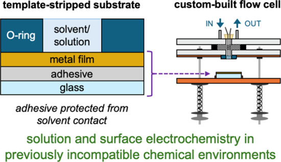
(a) Straightforward access to ultraflat and clean gold surfaces is provided using template-stripped gold (AuTS) substrates, which are cleaved immediately prior to use from a silicon wafer support. However, the adhesives commonly applied in the preparation of these substrates are incompatible with several solvents. (b) We propose the solvent-incompatibility of these substrates can be circumvented by restricting solvent/solution exposure to the top surface of the thin metal film using a chemically resistant O-ring. (c) A schematic of the electrochemical flow cell developed here for use with template-stripped substrates (open configuration). This comprises the following major elements: (i) septum with inserted electrodes; (ii) electrochemical flow cell top; (iii) cell compartment base; (iv) substrate holder; (v) spring compression mechanism. Additional features of the cell are labeled in Figure S2. (d) A photo of a first-generation electrochemical flow cell (closed configuration).
In contrast to these methods, here we show that AuTS surfaces may be used in any (gold-compatible) chemical environment by protecting the supporting adhesive to maintain its integrity. By limiting solvent exposure to a well-defined area of the metal thin film, the film itself, along with a chemically resistant O-ring, serves as a robust barrier that safeguards the substrate from damage (Figure b). This strategy enables the extended use of adhesive-incompatible solvents with template-stripped substrates for the first time. Specifically, we show that template-stripped gold/copper bilayer substrates (Au/CuTS) uniquely exhibit solvent-impermeable metal films which facilitate their use in previously problematic chemical environments after integration into a protective, custom-built (electrochemical) flow cell (Figure c,d). We demonstrate these Au/CuTS can be used as (modified) working electrodes for electrochemical measurements in CH2Cl2 solutions, and apply them here to characterize SAMs formed in situ from CH2Cl2 or MeCN solutions. While AuTS have been extensively used for surface electrochemical studies, and to form SAMs, we stress that such investigations have typically only exposed the substrate to adhesive-compatible solvents. The proof-of-concept experiments presented here highlight the wider range of experiments that can be conducted using our distinct approach, while further underscoring the utility of applying these contaminant-free, structurally consistent electrode surfaces to evaluate the properties of adsorbed molecular assemblies. Unless stated, all metal thin films used here were prepared through thermal evaporation onto silicon wafer templates, and NOA 61 was used to attach ∼ 1 cm2 glass supports to the as-deposited surface (Figure a, full details provided in the Supporting Information). When relevant, we note the thickness of each film in nanometers using subscripts (for example, Au200/Cu600 TS indicates 200 nm of gold and 600 nm of copper).
2.

(a) Schematic showing the composition of template-stripped substrates prepared with a single gold film (AuTS) or a gold/copper bilayer film (Au/CuTS). (b) Images of backlit substrates (cropped to show an area of ∼ 1 cm2) comprising films with visible defects (left; bright white regions) and without apparent defects (right). We indicate the thickness of each metal film in nanometers using subscripts; for example, Au200 TS describes a substrate with a 200 nm layer of gold. (c) Representative images of backlit substrates (cropped to show an area of ∼ 1 cm2) after 1 h exposure to CH2Cl2 to the top of the film (solvent restricted to a well-defined area using an O-ring). When solvent can interact with the adhesive through defects in the film, we observe the formation of blisters (left) or near complete film delamination (right; the example provided here corresponds to a substrate that was intentionally damaged by forming a single hole with a sharp needle). Diffuse features in the images are reflections of the microscope used to take these photos.
We first evaluated the stability of different AuTS and Au/CuTS thin films toward contact with CH2Cl2, a notoriously problematic solvent. Here, each substrate was inspected with a backlit microscope, both immediately after cleavage, then again after 1 h of continuous, O-ring localized, solvent exposure to a well-defined surface area. As illustrated in Figure b for Au200 TS, this imaging technique allows us to identity visible imperfections in the freshly cleaved film. We suggest defects form where the metal-adhesive layer is weaker/thinner (proximal to residual air bubbles), and/or result from the poor structural integrity of the metal film itself, which allow portions of the film to remain on the template after the substrate is cleaved. This observation is consistent with an early report that Au200 TS prepared with epoxy did not survive exposure to solvents such as THF or CDCl3/MeOH using an O-ring-connected reaction chamber due to small and infrequent discontinuities in the gold film. Accordingly, we prepared and tested AuTS with greater film thicknesses (≤2000 nm), reasoning that the deposition of additional material would ultimately yield robust and complete substrates after template-stripping. Certainly, as the film thickness increased, fewer obvious defects were observed. However, after 1 h of CH2Cl2 exposure, all AuTS tested exhibited signs of damage – from blister formation to complete film loss (illustrative examples are shown in Figure c). While it has been proposed that a thickness of 600 nm should be sufficient to ensure there are no cracks or pinholes in the gold film, our results indicate that solvents such as CH2Cl2 can in fact penetrate films up to 2000 nm thick. We note, in attempting to reconcile the origin of these persistent defects, that there is a large difference in the coefficients of linear expansion for gold and silicon (α = 14.2 and 2.6 × 10⁻⁶ K–1 at ∼ 25 °C, respectively). This mismatch could lead to the film shrinking relative to the template as it cools after deposition, separating individual crystal grains and facilitating solvent interactions with the adhesive.
To identify a deposition protocol that provides solvent-impermeable metal surfaces, we set out to deposit bilayer films comprising copper deposited onto gold. Here, copper was chosen primarily to avoid the use of substantial quantities of gold, which is more expensive. Surprisingly, our initial analyses of Au200/Cu200–1000 TS showed they often yielded cleaved metal films with fewer visible defects than pure gold films of the same total thickness (Figure b). After careful placement of O-rings to avoid any visible imperfections, these films typically also survived exposure to CH2Cl2 without apparent damage. Additional studies are needed to establish the exact origin of this improved solvent resistance; however, we suggest this may result from postdeposition growth of native copper oxide on the as-deposited surface which serves to bridge any open channels in the film. While this approach to form robust gold substrates can be further improved, for example, to mitigate the possibility of surface contamination with copper (see the SI for additional discussion), these model Au/CuTS could be immediately applied across a series of proof-of-concept experiments.
We subsequently developed a low cost, custom-built (electrochemical) flow cell that can be used with any template-stripped substrate, illustrated in Figure c,d. Full details of the construction and use of this apparatus is described in the Supporting Information. Briefly, the cell is built using commercially available and/or three-dimensionally (3D) printed parts. Substrates are interfaced with an O-ring using a guided, spring-loaded platform to minimize damage to the exposed surface, then secured by tightening the thumb nuts and/or clamping in place. The O-ring engaged with the substrate forms the bottom of a cell compartment of approximate volume ∼ 1 cm2. The system can be fitted with different flow cell tops for experiments involving aqueous or organic media, which are introduced and removed using a peristaltic pump that transfers liquid or gas through the compartment via the in/out ports. Critically, our cell design ensures only a well-defined area of the template-stripped surface is exposed to the solvent/solution environment. By introducing counter and reference electrodes via a septa cap positioned in the cell top, we can exploit electrically contacted template-stripped metal surfaces as working electrodes in electrochemical experiments. Substrate loading in the flow cell takes <5 min, faster or comparable to the time typically required to clean a mechanically polished substrate (AuMP). The integrity of each substrate is verified after every experiment.
We first demonstrate the capabilities of our substrates and flow cell by performing solution electrochemical studies of ferrocene in 0.1 M nBu4N-PF6/CH2Cl2 using an Au200/Cu400 TS working electrode. Critically, this medium is incompatible with such substrates utilized through conventional methods (Figure S13b). Our cell design can accommodate O-rings with three distinct inner diameters (IDs): 0.120” (small), 0.150” (medium), and 0.195” (large). In Figure a, we plot overlaid cyclic voltammograms obtained using these different O-rings that clearly show that the intensity of the reversible ferrocene Fe2+/3+ redox wave increases with the size of the exposed working area (see Figure S5 for voltammograms obtained at different scan rates, V s). We plot, in Figure b, the theoretical area calculated using the ID against the measured area (determined using the Randles–Ševčík equation) for each O-ring size (data provided in Table S3), which yields an excellent linear correlation. Notably, the measured areas are consistently ∼ 90% of the theoretical value, which we attribute to O-ring compression and/or solvent swelling during use. Importantly, we find no significant change in working electrode area or visible signs of damage, even after extended exposure to CH2Cl2 electrolyte solution (5–17 h, Figure S6). Together, these results firmly illustrate the improved stability of optical adhesive-based template-stripped substrates employed with this approach (otherwise compromised in <10 min), and the efficacy of our cell design to perform electrochemical experiments. Cells equipped with the large O-rings are used in all subsequent experiments, unless stated.
3.

Solution electrochemical data. (a) Overlaid solution cyclic voltammograms for a 0.1 mM solution of ferrocene (FcH, structure inset) in 0.1 M nBu4N-PF6/CH2Cl2 (scan rate (V s) = 0.1 V/s) obtained using Au200/Cu400 TS as working electrodes, with small (pink), medium (teal), and large (blue) substrate O-rings. Voltammograms at different V s are provided in Figure S5. (b) A plot of the theoretical working electrode surface area (determined using the inner diameter of the O-ring) against the measured area (obtained through application of the Randles–Ševčík equation, using i pa for cyclic voltammograms of FcH measured at V s = 1 V/s) reveals an excellent linear correlation. (c) Overlaid cyclic voltammograms obtained using AuTS and mechanically polished gold (AuMP) electrodes in 0.01 M H2SO4/H2O using a conventional large volume electrochemical cell (V s = 0.05 V/s). The current of the AuMP electrode is multiplied by a factor of ∼15 to normalize the intensity of the gold reduction features observed at ∼0.8 V.
These template-stripped surfaces were subjected to further characterization using aqueous electrochemistry. In Figure c we plot representative cyclic voltammograms obtained using AuTS and AuMP working electrodes in 0.01 M H2SO4/H2O using a conventional large volume electrochemical cell (data from repeated experiments is provided in Figure S7). We find that voltammograms obtained using AuTS exhibit comparable gold oxidation features (observed at potentials >1 V) with a principal component at ∼1.24 V (vs Ag/AgCl) that we attribute to oxidation of Au(111) crystal facets. Crystallites with this orientation are expected to dominate the AuTS surface. ,,, In contrast, voltammograms obtained using AuMP show noticeable variation in the oxidation features from experiment to experiment, as is expected given the rougher, polycrystalline surfaces of these electrodes generated through mechanical polishing by hand. Notably, voltammograms obtained for AuTS under the same conditions, but now using our low volume flow cell, provided oxidation features that changed in form and intensity with repeated potential cycling (Figure S8). This voltammetric response has previously been associated with the presence of Cl– ions in solution that have leaked from the Ag/AgCl (3 M KCl) reference electrode. While this issue may be circumvented by using a different reference electrode, we emphasize that our flow cell can already be utilized for other aqueous electrochemical experiments, as further evidenced below.
We next apply template-stripped substrates, integrated into our electrochemical flow cell, to study different SAMs formed using the molecular components shown in Figure a. It is reiterated at this point that clean, atomically flat substrates with a single-dominant crystallographic orientation are ideal electrodes for such (electrochemical) investigations. This is well demonstrated, for example, in studies of large-area molecular junctions, where the surface topology significantly influences the variability of conductivity measurements. , Broadly, it is considered that atomically flat surfaces help facilitate the formation of crystalline 2D molecular assemblies that closely pack with fewer defects, in which the variations in molecule–surface contact geometries, and the nanoscale chemical environment around individual components, are minimized. ,,
4.

Surface electrochemical data. (a) Structures of the molecules used to form self-assembled monolayers (SAMs). (b) Overlaid voltammograms for SAMs of CnSH (n = 6, 8, 10) on an AuTS working electrode (prepared ex situ), measured in 0.1 M KOH/H2O (V s = 0.05 V/s). Each voltammogram shows a dominant peak feature attributed to the reductive desorption of the SAM. (c) A plot of n against the desorption peak potential (average of 6 measurements) exhibits a linear correlation (dashed line fit, slope = −24 mV/n), in agreement with previous reports. , Error bars correspond to one standard deviation. (d) A cyclic voltammogram for a SAM of FcSH on a Au200/Cu400 TS working electrode, prepared in situ using a 0.1 mM CH2Cl2 solution, and measured in 0.1 M nBu4N-PF6/CH2Cl2 (V s = 0.1 V/s). (e) A cyclic voltammogram for a SAM of CoSS on a Au200/Cu200 TS working electrode, prepared in situ using a 1 mM MeCN solution, and measured in 0.1 M nBu4N-PF6/CH2Cl2 (V s = 1 V/s).
In Figure b, we present overlaid linear sweep voltammograms for AuTS electrodes modified with 1-hexanethiol (C6SH), 1-octanethiol (C8SH), and 1-decanethiol (C10SH) SAMs formed ex situ, measured in 0.1 M KOH/H2O (a representative cyclic voltammogram is provided in Figure S9). In each case, we observe a dominant, sharp peak feature upon the first cathodic sweep that we assign to reductive desorption of the monolayer. Consistent with previous studies, the peak potential for this redox event shifts to more negative values as the length of the alkane chain increases, reflecting the improved thermodynamic stability of longer chain alkanethiol SAMs. , The well-defined nature of each peak provides additional evidence that these monolayers are well-organized. Disordered SAMs, or SAMs formed on polycrystalline surfaces, are found to exhibit significantly broadened desorption peaks, or multiple features of significant intensity. , We further plot, in Figure c, the number of carbons in each alkane (n) against the average reductive desorption potential for each SAM (obtained from measurements of six modified electrodes). The excellent linear correlation (dashed line) highlights the highly reproducible properties of CnSH SAMs formed on AuTS.
In Figure d and e, we plot voltammograms measured in 0.1 M nBu4N-PF6/CH2Cl2 using Au/CuTS electrodes that have been functionalized with SAMs formed in situ from 6-(ferrocenyl)hexanethiol (FcSH) or [Co(tpySS)2](PF6)2 (CoSS, where tpySS = 4′-(methyldisulfide)-2,2′:6′,2″terpyridine), respectively. To form the SAM, the cell compartment was fitted with a freshly cleaved substrate then charged with a FcSH/CH2Cl2 or CoSS/MeCN solution. After 1 h, pure solvent was flowed through the system to wash away any unbound species, followed by electrolyte solution. For each modified electrode we observe an electrochemical response characteristic of a single, surface-immobilized reversible redox-active species (i pa/i pc ∼ 1, i p ∝ V s; Figure S10a, Figure S11, Table S4). , We emphasize again here that such experiments cannot easily be performed with template-stripped substrates using conventional approaches due to the incompatibility of the adhesive with CH2Cl2 (Figure S13b). The preparation and study of CoSS SAMs at such high-quality electrode surfaces using any other method would have required the use of single-crystal electrodes, as this compound exhibits relatively poor solubility in AuTS-compatible solvents such as EtOH or H2O.
We attribute the redox feature of the FcSH SAM to the Fe2+/3+ event of adsorbed ferrocenyl groups. The redox peak separation (E p) < 10 mV at slow scan rates (Figure S10b), and full width at half maximum (E fwhm) of 77 mV (at V s = 0.1 V/s), observed for this SAM approach the theoretical values for noninteracting redox sites. , Using the measured electrode area (Table S3) we calculate a surface coverage (Γ) of 224 pmol/cm2. This is ∼73% of the value reported for a saturation coverage (Γsat.) SAM formed on an AuTS substrate. We attribute the near ideal redox response of our FcSH SAM to Γ < Γsat., which reduces unfavorable intermolecular steric interactions in the adsorbed layer; the atomic flatness of the underlying substrate which minimizes monolayer inhomogeneities; and the organic electrolytic microenvironment that homogenizes the redox-response through better interfacial solvation of the adsorbed components. − The voltammetric response presented in Figure d contrasts sharply with the broad, multicomponent peak features typically observed in studies of analogous monolayers in aqueous electrochemical environments (even when using AuTS). ,,, This exemplary result clearly highlights the advantages of studying SAMs formed on clean, ultraflat gold surfaces in different (organic) solvent environments, experiments facilitated here using solvent-impermeable Au/CuTS substrates.
The redox waves observed for the CoSS SAM are assigned to the Co2+/3+ couple. We have previously observed these charged complexes yield SAMs on AuMP substrates with consistently low saturation surface coverages (∼40 pmol/cm2), as well as ΔE p and ΔEfwhm values indicative of significant lateral intercomponent repulsive interactions. , This was attributed to the loss of mobile PF6 – counterions from CoSS upon surface binding, such that the resulting adsorbed [Co(tpySS)2]2+ species may form only loosely packed 2D arrays which mitigate unfavorable lateral long-range Coulomb forces. We find, as indicated in Table S4, that CoSS SAMs formed here on pristine Au200/Cu200 TS surfaces exhibit highly comparable electrochemical properties to those formed on AuMP. Importantly, this reveals that the unusual adsorption behavior of CoSS, and analogous compounds with Fe2+, Zn2+, and Ru2+ centers, , is not attributable to the relatively large surface roughness or adventitious contamination of AuMP (e.g., following contact with alumina slurry or piranha solution), further motivating additional studies of these and other charged SAMs to evaluate the role of electrostatic interactions on their structure, composition, and stability.
In conclusion, we have shown how solvent-impermeable thin metal films, integrated within an (electrochemical) flow cell, can be exploited to utilize template-stripped substrates in otherwise challenging chemical environments. As demonstrated here using Au/CuTS, our approach significantly extends the range of possible experiments involving these near-ideal electrodes. Specifically, it facilitates the reproducible formation of well-ordered SAMs comprising a greater number of components (accommodating different solubilities), also providing a facile mechanism to characterize and modify them ,, in different media. More broadly, this work introduces a conceptually distinct process to obtain such solvent-resistant substrates, targeting procedures which provide continuous, defect-free films rather than improvements to the adhesive. In principle our strategy is compatible with substrates prepared using any template or adhesive, allowing these to be selected independently on their own merit (primarily targeting, for example, an adhesive’s temperature stability, or thermal/electrical conductivity, rather than its solvent resistance). We anticipate these methods may ultimately be extended to thin films of other materials, studies under an inert atmosphere or at different temperatures, and the use of flow cells as reaction vessels, further expanding the utility of template-stripped substrates in all areas of surface science.
Supplementary Material
Acknowledgments
This work was primarily supported by University of Southern California (USC) startup funds and the National Science Foundation (NSF CAREER Award to M.S.I., CHE-2239614). We thank Thomas M. Czyszczon-Burton for assistance with acquiring X-ray photoelectron spectroscopic data, and Temin Sohn for help with refining our approach to constructing the flow cell. M.S.I. thanks Latha Venkataraman for the use of her laboratory to perform the NOA 61 Adhesive-Solvent Screening study. Instrumentation in the USC Chemistry Instrument Facility was acquired with support from the USC Research and Innovation Instrumentation Award Program. Additionally, funds provided by the NSF (DBI-0821671, CHE-0840366) and National Institutes of Health (S10 RR25432) supported the acquisition of the NMR spectrometers used in our work.
The Supporting Information is available free of charge at https://pubs.acs.org/doi/10.1021/acsnanoscienceau.5c00018.
FlowCell info (ZIP)
FlowCell info (ZIP)
Additional experimental details and discussion, a guide to constructing and operating the flow cell, electrochemical and X-ray photoelectron spectroscopic data, a NOA 61 Adhesive-Solvent Screening study, .step and .stl files for 3D printable flow cell parts (PDF)
The authors declare no competing financial interest.
References
- Mali K. S., Pearce N., De Feyter S., Champness N. R.. Frontiers of Supramolecular Chemistry at Solid Surfaces. Chem. Soc. Rev. 2017;46(9):2520–2542. doi: 10.1039/C7CS00113D. [DOI] [PubMed] [Google Scholar]
- Love J. C., Estroff L. A., Kriebel J. K., Nuzzo R. G., Whitesides G. M.. Self-Assembled Monolayers of Thiolates on Metals as a Form of Nanotechnology. Chem. Rev. 2005;105(4):1103–1170. doi: 10.1021/cr0300789. [DOI] [PubMed] [Google Scholar]
- Sévery L., Szczerbiński J., Taskin M., Tuncay I., Brandalise Nunes F., Cignarella C., Tocci G., Blacque O., Osterwalder J., Zenobi R., Iannuzzi M., Tilley S. D.. Immobilization of Molecular Catalysts on Electrode Surfaces Using Host–Guest Interactions. Nature Chem. 2021;13(6):523–529. doi: 10.1038/s41557-021-00652-y. [DOI] [PubMed] [Google Scholar]
- Rodriguez P., Koper M. T. M.. Electrocatalysis on Gold. Phys. Chem. Chem. Phys. 2014;16(27):13583–13594. doi: 10.1039/C4CP00394B. [DOI] [PubMed] [Google Scholar]
- Wink T., Van Zuilen S. J., Bult A., Van Bennekom W. P.. Self-Assembled Monolayers for Biosensors. Analyst. 1997;122(4):43–50. doi: 10.1039/a606964i. [DOI] [PubMed] [Google Scholar]
- Su T. A., Neupane M., Steigerwald M. L., Venkataraman L., Nuckolls C.. Chemical Principles of Single-Molecule Electronics. Nature Rev. Mater. 2016;1(3):16002. doi: 10.1038/natrevmats.2016.2. [DOI] [Google Scholar]
- Vilan A., Aswal D., Cahen D.. Large-Area, Ensemble Molecular Electronics: Motivation and Challenges. Chem. Rev. 2017;117(5):4248–4286. doi: 10.1021/acs.chemrev.6b00595. [DOI] [PubMed] [Google Scholar]
- Hegner M., Wagner P., Semenza G.. Ultralarge Atomically Flat Template-Stripped Au Surfaces for Scanning Probe Microscopy. Surf. Sci. 1993;291(1–2):39–46. doi: 10.1016/0039-6028(93)91474-4. [DOI] [Google Scholar]
- Butt H.-J., Wang D. N., Hansma P. K., Kühlbrandt W.. Effect of Surface Roughness of Carbon Support Films on High-Resolution Electron Diffraction of Two-Dimensional Protein Crystals. Ultramicroscopy. 1991;36(4):307–318. doi: 10.1016/0304-3991(91)90123-N. [DOI] [Google Scholar]
- Clavilier J., Faure R., Guinet G., Durand R.. Preparation of Monocrystalline Pt Microelectrodes and Electrochemical Study of the Plane Surfaces Cut in the Direction of the {111} and {110} Planes. J. Electroanal. Chem. Interf. Electrochem. 1980;107(1):205–209. doi: 10.1016/S0022-0728(79)80022-4. [DOI] [Google Scholar]
- DeRose J. A., Thundat T., Nagahara L. A., Lindsay S. M.. Gold Grown Epitaxially on Mica: Conditions for Large Area Flat Faces. Surf. Sci. 1991;256(1–2):102–108. doi: 10.1016/0039-6028(91)91204-B. [DOI] [Google Scholar]
- Miller M. S., Ferrato M.-A., Niec A., Biesinger M. C., Carmichael T. B.. Ultrasmooth Gold Surfaces Prepared by Chemical Mechanical Polishing for Applications in Nanoscience. Langmuir. 2014;30(47):14171–14178. doi: 10.1021/la5032027. [DOI] [PubMed] [Google Scholar]
- Turetta N., Sedona F., Liscio A., Sambi M., Samorì P. Au. Surface Contamination in Ambient Conditions: Unravelling the Dynamics of the Work Function in Air. Adv. Mater. Interfaces. 2021;8(10):2100068. doi: 10.1002/admi.202100068. [DOI] [Google Scholar]
- Blackstock J. J., Li Z., Jung G.. Template Stripping Using Cold Welding. J. Vac. Sci. Technol. A. 2004;22(3):602. doi: 10.1116/1.1710492. [DOI] [Google Scholar]
- Pan W., Durning C. J., Turro N. J.. Kinetics of Alkanethiol Adsorption on Gold. Langmuir. 1996;12(18):4469–4473. doi: 10.1021/la9408634. [DOI] [Google Scholar]
- Carvalhal R. F., Sanches Freire R., Kubota L. T.. Polycrystalline Gold Electrodes: A Comparative Study of Pretreatment Procedures Used for Cleaning and Thiol Self-Assembly Monolayer Formation. Electroanalysis. 2005;17(14):1251–1259. doi: 10.1002/elan.200403224. [DOI] [Google Scholar]
- King D. E.. Oxidation of Gold by Ultraviolet Light and Ozone at 25 °C. J. Vac. Sci. Technol. A. 1995;13(3):1247–1253. doi: 10.1116/1.579869. [DOI] [Google Scholar]
- Dermody D. L., Lee Y., Kim T., Crooks R. M.. Synthesis, Characterization, and Chemical Sensitivity of Self-Assembled Bilayers Composed of Polydiacetylenes and Calix[4]Arenes Chemically Modified on the Upper Rim. Langmuir. 1999;15(24):8435–8440. doi: 10.1021/la981080b. [DOI] [Google Scholar]
- Vogel N., Zieleniecki J., Köper I.. As Flat as It Gets: Ultrasmooth Surfaces from Template-Stripping Procedures. Nanoscale. 2012;4(13):3820–3832. doi: 10.1039/c2nr30434a. [DOI] [PubMed] [Google Scholar]
- Weiss E. A., Kaufman G. K., Kriebel J. K., Li Z., Schalek R., Whitesides G. M.. Si/SiO2-Templated Formation of Ultraflat Metal Surfaces on Glass, Polymer, and Solder Supports: Their Use as Substrates for Self-Assembled Monolayers. Langmuir. 2007;23(19):9686–9694. doi: 10.1021/la701919r. [DOI] [PubMed] [Google Scholar]
- Stamou D., Gourdon D., Liley M., Burnham N. A., Kulik A., Vogel H., Duschl C.. Uniformly Flat Gold Surfaces: Imaging the Domain Structure of Organic Monolayers Using Scanning Force Microscopy. Langmuir. 1997;13(9):2425–2428. doi: 10.1021/la962123w. [DOI] [Google Scholar]
- Wagner P., Hegner M., Guentherodt H.-J., Semenza G.. Formation and in Situ Modification of Monolayers Chemisorbed on Ultraflat Template-Stripped Gold Surfaces. Langmuir. 1995;11(10):3867–3875. doi: 10.1021/la00010a043. [DOI] [Google Scholar]
- Ragan R., Ohlberg D., Blackstock J. J., Kim S., Williams R. S.. Atomic Surface Structure of UHV-Prepared Template-Stripped Platinum and Single-Crystal Platinum(111) J. Phys. Chem. B. 2004;108(52):20187–20192. doi: 10.1021/jp0466789. [DOI] [Google Scholar]
- Diebel J., Löwe H., Samorí P., Rabe J. P.. Fabrication of Large-Scale Ultra-Smooth Metal Surfaces by a Replica Technique. Appl. Phys. A. 2001;73(3):273–279. doi: 10.1007/s003390100935. [DOI] [Google Scholar]
- Blackstock J. J., Li Z., Freeman M. R., Stewart D. R.. Ultra-Flat Platinum Surfaces from Template-Stripping of Sputter Deposited Films. Surf. Sci. 2003;546(2–3):87–96. doi: 10.1016/j.susc.2003.09.039. [DOI] [Google Scholar]
- Senthil Kumar K., Jiang L., Nijhuis C. A.. Fabrication of Ultra-Smooth and Oxide-Free Molecule-Ferromagnetic Metal Interfaces for Applications in Molecular Electronics under Ordinary Laboratory Conditions. RSC Adv. 2017;7(24):14544–14551. doi: 10.1039/C6RA27280K. [DOI] [Google Scholar]
- Alessandrini A., Bortolotti C. A., Bertoni G., Vezzoli A., Facci P.. Ultraflat Nickel Substrates for Scanning Probe Microscopy of Polyhistidine-Tagged Proteins. J. Phys. Chem. C. 2008;112(10):3747–3750. doi: 10.1021/jp0771623. [DOI] [Google Scholar]
- Haynes, W. M. CRC Handbook of Chemistry and Physics; CRC Press, 2014. [Google Scholar]
- Bard, A. J. ; Faulkner, L. Y. . Electrochemical Methods; Wiley, 2004. [Google Scholar]
- Hamelin A.. Cyclic Voltammetry at Gold Single-Crystal Surfaces. Part 1. Behaviour at Low-Index Faces. J. Electroanal. Chem. 1996;407(1–2):1–11. doi: 10.1016/0022-0728(95)04499-X. [DOI] [Google Scholar]
- Lee S., Bae S.-S., Medeiros-Ribeiro G., Blackstock J. J., Kim S., Stewart D. R., Ragan R.. Scanning Tunneling Microscopy of Template-Stripped Au Surfaces and Highly Ordered Self-Assembled Monolayers. Langmuir. 2008;24(12):5984–5987. doi: 10.1021/la800265q. [DOI] [PubMed] [Google Scholar]
- Hugall J. T., Finnemore A. S., Baumberg J. J., Steiner U., Mahajan S.. Solvent-Resistant Ultraflat Gold Using Liquid Glass. Langmuir. 2012;28(2):1347–1350. doi: 10.1021/la204299h. [DOI] [PubMed] [Google Scholar]
- Xu X., Makaraviciute A., Pettersson J., Zhang S.-L., Nyholm L., Zhang Z.. Revisiting the Factors Influencing Gold Electrodes Prepared Using Cyclic Voltammetry. Sens. Actuators B: Chem. 2019;283:146–153. doi: 10.1016/j.snb.2018.12.008. [DOI] [Google Scholar]
- Yuan L., Jiang L., Zhang B., Nijhuis C. A.. Dependency of the Tunneling Decay Coefficient in Molecular Tunneling Junctions on the Topography of the Bottom Electrodes. Angew. Chem. Int. Ed. 2014;53(13):3377–3381. doi: 10.1002/anie.201309506. [DOI] [PubMed] [Google Scholar]
- Weiss E. A., Chiechi R. C., Kaufman G. K., Kriebel J. K., Li Z., Duati M., Rampi M. A., Whitesides G. M.. Influence of Defects on the Electrical Characteristics of Mercury-Drop Junctions: Self-Assembled Monolayers of n-Alkanethiolates on Rough and Smooth Silver. J. Am. Chem. Soc. 2007;129(14):4336–4349. doi: 10.1021/ja0677261. [DOI] [PubMed] [Google Scholar]
- Losic D., Shapter J. G., Gooding J. J.. Influence of Surface Topography on Alkanethiol SAMs Assembled from Solution and by Microcontact Printing. Langmuir. 2001;17(11):3307–3316. doi: 10.1021/la001462t. [DOI] [Google Scholar]
- Leopold M. C., Black J. A., Bowden E. F.. Influence of Gold Topography on Carboxylic Acid Terminated Self-Assembled Monolayers. Langmuir. 2002;18(4):978–980. doi: 10.1021/la011683e. [DOI] [Google Scholar]
- Shin-ichiro Imabayashi S., Minehiko Iida M., Daisuke Hobara D., Zhi Qiang Feng Z. Q., Katsumi Niki K., Takashi Kakiuchi T.. Reductive Desorption of Carboxylic-Acid-Terminated Alkanethiol Monolayers from Au(111) Surfaces. J. Electroanal. Chem. 1997;428(1–2):33–38. doi: 10.1016/S0022-0728(97)00006-5. [DOI] [Google Scholar]
- Widrig C. A., Chung C., Porter M. D.. The Electrochemical Desorption of N-Alkanethiol Monolayers from Polycrystalline Au and Ag Electrodes. J. Electroanal. Chem. Interf. Electrochem. 1991;310(1–2):335–359. doi: 10.1016/0022-0728(91)85271-P. [DOI] [Google Scholar]
- Walczak M. M., Alves C. A., Lamp B. D., Porter M. D.. Electrochemical and X-Ray Photoelectron Spectroscopic Evidence for Differences in the Binding Sites of Alkanethiolate Monolayers Chemisorbed at Gold. J. Electroanal. Chem. 1995;396(1):103–114. doi: 10.1016/0022-0728(95)04056-T. [DOI] [Google Scholar]
- Eckermann A. L., Feld D. J., Shaw J. A., Meade T. J.. Electrochemistry of Redox-Active Self-Assembled Monolayers. Coord. Chem. Rev. 2010;254(15):1769–1802. doi: 10.1016/j.ccr.2009.12.023. [DOI] [PMC free article] [PubMed] [Google Scholar]
- Nerngchamnong N., Thompson D., Cao L., Yuan L., Jiang L., Roemer M., Nijhuis C. A.. Nonideal Electrochemical Behavior of Ferrocenyl–Alkanethiolate SAMs Maps the Microenvironment of the Redox Unit. J. Phys. Chem. C. 2015;119(38):21978–21991. doi: 10.1021/acs.jpcc.5b05137. [DOI] [Google Scholar]
- Huffman B. L., Bredar A. R. C., Dempsey J. L.. Origins of Non-Ideal Behaviour in Voltammetric Analysis of Redox-Active Monolayers. Nature Rev. Chem. 2024;8(8):628–643. doi: 10.1038/s41570-024-00629-8. [DOI] [PubMed] [Google Scholar]
- Tian H., Qi L., Xiang D., Shao H., Yu H.-Z.. Homogenized Redox Behavior of Electroactive Self-Assembled Monolayers on Gold in the Organic Phase. Electrochim. Acta. 2015;170:369–375. doi: 10.1016/j.electacta.2015.04.143. [DOI] [Google Scholar]
- Creager S. E., Rowe G. K.. Redox Properties of Ferrocenylalkane Thiols Coadsorbed with Linear N-Alkanethiols on Polycrystalline Bulk Gold Electrodes. Anal. Chim. Acta. 1991;246(1):233–239. doi: 10.1016/S0003-2670(00)80680-7. [DOI] [Google Scholar]
- Chidsey C. E. D., Bertozzi C. R., Putvinski T. M., Mujsce A. M.. Coadsorption of Ferrocene-Terminated and Unsubstituted Alkanethiols on Gold: Electroactive Self-Assembled Monolayers. J. Am. Chem. Soc. 1990;112(11):4301–4306. doi: 10.1021/ja00167a028. [DOI] [Google Scholar]
- Trang C. D. M., Saal T., Inkpen M. S.. Methyldisulfide Groups Enable the Direct Connection of Air-Stable Metal Bis(Terpyridine) Complexes to Gold Surfaces. Dalton Trans. 2023;52:7836–7842. doi: 10.1039/D3DT00955F. [DOI] [PMC free article] [PubMed] [Google Scholar]
- Trang C. D. M., Mora Perez C., Ran J., Prezhdo O. V., Inkpen M. S.. Counterion Loss from Charged Surface-Bound Complexes Drives the Formation of Loosely Packed Monolayers. J. Am. Chem. Soc. 2024;146:25625–25639. doi: 10.1021/jacs.4c07327. [DOI] [PMC free article] [PubMed] [Google Scholar]
- Heo J., Ahn H., Won J., Son J. G., Shon H. K., Lee T. G., Han S. W., Baik M.-H.. Electro-Inductive Effect: Electrodes as Functional Groups with Tunable Electronic Properties. Science. 2020;370:214–219. doi: 10.1126/science.abb6375. [DOI] [PubMed] [Google Scholar]
- Chechik V., Crooks R. M., Stirling C. J. M.. Reactions and Reactivity in Self-Assembled Monolayers. Adv. Mater. 2000;12(16):1161–1171. doi: 10.1002/1521-4095(200008)12:16<1161::AID-ADMA1161>3.0.CO;2-C. [DOI] [Google Scholar]
Associated Data
This section collects any data citations, data availability statements, or supplementary materials included in this article.