

Abstract
The demand for rapid, field‐deployable detection of hazardous substances has intensified the search for plasmonic sensors with both high sensitivity and fabrication simplicity. Conventional approaches to plasmonic substrates, however, often rely on lithographic precision or complex chemistries limiting scalability and reproducibility. Here, a facile, one‐step synthesis of vertically aligned 2D nanosheets composed of intergrown Cu2O/CuO crystallites is presented, fabricated via oxygen plasma discharge on copper substrates. Decorated with a discontinuous Ag nanoparticle layer, the substrates serve as high‐performance plasmonic metasurface exhibiting nanomolar sensitivity of explosive molecules, with detection limits as low as 4–5 nm for tetryl and 2–3 nm for HMX under 488 nm excitation. Importantly, the SERS (Surface enhanced Raman scattering) activity expands into a broad spectral range (488, 535, 633 nm), enabled by the formation of plasmonic “hotspots” network within nanoparticle gaps, crevices, that cumulatively boost SERS signal. A pronounced red‐shift in the symmetric NO2 stretching mode of tetryl is further demonstrated, attributed to LUMO‐mediated charge transfer from the Ag Fermi level—highlighting the need for laser‐ and substrate‐sensitive interpretation of vibrational data. Together, these findings advance the rational design of low‐cost, reproducible SERS substrates for trace chemical detection, with potential for integration into autonomous sensing platforms.
Keywords: explosives, metamaterials, plasma synthesis, plasmonic metasurfaces, SERS
One‐step oxygen plasma sculpting of copper into vertically aligned oxide nanosheets is reported via energetic ion bombardment and defect‐mediated growth. Magnetron‐sputtered silver nanoparticles decorate these sheets to yield a plasmonic metasurface whose network of hot spots amplifies multi‐wavelength SERS signals for explosive and related hazardous‐chemical detection at nanomolar levels with high analytical precision.

1. Introduction
Surface‐enhanced Raman spectroscopy (SERS) is a leading technique for fingerprinting molecular structural dynamics at ultralow concentrations, enabled by localised surface plasmon resonances that amplify Raman scattering signals near the surface of metallic nanostructures by several orders of magnitude.[ 1 , 2 ] Its potential in real‐world sensing, ranging from environmental monitoring to forensic explosives detection, critically depends on the quality of the underlying plasmonic substrate.[ 3 , 4 ] Among various nanostructured platforms, vertically aligned 2D architectures offer unmatched near‐field confinement and high surface accessibility, making them ideal candidates for reproducible, high‐sensitivity SERS.[ 5 , 6 ] However, scalable fabrication of such vertically oriented 2D metasurfaces remains a persistent challenge.
A wide range of synthesis techniques, including laser‐assisted patterning, thermal oxidation, and chemical vapor deposition, solution‑based chemical and electrochemical growth, template‑assisted and glancing‐angle deposition, and nature‑inspired or green methods, have been employed to produce vertically aligned nanostructures from metal oxides, carbon‑based architectures (e.g., CNTs, graphene), and hybrid composites with further decoration using nanoparticles by drop‐casting or sputtering of Au, Ag films for SERS purposes.[ 7 , 8 ] Still conventional approaches bring some imitations associated either with high cost, complex processing steps, and poor adaptability to field deployment.[ 9 , 10 , 11 ] Wet‐chemical or thermal oxidation strategies can produce metal oxide nanostructures, but rarely yield the vertical morphologies required for optimal SERS enhancement.[ 12 ] These technological factors underscore the need for simpler, more versatile fabrication strategies that can generate the desired vertical geometries while retaining material and structural heterogeneity ‐ an essential feature for broadband plasmonic activity. Plasma‐based processes, on the other hand, have proven to be very promising for the production of high‐quality functional nanostructures made of transition metals, carbonaceous materials, and polymers[ 13 , 14 , 15 ] They offer the possibility of tailoring the desired morphology with atomic precision in a single step.[ 16 , 17 ] This can advance fabrication strategies for SERS‐active patterns and metasurfaces, overcoming the decades‐lasting limitations of classical bottom‐up and top‐bottom approaches.[ 18 ]
In this work, we present a one‐step plasma oxidation method to engineer vertically aligned CuO/Cu2O nanosheets directly on copper substrates. Rather than pursuing perfect uniformity, our method harnesses plasma‐induced stresses, rapid oxidation kinetics, and energetic ion bombardment to drive the coalescence of 1D oxide growth fronts into extended 2D sheet‐like domains.[ 19 , 20 ] These intergrown CuO/Cu2O nanosheets exhibit wedge‐like geometries and stacking faults that increase structural complexity and surface roughness. Upon Ag nanoparticle decoration, the resulting metasurface displays highly localized electromagnetic fields, supported by both simulation and experimental analysis, which span a wide excitation range (488–633 nm). These homogenously distributed plasmonic “hotspots” at the surface of 2D sheets, which are formed at crevices, edges, and nanoparticle junctions, and are crucial for achieving reproducible and tunable SERS enhancement.[ 21 , 22 , 23 ]
Importantly, we show that this platform enables the detection of explosive molecules (HMX and tetryl) at nanomolar levels, with clear vibrational signatures that shift depending on excitation wavelength. The most informative Raman mode corresponding to the symmetric stretching vibrations of the N═O bond in tetryl can be located at very different positions, namely at 1328, 1335, and 1376 cm−1 for 488, 535, and 633 nm lasers, respectively. This spectral tunability is attributed to LUMO‐mediated charge transfer between the analyte and silver nanoparticles, resulting in redshifts and broadening of the NO2 stretching bands; a key mechanistic insight with implications for SERS data standardization and spectral database development. Together, our findings demonstrate that structural imperfections and disorder, which are often viewed as a drawback, can be strategically employed to create versatile, high‐performance metasurfaces for molecular sensing at trace concentrations. This opens a pathway toward cost‐effective, lithography‐free SERS metasurface platforms with potential for portable detection systems in security, environmental, and biomedical applications.
2. Experimental Section
2.1. Plasma Setup and Synthesis Process
A schematic representation of the experimental setup and the arrangement of the samples on the cathode surface can be found in (Figure 1a). The setup was installed in a cylindrical stainless steel vacuum chamber with a diameter of 300 mm and a length of 350 mm. Both the cathode and the anode were made of graphite and had a cylindrical shape with the dimensions ∅40 mm × 6 mm (cathode) and ∅15 mm × 5 mm (anode). The distance between the electrodes was 30 mm. A disk‐shaped copper screen with a diameter of 100 mm and a thickness of 1 mm was placed under the cathode, which was put under a floating electrical potential. A graphite insert with a diameter of 8 mm and a height of 6 mm was installed in the center of the cathode. At a distance of 4.5 mm, two copper samples with a diameter of 8 mm and a height of 5 mm were placed on the cathode so that their flat surfaces (front surfaces) were facing the graphite sample. The scheme was used to ensure a high discharge current and the necessary level of heating to the copper samples.
Figure 1.

a) Plasma setup used for oxidation of copper samples; b) Averaged Raman spectrum from the spots indicated by yellow squares; c) XRD patterns showing a coexistence of Cu2O (red) and CuO (blue) phases.
Before inserting into the vacuum chamber, the samples were cleaned in an ultrasonic bath with isopropyl alcohol. After ion cleaning of the samples in argon plasma, oxygen was supplied to the chamber until the pressure reached the value of 350 Pa. After the ignition of a conventional glow discharge, an operation mode with the discharge voltage of 630 V and the discharge current of 0.25 A was reached (P = 155–160 W, the reflected power was kept below 5 W), while the operation was interrupted by short arcs developed over the surface of the graphite insert every 2–5 s. The arc ignition resulted in changing the geometry of the insert from cylindrical to the shape of a truncated cone due to erosion. Thus, the graphite insert served as a mean to change the stable mode of glow discharge operation to the glow‐to‐arc transition mode, which was supposed to change the conditions for the synthesis of copper oxide nanostructures developed on the surface of copper samples. During the experiment, the temperature of the copper samples was measured by a pyrometer and was maintained at 520 °C. At these conditions, the glow‐to‐arc transition mode provides the treatment of the synthesis area with fluxes of intense plasma supplied in a pulse mode to achieve the benefits of plasma‐immersed ion implantation and deposition techniques (PIII&D), i.e., growth of surface structures while preserving low temperatures of substrates, when oxide nanostructures do not grow. The process of the plasma treatment lasted for 20 min, and after the end of the process, the samples were cooled for 30 min in the vacuum chamber.
2.2. Structure and Surface Characterization
Spectra of the samples were recorded using an NTEGRA confocal Raman spectrometer at an excitation wavelength of 633 nm with an incident power of ≈3 mW at a spot size of 10 µm focused by a ×20 objective. The spectra were recorded at different spots of the sample and averaged to eliminate structural variations. The phase composition and crystal structure of the samples were assessed by X‐ray diffractometer (D4 Endeavor, Bruker AXS GmbH) in Bragg‐Brentano parafocusing geometry, using K‐alpha radiation operating at 30 mA, 40 kV. The spectra were recorded in the range of 2θ: 5–100° with a step size of 0.04° 2θ. The analysis of surface morphology and site‐specific cross‐sections was made by dual‐beam Scanning Electron Microscope−Focus Ion Beam with a Ga‐ion source (SEM‐FIB, Helios NanoLab 650i, FEI Inc.). The surface of the sample was in‐chamber protected by Pt deposit, and then cut by Ga‐ions at 20 kV 100 pA. The features were visualized by secondary electrons recorded by Everhart–Thornley detector at 15 kV and 0.80 nA. The phase composition and structure of the nano‐sized samples were analyzed by transmission electron microscope (TEM, Talos F200X G2, Thermo Fisher Scientific ‐ TFS) operating at 200 keV in scanning mode (STEM). The micrographs were recorded by a high‐angle annular dark field detector (HAADF, Panther, TFS). The chemical composition of the samples was assessed by an energy‐dispersive X‐ray spectrometer system (ChemiSTEM, Super‐X, TFS).
2.3. SERS Optimization and Electric Field Modeling
Substrates are coated with a 100 nm‐thick Ag film deposited using a magnetron sputtering device (Quorum Q150R S, Quorum Technologies) with in situ layer thickness monitoring for plasmonic applications. The process was conducted sequentially in 2 steps of 50 nm each. For SERS measurements (Figure 6a,b), crystal violet (purchased from Sigma–Aldrich) was dissolved in Milli‐Q water to prepare solutions with varying concentrations. Explosives Tetryl and HMX (obtained from AccuStandard) are diluted in Milli‐Q water and then deposited onto the substrates by pipette. For comparative CV‐SERS study and for explosives SERS measurements with 488 and 633 nm lasers were performed using NTEGRA confocal Raman spectrometer, while for 535 nm study, Horiba Jobin‐Yvon LabRAM HR spectrometer was utilized. For each case a ×20 objective with NA0.4 was used, the measurement time was 2 s× 5 accumulations, and the power was in the range of 0.8–1 mW. The software package COMSOL Multiphysics was used to carry out the case study “Electromagnetic Waves, Frequency Domain (ewfd)” to simulate the field distribution with the created plasmonic layer geometry at 488, 535, and 633 nm.
Figure 6.

a) Typical SERS profile for crystal violet (10−6 m) collected with Ag‐deposited CuO/Cu2O sheets; b) bar graph revealing intensity of the mode located between 1170 and 1190 cm−1 for each collected spectrum; c) concentration study showing intensity and shape evolution of the selected spectral range; d) estimated limit of detection using data presented for 1170–1190 cm−1. The RMS60X‐PFC Olympus Plan Fluorite Objective with Correction Collar, 0.9 NA, was used for the measurements. Acquisition of the spectra: 0.5 s exposure and 5 accumulations.
3. Results and Discussion
3.1. Synthesis of Metasurface Samples in Plasma Discharge
As a result of the treatment (the presented sample was exposed for 20 min, see Figure 1b), we observe a visually uniform black layer covering the entire surface of the copper samples. Typically, the low‐pressure oxygen plasma treatment produces a sequence of Cu‐Cu2O(layer)‐CuO(layer)‐CuO(structures). Both tenorite (CuO, monoclinic) and cuprite (Cu2O, cubic) phases have their own Raman peak combinations that are characteristic of their crystal structures. For tenorite CuO, the peaks are at 290–300 cm−1 (Ag mode), 335–345 cm−1 (Bg mode), and 610–620 cm−1 (Bg mode), which correspond to the vibrational motions within the CuO lattice. For cuprite Cu2O, the Raman vibrations are 210–220 cm−1 (T2g mode), 416 cm−1 (Eg mode), and 520 cm−1 (A1g mode).[ 24 , 25 ] In our case, the spectrum after 20 min of treatment shows only the presence of the CuO phase, indicating that the top layer is dense and thick enough to prevent the laser from penetrating into the deeper Cu2O layer. The X‐ray diffraction pattern (Figure 1c), on the other hand, shows a combination of peaks originating from the cubic Cu2O (cuprite) and monoclinic CuO (tenorite) phases. On closer inspection, it is noticeable that some of the peaks for the underlying C2O phase, particularly (200), are shifted toward lower 2θ angles compared to reference data, which indicates an expansion of the unit cell, the presence of anisotropic residual stresses, and/or crystal lattice defects. Therefore, it can be assumed that the plasma causes strong swelling stresses in the cuprite layer, while CuO is relatively stress‐free.
3.2. Morphology of the Surface After Plasma Oxidation
The morphology of the sample treated for 20 min shows the appearance of vertical 2D structures in the form of nanosheets, densely populating the sample's surface (Figure 2a). They appear over a large area and form an irregular arrangement with an approximate spacing of ≈5 ± 2 µm. The sheet's walls (Figure 2a–c) are wavy, topped by nano‐fingers (geometry: height 5–10 µm, width 5–10 µm, thickness of ridges at the very top < 50 nm). A detailed FIB cross‐section insight (Figure 2d–f) shows dense inner structure without porosity, and wedge‐like morphology of the sheet, thinning from bottom to top. The top CuO layer is very thin, ≈2–3 µm, at the same time the Cu2O is tenths of micrometers thick, on average ≈60–70 µm. It is noteworthy that the thickness ratio of the Cu2O/CuO layers in the plasma treatment is on average 20–25, which is significantly higher than in classical thermal oxidation in an oxygen‐rich atmosphere, where this number is on average not higher than 4–5, as reported by Košiček et al.[ 26 ] SEM‐EDS mapping of the surface shows a Cu/O ratio close to 1, which aligns with the Raman results (Figure S1, Supporting Information).
Figure 2.

a–c) SEM micrographs of the surface and subsurface of the copper sample treated for 20 min in the plasma reactor (O2 pressure 350 Pa, temperature 520 °C); d–f) FIB cross‐section showing the internal structure of the vertical nanosheets.
3.3. Local Nano‐Structure by TEM
To unveil a local structure of the formed 2D nanosheets, a series of TEM investigations was performed. As the TEM examination shows (Figure 3 , rows 1–4), the sheets are not only composed of the CuO phase, but are built up of intergrown Cu2O and CuO crystallites. In addition, the sheets contain multiple stacking faults and other structural imperfections. According to the STEM‐EDS, domains distinguished in the HAADF micrographs (Figure 3, row 3) have various Cu/O ratios. The structure analyzed by XRD and high‐resolution imaging shows distorted cubic Cu2O periodicities, but predominantly follows a monoclinic CuO packing. This structural variation is most likely influenced by the local composition, which differs from region to region. FFT analysis of the non‐homogenous “fringed” area shows the presence of intergrown monoclinic CuO and cubic Cu2O phases. It is certain that the further growth of the wall exhibits stacking distortions and forms domains with different Cu/O ratios. These domains resemble twinning structures, but neighboring regions differ in their composition. The growth is not strictly uniform, but they generally stack along the direction of growth from the surface, although some tend to deviate from this trend. The domains also vary in size, particularly in thickness, some are only a few unit cell layers thick, while others extend deep into the wall. The random broken finger‐like structure, detached from the top‐end of the sheet, further illustrates the structural duality of 2D sheets with coexistence of the cuprite and tenorite phases, as shown by HAADF and EDS study (Figure 3, row 4). The darker middle region in the HAADF of the finger corresponds to a Cu/O ratio of 1, while the lighter region is richer in copper, reaching up to 60 at%.
Figure 3.

The first and second rows display HAADF‐STEM micrographs revealing the local morphology of the nanosheets and the distribution of the principal chemical elements Cu and O. Row 3 represents EDS line profile analysis (blue line and inset) accompanied by a local structural analysis showing the presence of intergrown tenorite‐CuO and cuprite‐Cu2O phases. Row 4 shows HAADF micrograph of the detached top finger‐like particle, with corresponding local chemistry analysis showing the distribution of Cu and O elements.
3.4. Simulation of the 2D Sheets Growth Kinetics
A comprehensive model was developed to describe the observed phenomena in the growth of 2D CuO nanosheets (Figure 4a). The model is described in detail in the Supporting Information, and considers the following zones that are responsible for the main events in the process (Figure 4b): 1)–Copper substrate that is a source of Cu atoms, which are considered as the first component of the nanostructures; 2)–Cuprous oxide layer that is considered as a source of Cu2O aggregates. Cu atoms diffuse from Cu substrate through Cu2O layer by use of grain (ɛc1b ) and lattice (ɛc1l ) diffusion. When reaching the boundary between Cu2O and CuO layers, copper atoms undergo the reaction CuO+ Cu → Cu2O; 3)–Cupric oxide layer that is considered as the final stage of Cu transformation. Cu2O aggregates diffuse from Cu2O layer through CuO layer by use of grain (ɛc2 ) diffusion. When reaching the surface of CuO later, Cu2O aggregates undergo the reaction 2Cu2O +O2 → 4CuO; 4)–Exposed surface of CuO layer that is considered as a place of adsorption and, thus, a source of O2 molecules with internal energy (ɛi‐O2 ) according to reaction . O2 molecules diffuse (ɛx2 ) from the surface toward the boundary between Cu2O and CuO layers, where they undergo reaction 2Cu2O +O2 → 4CuO; ɛx‐dis is the energy of the dissociation at the presence of Cu2O. ɛaO2i are the adsorption energies of O2 molecule on CuO layer (i → 0), side surface of CuO nanostructure (i → s), and tip of CuO nanostructure (i → t), respectively; ɛi‐O2 is the internal energy of O2 molecule. Cu2O aggregates diffuse along the surface of nanostructures (ɛc2s ) toward the nanostructure tips; 5)–Plasma environment that is a source of O2 molecules to be adsorbed on the exposed surface of CuO layer. The elaborated model with guidance, detailed description, and equation roadmap (Equations S1–S50, Supporting Information) can be found in the “Supporting Information”.
Figure 4.

a) SEM‐SE micrograph showing the collocation of the vertical CuO/Cu2O sheets; b) Schematic of the growth of nanowalls with five characteristic zones, which are considered in a model of the growth of 2D CuO nanowalls: Cu substrate (1), Cu2O layer (2), CuO layer (3), surface of CuO layer exposed to plasma (4), and plasma environment (5); c) Modeled geometry of the sheets as a function of growth time; d) 3D model of randomly distributed vertical nanosheets obtained after 20 min of plasma treatment at given oxygen pressure (350 Pa) and temperature (520 °C); e) Low‐magnification SEM micrograph revealing a random but homogeneous distribution of vertical sheets with their average width and thickness after 20 min of plasma processing consistent with the model.
The developed model was applied to simulate the growth of an array of vertically‐standing 2D CuO nanowalls obtained after the action of a plasma environment for 20 min, and the experimentally measured parameters of the nanosheets were used to fit the energies of activation of the processes involved in the synthesis. The results of the simulation are shown in Figure 4c,d. The model reveals the potential effect caused by the ion treatment on the growth of copper oxide nanostructures. When comparing with the reported results on thermal growth, it can be concluded that the rate of growth of copper oxide layers is ≈20 times faster for the plasma‐enhanced process than for the thermal growth. At the same time, the length (height) of the nanostructures is about for 5 times lesser for the plasma treatment. Within the frame of the developed model, the faster growth is explained by the lesser energies of activation of the processes, caused by the ion bombardment and enhanced adsorption of oxygen. Moreover, the energies of the boundary and lattice diffusion of copper atoms through Cu2O layer are much larger for the case of thermal growth, which can be attributed to the development of large internal stresses in Cu2O layer in the case of plasma growth. At the same time, the energy of Cu diffusion in the CuO layer is lesser for the thermal growth, which can be attributed to the less dense structure of the layer conditioned by the absence of ion bombardment. At the same time, the dynamics of growth of Cu2O and CuO oxide layer exhibit the typical “square root” dependence, also theoretically explained by the model. The formed nanostructures populate
3.5. SERS Optimization, Field Distribution, LoD, and RSD
Further, the samples were decorated with Ag (magnetron sputtered, Quorum Q150R). First place, the Ag sputtering significantly elevates the diffuse reflectance (DR%) profile in the visible range (Figure 5a).[ 27 ] The EDS analysis (Table 1 ) confirms the presence of Ag on the surface. The deposition was performed in 2 steps of 50 nm, and upon closer inspection, the resulting Ag layer is non‐homogeneous and shows multiple overlapping islands, nanoparticles, and clusters of 10–30 nm separated by different gap sizes. In addition, the layer reveals nanoroughness that includes tiny uncovered areas on the surface of the sheet, forming gaps and crevices of different geometries. Ag nanoparticles and nanoaggregates colonize the ridges, sides and nanofingers of the sheets (Figure 5b–d) and create an excellent plasmonic medium.
Figure 5.

a) Total diffuse reflectance for as‐prepared copper surface after plasma oxidation and after Ag sputtering; b–d) SEM micrographs showing the morphology of the Ag layer deposit on top of the ridges and on the sidewalls of the CuO/Cu2O sheets; e) Modeling the electric field in the vicinity of randomly interacting Ag nanoparticles with a size of 15–30 nm for two polarization cases at 488 nm excitation.
Table 1.
EDS spot analysis of the surface before and after Ag deposition.
| Sample | Cu at.% | O at.% | Ag at.% | C at% |
|---|---|---|---|---|
| Before Ag deposition | 38.9 | 48.5 | 0 | 12.6 |
| After Ag deposition | 37.6 | 47.5 | 3.5 | 11.5 |
After pipetting and drying the crystal violet solution on the Ag‐covered surface, the organic dye forms a nanometer‐sized layer (typically in a range of 1–10 nm) that penetrates into the crevices and crevices and covers the surfaces of the Ag nanoaggregates. Therefore, nearfield enhancement is crucial for SERS in this scenario. To demonstrate the importance of irregular‐sized nanoparticles, crevices, and gaps, the following geometry was designed, and the electric field was simulated for 488 nm excitation with linear polarization of the field component along the X‐ and Y‐axis. A rectangular plate (CuO data are taken for simplicity,[ 28 ] with n = 0.864, k = 0.204) with the dimensions 100 × 200 nm (thickness 100 nm), populated with Ag spheres randomly connected to each other with a size of 15–30 nm. In this manner, the plasmonic layer features are close to those observed by microscopy. The field shown is normalized to the maximum value obtained for the Y‐polarization, for the XY‐plane located 1 nm above the surface of the CuO plate. For both linear polarization cases, Figure 5e, the field is strongly localized in the tiniest gaps especially involving the smallest particles. The field intensity decays rapidly while moving away from the gaps along the Z‐axis. At 10 nm above the parent surface, the intensity is already two orders of magnitude lower; however, it becomes more homogeneous, and larger particles contribute more to the overall enhancement (Table 2 ). For the modeling, an incident field intensity of 10−6 W µm− 2 was used, which is in a typical range for SERS practice.[ 29 ]
Table 2.
Maximum value of field intensity (488 nm) along the Z‐axis while moving upward from the CuO surface.
| Polarization | +1 nm [V m−1] | +3 nm [V m−1] | +5 nm [V m−1] | +7 nm [V m−1] | +9 nm [V m−1] |
|---|---|---|---|---|---|
| X‐axis | 3.2 × 10⁷ | 2.4 × 10⁶ | 1.3 × 10⁶ | 6.4 × 10⁵ | 2.4 × 10⁵ |
| Y‐axis | 7.1 × 10⁷ | 3.2 × 10⁶ | 1.2 × 10⁶ | 4.8 × 10⁵ | 3.1 × 10⁵ |
Next, the Ag‐covered sensor drop‐casted with Raman marker (crystal violet, 10−6 m), then dried and sent for SERS measurement, focusing initially on signal fluctuation across the sample area. The measurements were done in the following scenario: 488 nm laser, ×20 objective with N/A = 0.4, spot‐to‐spot exposure with 200 µm separation between consequent measurements. The presented (Figure 6a) is a averaged over 50 spectra of a crystal violet vibrational fingerprint with a set of strong modes: 1615 cm−1 (C═C stretching vibrations), 1375 cm−1 (C─H bending and C─N stretching vibrations), 1175 cm−1 (C─H in‐plane bending motions), 915 cm−1 (C─H out‐of‐plane bending vibrations), 805 cm−1 (C─H out‐of‐plane bending and ring deformation vibrations), and 435 cm−1 (ring deformation vibrations).[ 30 ] The signal variation of the most intense mode between 1170 and 1190 cm−1 for 50 spectra is shown in Figure 6b. The relative standard deviation RSD is ≈9.7% and shows better signal stability than several previously reported high‐performance SERS substrates.[ 2 , 31 , 32 ]
For analytical enhancement factor (aEF, mode at 1170–1190 cm−1) estimation, the following formula was applied , which additionally accounts for exposure time (T), laser power (P) used for SERS and Raman measurements.[ 33 , 34 ] Taking the uncoated CuO/Cu2O substrate as a reference, the silver‐decorated surface has an aEF in the range of 6 × 10⁶– 9 × 10⁶, similar to other high‐performing substrates.[ 34 , 35 ] To clarify whether the additional gain in SERS activity is due to vertical patterning, we also compared Ag‐decorated structures with Ag‐decorated Si wafers coated with the same sputtering parameters (Figures S5 and S6, Supporting Information). The tests show that the vertical orientation produces more hotspots, especially on top of the ridges and on the sidewalls, which increases the total number of hotspots available for illumination. Using the CV modes at 1180, 1382, and 1618cm−1 measured at a concentration of 10−6 m (Figure S7, Supporting Information), we see a 2.5–3.2 times higher signal produced by CuO/Cu2O@Ag, further justifying the benefit of vertical nanostructuring for SERS improvement by introducing the “depth effect”. The limit of detection and operational range were estimated by monitoring the maximum intensity of the 1170–1190 cm−1 band as the concentration of crystal violet decreased (Figure 6c). Since the mode has a complex shape due to mutual contribution of overlapping bands, its shape reveals minor profile alteration with concentration. By projecting the maximum intensity of the 1170–1190 cm−1 range onto a logarithmic scale of concentration and using a linear fit function (Figure 6d), the limit of detection is found to be ≈1.5–2.0 nm, considering a typical S/N criterion of 3:1.[ 23 , 36 ] The signal‐to‐noise (S/N) ratios are 1.97 and 8.77 for 1 and 10 nm, respectively, which places our metasurface among the best performing vertical nanoarchitectures in terms of SERS, showing similar RSD and EF.[ 37 , 38 , 39 ]
3.6. SERS of Tetryl and HMX
Two high‐energy molecules were SERS‐tested, both of which have four nitro groups in their molecular structure, namely an aromatic tetryl compound and a cyclic aliphatic HMX compound with alternating carbon and nitrogen atoms. The SERS spectra for both are displayed in Figure 7a,b as a function of their concentration. Based on theoretical DFT calculations and previous experimental reports, the characteristic vibrational modes for tetryl can be identified as follows: the peak at 822 cm−1 could be linked to the out‐of‐plane C─H bending or C─C skeletal vibrations common in aromatic or nitro compounds.[ 40 , 41 , 42 , 43 ] The peak at 941 cm−1 is typically related to deformation vibrations in the aromatic ring or nitro group‐related modes. The band at 1088 cm−1 is likely associated with in‐plane C─H bending or symmetric C─NO2 stretches. The peak at 1250 cm−1 is usually associated with asymmetric C─NO2 stretching vibrations. The peak at 1335 cm−1 is a clear indication of symmetric nitro (NO2) stretching motions. The mode at 1476 cm−1 could be assigned to the bending vibrations of CH2 groups or ring deformation modes. Finally, the broad peak at 1602 cm−1 is characteristic of C═C stretching in aromatic systems or vibrations of nitro and heterocyclic groups.
Figure 7.
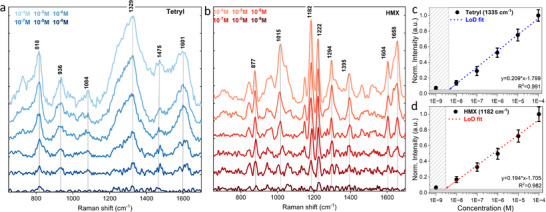
SERS data for Tetryl a) and HMX b) molecules accompanied with detection limit studies c,d) for 488 nm laser.
The vibrational properties of the cyclic HMX structure are in turn dominated by NO2 groups and CH2 groups in the cyclic structure. The peak at 877 cm−1 stands for the ring deformation or skeletal vibration modes in which CH2 groups are involved. The band at 1015 cm−1 is associated with symmetric N─NO2 stretching vibrations. The mode at 1182 and 1222 cm−1 is often associated with CH2 wagging or bending coupled with C─NO2 stretching vibrations. The peak at 1294 cm−1 represents NO2 symmetric stretching. The peak at 1395 cm−1 is due to CH2 bending or symmetrical NO2 stretching vibrations. The peak at 1604 cm−1 is associated with symmetric NO2 stretching and ring‐related vibrations. The mode at 1658 cm−1 is likely coupled C‐NO2 stretching.[ 44 , 45 , 46 , 47 ] The concentration behavior of two the most intense modes 1329 cm−1 for tetryl and 1182 cm−1 for HMX were monitored and their intensities plotted on a semilogarithmic scale (Figure 7c,d). After a linear fit (R2 > 0.980), it can be suggested that limit of detection is ≈4–5 nm for Tetryl and 2–3 nm for HMX molecule. Also, the HMX compound demonstrates slightly better RSD behavior at similar concentrations, which might be related to better stability of HMX in terms of volatilization under environmental conditions, thermal and photothermal stability.[ 48 , 49 ]
Finally, the same substrate was used to display the changes in the spectral profile of the molecular footprint upon different irradiation wavelengths commonly used in SERS (488, 535, and 633 nm). For example, in the case of silver nanostructures and nanoparticles for the same tetryl molecule, the position of the symmetrical NO2 stretching mode varies from 1357 to 1329 cm−1, depending on the laser used.[ 50 , 51 ] For this study, the substrate is first numerically verified, which shows a strong plasmonic coupling of the electric field for the selected lasers. Irregularities and structural imperfections of the plasmonic layer indicate that the shorter wavelengths efficiently activate smaller gaps, crevices, and particles. Lasers with longer wavelengths activate larger particles and gaps. Nevertheless, the maximum value of the field (V m−1) for the sample in the same XY plane (polarization along the x‐axis) remains in the same order of magnitude: 3.18 × 10⁷, 4.34 × 10⁷, and 2.56 × 10⁷ for 488, 535, and 633 nm, respectively (data extracted from Figure 8a–c). After measuring using similar laser powers settings, exposure times, and objectives the spectra of tetryl are displayed in Figure 8d. The figure suggests a noticeable redshift for the νsymNO2 from 1376 to 1327 cm−1 when considering 633 and 488 nm lasers. Also, modes are broader, similar to the situation reported by Milligan et al.[ 50 ]
Figure 8.

a–c) Electric field intensity distribution for the geometry mimicking the actual plasmonic layer deposited on the CuO surface for 633, 535, and 488 nm incident wavelengths; d) corresponding SERS spectra of the tetryl molecule with the same laser wavelength showing a broadening of the vibrational profile and a red shift of the electron‐accepting N═O bond of the tetryl.
The red shift is attributed to enhanced LUMO‐mediated CT (charge transfer), in which electrons are donated from the Fermi level of the Ag nanoparticle into the low‐lying LUMO of the nitro group of the tetryl. The increased electron density in the antibonding orbitals weakens the N═O bonds and shifts the vibrational frequency to lower wavenumbers. The broadening of Raman peaks in Ag‐tetryl SERS spectra is due to several contributing processes, including faster dephasing caused by stronger electron–vibrational coupling,[ 52 , 53 ] collateral thermal strain,[ 54 , 55 ] wavelength‐dependent plasmon resonances,[ 56 , 57 ] and chemical (charge‐transfer) enhancement.[ 58 ] In the following discussion, we navigate these effects but, importantly, neglect any CuO/Cu2O support because the oxide is completely shaded beneath an Ag layer thicker than the optical/electronic‐percolation threshold (< 10 nm) and can neither inject photocarriers nor tune the near field. Charge transfer (CT) itself reshapes the molecular polarizability: tetryls LUMO (≈–3.3 eV) and HOMO (≈–4.8 eV) flank the Ag‐Fermi level (≈–4.3 eV), leaving a 1.0 eV Ag → LUMO gap that dwarfs the 0.5 eV HOMO → Ag gap.[ 59 , 60 , 61 ] In Jensen's four‐orbital interaction representation,[ 56 , 57 ] the σ‐donation pathway is HOMOTetryl → Ag‐LUMO (in case of clusters < 2 nm, our case is Fermi level), while the chemically dominant π‐back‐bonding follows Ag‐Fermi → π*(NO2) LUMO, weakening the N─O bonds and red‐shifting νsym(NO2) from ≈1376 to ≈1327 cm−1. This adsorption‐induced charge leakage sets up a wavelength‐independent ground‐state dipole µGSCT that provides a constant, baseline chemical enhancement on top of which the photo‐induced dipole µPICT is modulated by the laser.[ 58 ]
At 488 nm (2.54 eV) and 535 nm (2.33 eV) the photons exceed the 1.0 eV gap by > 1.3 eV yet resonate with the blue‐shifted LSPR of sub‐20 nm particles and < 5 nm inter‐particle gaps. These hotspots i) provide intense ≈|E|4 fields that heat the lattice and lead to anharmonic broadening; ii) generate a dense, short‐lived flux of hot electrons that transiently occupy the π * orbital and contribute to lifetime broadening, although the average photoinduced dipole µPICT is only moderate (blue‐green photons sit well above the 0.96 eV Ag → LUMO gap, so only a small fraction of the hot‐electron continuum they generate is energy‐matched to the π(NO2) orbital, keeping the average µPICT below its resonant value even though the carrier flux is large); iii) exhibit steep field gradients that mix the fundamental with the combination bands, and iv) present a broad distribution of CT energies over countless sub‐5 nm nano‐gaps, leading to inhomogeneous broadening. Taken together, these mechanisms explain the particularly broad, red‐shifted NO2 bands recorded under blue–green excitation. The change to 633 nm (1.96 eV) and in theory to 785 nm (1.58 eV) reverses the balance. Larger particles and wider gaps lead to a redshift of the LSPR, so that both the photon energy and the plasmon converge on the 0.96 eV Ag → LUMO resonance; µPICT is now directly driven and reaches its maximum. At the same time, the hotspots are much weaker, thus the local heating decreases, the spread of CT energies decreases, leading to sharper and simultaneously CT‐improved spectra. Thus, the raw SERS signal is brightest at 488–535 nm, where the electromagnetic (EM) contribution dominates, while the red/NIR range provides the highest CT‐to‐EM ratio and the clearest view of the Ag → LUMO back‐donation, a balance that must be considered when compiling wavelength‐corrected vibrational datasets for machine‐learning classifiers that rely on accurate tracking of CT‐sensitive bonds commonly found in explosive molecules.
4. Conclusion
The presented structural defect‐rich plasmonic vertical 2D metasurface is synthesised in a one‐step oxygen plasma oxidation process where high‐energy oxygen ions bombard the copper surface, inducing local compressive stresses and generating abundant point defects that serve as nucleation centers for anisotropic CuO/Cu2O growth. Upon continuous plasma exposure (oxygen pressure 350 Pa, temperature 520 °C, time 20 min), the flux of reactive oxygen radicals and energetic ions significantly accelerates oxidation kinetics by lowering the activation barriers for both Cu→Cu2O and Cu2O→CuO transitions compared to classical thermal oxidation. Synergistically, these defect sites in conjunction with ion‐induced thermal stresses enhance the surface diffusion of copper atoms across the oxide interface, facilitating the coalescence of initial 1D CuO nanowires into extended 2D nanosheet arrays that align vertically on the substrate. The resulting 2D morphologies with the following average dimensions (width 5–10 µm, height 10–12 µm, thickness 1 µm at the roots and 50–100 nm at the ridges) were additionally decorated with Ag nanoparticles (10–50 nm in size) by magnetron sputtering. This transformed the structure into a highly active plasmonic sensor with an enhancement factor of 6 × 10⁶–9 × 10⁶, ensuring reliable nanomolar sensitivity for the highly explosive molecules tetryl and HMX in the dry SERS scenario with LoD 4–5 and 2–3 nm, respectively. Importantly, we are able to demonstrate the LUMO‐mediated charge‐transfer‐induced red‐shift of the symmetric NO2 stretching mode of tetryl for 633, 535, and 488 nm lasers, emphasizing the need for laser and substrate‐aware interpretation of vibration data for photosensitive hazardous compounds.
Conflict of Interest
The authors declare no conflict of interest.
Supporting information
Supporting Information
Acknowledgements
This research work on the development of high‐performance plasmonic 2D metastructures was financially supported by several national and international projects and programs. At first place, V.S. and D.V. are thankful to projects J2–50066 from the public agency for scientific research and innovation activity of the Republic of Slovenia (ARIS), NATO (Science for Peace and Security Program), NOOSE “Nanomaterials for Explosive Traces Detection with SERS” grant no. G5814. IJS's authors also acknowledge the ARIS program P1‐0417. JZ acknowledges the support from the European Innovation Council Pathfinder project under ThermoDust grant agreement No. 101046835. O.B. and A.B thank to a project awarded by the National Research Foundation of Ukraine, grant agreement no. 2020.02/0119. V.S. thanks to Dr. Evgeny Goreshnik for assistance with SERS measurement using the Horiba Jobin‐Yvon LabRAM HR spectrometer.
Shvalya V., Breus A., Baranov O., Vengust D., Zavašnik J., and Cvelbar U., “Plasma‐Tunable Metasurfaces for SERS Nanosensing of Hazardous Chemicals.” Small 21, no. 40 (2025): e06814. 10.1002/smll.202506814
Contributor Information
Vasyl Shvalya, Email: vasyl.shvalya@ijs.si.
Uroš Cvelbar, Email: uros.cvelbar@ijs.si.
Data Availability Statement
The data that support the findings of this study are available in the supplementary material of this article.
References
- 1. Shvalya V., Filipič G., Zavašnik J., Abdulhalim I., Cvelbar U., Appl. Phys. Rev. 2020, 7, 031307. [Google Scholar]
- 2. Sloan‐Dennison S., Wallace G. Q., Hassanain W. A., Laing S., Faulds K., Graham D., Nano Convergence 2024, 11, 33. [DOI] [PMC free article] [PubMed] [Google Scholar]
- 3. Kasani S., Curtin K., Wu N., Nanophotonics 2019, 8, 2065. [Google Scholar]
- 4. Byakodi M., Shrikrishna N. S., Sharma R., Bhansali S., Mishra Y., Kaushik A., Gandhi S., Biosens. Bioelectronics 2022, 12, 100284. [DOI] [PMC free article] [PubMed] [Google Scholar]
- 5. Chen M., Liu D., Du X., Lo K. H., Wang S., Zhou B., Pan H., TrAC, Trends Anal. Chem. 2020, 130, 115983. [Google Scholar]
- 6. Liu Y., Qin Z., Deng J., Zhou J., Jia X., Wang G., Luo F., Chemosensors 2022, 10, 455. [Google Scholar]
- 7. Liu Y., Kim M., Cho S. H., Jung Y. S., Nano Today 2021, 37, 101063. [Google Scholar]
- 8. Ruzi M., Celik N., Sahin F., Sakir M., Onses M. S., Small 2025, 21, 2408189. [DOI] [PMC free article] [PubMed] [Google Scholar]
- 9. Tian X., Zhang B., Song L., Bao J., Yang J., Sun L., Pei H., Song C., Battery Energy 2025, 4, e70023. [Google Scholar]
- 10. Mukherjee A., Wackenhut F., Dohare A., Horneber A., Lorenz A., Müchler H., Meixner A. J., Mayer H. A., Brecht M., J. Phys. Chem. C 2023, 127, 13689. [Google Scholar]
- 11. Wu J., Zhang L., Huang F., Ji X., Dai H., Wu W., J. Hazard. Mater. 2020, 387, 121714. [DOI] [PubMed] [Google Scholar]
- 12. Guselnikova O., Lim H., Kim H., Kim S. H., Gorbunova A., Eguchi M., Postnikov P., Nakanishi T., Asahi T., Na J., Yamauchi Y., Small 2022, 18, 2107182. [DOI] [PubMed] [Google Scholar]
- 13. Park S., Mun C., Xiao X., Braun A., Kim S., Giannini V., Maier S. A., Kim D., Adv. Funct. Mater. 2017, 27, 1703376. [Google Scholar]
- 14. Baranov O., Levchenko I., Bell J. M., Lim J. W. M., Huang S., Xu L., Wang B., Aussems D. U. B., Xu S., Bazaka K., Mater. Horiz. 2018, 5, 765. [Google Scholar]
- 15. Phan L., Yoon S., Moon M.‐W., Polymers 2017, 9, 417. [DOI] [PMC free article] [PubMed] [Google Scholar]
- 16. Bundaleska N., Tsyganov D., Dias A., Felizardo E., Henriques J., Dias F. M., Abrashev M., Kissovski J., Tatarova E., Phys. Chem. Chem. Phys. 2018, 20, 13810. [DOI] [PubMed] [Google Scholar]
- 17. Santhosh N. M., Shvalya V., Modic M., Hojnik N., Zavašnik J., Olenik J., Košiček M., Filipič G., Abdulhalim I., Cvelbar U., Small 2021, 17, 2103677. [DOI] [PubMed] [Google Scholar]
- 18. Guo B., Košiček M., Fu J., Qu Y., Lin G., Baranov O., Zavašnik J., Cheng Q., Ostrikov K., Cvelbar U., Nanomaterials 2019, 9, 1405. [DOI] [PMC free article] [PubMed] [Google Scholar]
- 19. Levchenko I., Xu S., Cherkun O., Baranov O., Bazaka K., Advances in Physics: X 2021, 6, 1834452. [Google Scholar]
- 20. Dey A., Ghosh P., Chandrabose G., Damptey L. A. O., Kuganathan N., Sainio S., Nordlund D., Selvaraj V., Chroneos A., St J Braithwaite N., Krishnamurthy S., Nano Select 2022, 3, 627. [Google Scholar]
- 21. Ding S.‐Y., Yi J., Li J.‐F., Ren B., Wu D.‐Y., Panneerselvam R., Tian Z.‐Q., Nat. Rev. Mater. 2016, 1, 16021. [Google Scholar]
- 22. Langer J., Jimenez De Aberasturi D., Aizpurua J., Alvarez‐Puebla R. A., Auguié B., Baumberg J. J., Bazan G. C., Bell S. E. J., Boisen A., Brolo A. G., Choo J., Cialla‐May D., Deckert V., Fabris L., Faulds K., García De Abajo F. J., Goodacre R., Graham D., Haes A. J., Haynes C. L., Huck C., Itoh T., Käll M., Kneipp J., Kotov N. A., Kuang H., Le Ru E. C., Lee H. K., Li J.‐F., Ling X. Y., et al., ACS Nano 2020, 14, 28. [DOI] [PMC free article] [PubMed] [Google Scholar]
- 23. Pérez‐Jiménez A. I., Lyu D., Lu Z., Liu G., Ren B., Chem. Sci. 2020, 11, 4563. [DOI] [PMC free article] [PubMed] [Google Scholar]
- 24. Kaur J., Khanna A., Kumar R., Chandra R., J. Mater. Sci.: Mater. Electron. 2022, 33, 16154. [Google Scholar]
- 25. Ha T., Park I., Sim K. I., Lee H., Bae J.‐S., Kim S. J., Kim J. P., Kim T.‐T., Kim J. H., Jang J. I., Jeong S.‐Y., APL Mater. 2019, 7, 031115. [Google Scholar]
- 26. Košiček M., Zavašnik J., Baranov O., Šetina Batič B., Cvelbar U., Cryst. Growth Des. 2022, 22, 6656. [Google Scholar]
- 27. Kochylas I., Gardelis S., Likodimos V., Giannakopoulos K., Falaras P., Nassiopoulou A., Nanomaterials 2021, 11, 1760. [DOI] [PMC free article] [PubMed] [Google Scholar]
- 28. Brimhall N., Herrick N., Allred D. D., Turley R. S., Ware M. J., Peatross J., Opt. Express 2009, 17, 23873. [DOI] [PubMed] [Google Scholar]
- 29. Kenmotsu S., Hirasawa M., Tamadate T., Matsumoto C., Osone S., Inomata Y., Seto T., ACS Omega 2024, 9, 37716. [DOI] [PMC free article] [PubMed] [Google Scholar]
- 30. Cañamares M. V., Chenal C., Birke R. L., Lombardi J. R., J. Phys. Chem. C 2008, 112, 20295. [Google Scholar]
- 31. Liu Y., Zhang Y., Tardivel M., Lequeux M., Chen X., Liu W., Huang J., Tian H., Liu Q., Huang G., Gillibert R., De La Chapelle M. L., Fu W., Plasmonics 2020, 15, 743. [Google Scholar]
- 32. Shi Y., Chen N., Su Y., Wang H., He Y., Nanoscale 2018, 10, 4010. [DOI] [PubMed] [Google Scholar]
- 33. Dimitriou A., Kastania A. S., Sarkiris P., Shvalya V., Papanikolaou N., Cvelbar U., Gogolides E., Micro Nano Engineer. 2024, 24, 100279. [Google Scholar]
- 34. Le Ru E. C., Blackie E., Meyer M., Etchegoin P. G., J. Phys. Chem. C 2007, 111, 13794. [Google Scholar]
- 35. Rodrigues D. C., De Souza M. L., Souza K. S., Dos Santos D. P., Andrade G. F. S., Temperini M. L. A., Phys. Chem. Chem. Phys. 2015, 17, 21294. [DOI] [PubMed] [Google Scholar]
- 36. Zhang W., Tian Q., Chen Z., Zhao C., Chai H., Wu Q., Li W., Chen X., Deng Y., Song Y., RSC Adv. 2020, 10, 23908. [DOI] [PMC free article] [PubMed] [Google Scholar]
- 37. Majumdar D., ACS Omega 2024, 9, 40242. [DOI] [PMC free article] [PubMed] [Google Scholar]
- 38. Qin X., Zhong B., Xu H., Jackman J. A., Xu K., Cho N.‐J., Lou Z., Wang L., Int. J. Extrem. Manuf. 2025, 7, 032003. [Google Scholar]
- 39. Guan R., Xu H., Lou Z., Zhao Z., Wang L., Appl. Phys. Rev. 2024, 11, 041327. [Google Scholar]
- 40. Ular N., Üzer A., Durmazel S., Erçağ E., Apak R., ACS Sens. 2018, 3, 2335. [DOI] [PubMed] [Google Scholar]
- 41. Banerjee D., Akkanaboina M., Kanaka R. K., Soma V. R., in Laser‐Based Micro‐ and Nanoprocessing XVII, (Eds: Kling R., Pfleging W., Watanabe A.), SPIE, San Francisco, United States: 2023, p. 19. [Google Scholar]
- 42. Vendamani V. S., Beeram R., Soma V. R., J. Alloys Compd. 2023, 959, 170573. [Google Scholar]
- 43. Akkanaboina M., Banerjee D., Kumar K. R., Goud R. S. P., Soma V. R., Rao S. V. S. N., Surfaces Interfaces 2023, 36, 102563. [Google Scholar]
- 44. Zhou M., Wei G., Zhang Y., Xiang D., Ye C., RSC Adv. 2022, 12, 32508. [DOI] [PMC free article] [PubMed] [Google Scholar]
- 45. Gao H., Wang Q., Ke X., Liu J., Hao G., Xiao L., Chen T., Jiang W., Liu Q., RSC Adv. 2017, 7, 46229. [Google Scholar]
- 46. Heleg‐Shabtai V., Zaltsman A., Sharon M., Sharabi H., Nir I., Marder D., Cohen G., Ron I., Pevzner A., RSC Adv. 2021, 11, 26029. [DOI] [PMC free article] [PubMed] [Google Scholar]
- 47. Ramachandran K., Kumari A., Acharyya J. N., Chaudhary A. K., Spectrochim. Acta, Part A 2021, 251, 119360. [DOI] [PubMed] [Google Scholar]
- 48. Sisco E., Najarro M., Samarov D., Lawrence J., Talanta 2017, 165, 10. [DOI] [PMC free article] [PubMed] [Google Scholar]
- 49. Pacheco‐Londoño L., Santiago A., Pujols J., Primera‐Pedrozo O. M., Mattei A., Ortiz W., Ruiz O., Ramirez M., Hernández‐Rivera S. P., (Eds: Andresen B. F., Fulop G. F., Norton P. R., Characterization of layers of Tetryl, TNB, and HMX on metal surfaces using fiber optics coupled grazing angle‐FTIR In Infrared Technology and Applications XXXIII), SPIE, Orlando, Florida, USA, 2007, Vol. 6542, pp. 1142–1151. [Google Scholar]
- 50. Milligan K., Shand N. C., Graham D., Faulds K., Anal. Chem. 2020, 92, 3253. [DOI] [PMC free article] [PubMed] [Google Scholar]
- 51. Banerjee D., Akkanaboina M., Kumar Kanaka R., Soma V. R., Appl. Surf. Sci. 2023, 616, 156561. [Google Scholar]
- 52. de Haas T., Smit R., Tebyani A., Bhattacharyya S., Watanabe K., Taniguchi T., Buda F., Orrit M., J. Phys. Chem. Lett. 2025, 16, 349. [DOI] [PMC free article] [PubMed] [Google Scholar]
- 53. Le Ru E. C., Etchegoin P. G., Principles of Surface‐Enhanced Raman Spectroscopy: And Related Plasmonic Effects, Elsevier, Amsterdam Boston, 2009. [Google Scholar]
- 54. Maher R. C., Cohen L. F., Le Ru E. C., Etchegoin P. G., Faraday Discuss. 2006, 132, 77. [DOI] [PubMed] [Google Scholar]
- 55. Le Ru E. C., Etchegoin P. G., Faraday Discuss. 2006, 132, 63. [DOI] [PubMed] [Google Scholar]
- 56. Jensen L., Aikens C. M., Schatz G. C., Chem. Soc. Rev. 2008, 37, 1061. [DOI] [PubMed] [Google Scholar]
- 57. Morton S. M., Jensen L., J. Am. Chem. Soc. 2009, 131, 4090. [DOI] [PubMed] [Google Scholar]
- 58. Cong S., Liu X., Jiang Y., Zhang W., Zhao Z., Innovation 2020, 1, 100051. [DOI] [PMC free article] [PubMed] [Google Scholar]
- 59. Puiu A., Giubileo G., Cesaro S. N., Bencivenni L., Appl. Spectrosc. 2015, 69, 1472. [DOI] [PubMed] [Google Scholar]
- 60. Tamuliene J., Sarlauskas J., Energies 2023, 16, 5180. [Google Scholar]
- 61. Sarvestani M. J., Ahmadi R., Chem. Methodol. 2020, 4, 40. [Google Scholar]
Associated Data
This section collects any data citations, data availability statements, or supplementary materials included in this article.
Supplementary Materials
Supporting Information
Data Availability Statement
The data that support the findings of this study are available in the supplementary material of this article.